Table of Contents
Advertisement
Quick Links
Introduction
The
B-G474E-DPOW1
Discovery kit is a digital power solution and a complete demonstration and development platform for the
®
STMicroelectronics Arm
Cortex
features, 96 Kbytes of embedded RAM, math accelerator functions, and USB PD3.0 offered by STM32G474RET6, the B-
G474E-DPOW1 Discovery kit helps the user to prototype applications with digital power such as a buck-boost converter, RGB
power LED lighting, or a class-D audio amplifier, based on the USB Type-C
Discovery kit does not require any separate probe as it integrates the STLINK-V3E debugger and programmer.
The STM32G474RET6 microcontroller features FMAC and CORDIC mathematical hardware accelerator, five 12-bits ADCs
(5 MSPS) up to 42 channels and with resolution up to 16-bit with hardware oversampling, seven 12-bit DAC channels, seven
ultra-fast rail-to-rail analog comparators, six operational amplifiers with PGA mode, seventeen timers with various advanced
2
functionalities, four I
C fast-mode plus, five USARTs, one LPUART, four SPIs, one SAI, three CAN‑FD controllers, one USB 2.0
full-speed interface and a UCPD block allowing connection to USB Type-C
random number generator, one FMC parallel synchronous interface, a quad-SPI memory interface, SWD and JTAG debugging
support.
This Discovery kit offers everything required for users to start and develop applications. The hardware features on the board
help to evaluate the following peripherals: USB Type-C
buck-boost application with Class-D audio amplifier and RGB power LED lighting. Thanks to its two 32-pin 2.54 mm pitch
extension connectors, it also enables users to plug it on a breadboard for prototyping. The integrated STLINK-V3E provides an
embedded in-circuit debugger and programmer for the STM32 MCU.
The B-G474E-DPOW1 Discovery kit comes with the STM32 comprehensive free software libraries and examples available with
the STM32Cube package.
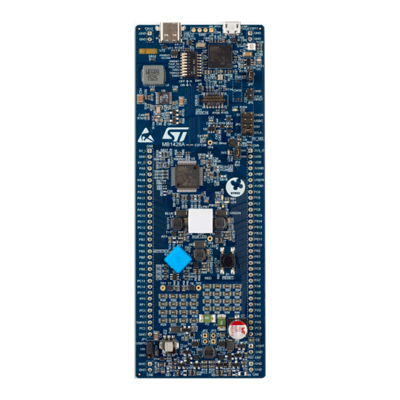
Figure 1.
B-G474E-DPOW1 top view
Pictures are not contractual.
UM2577 - Rev 2 - September 2020
For further information contact your local STMicroelectronics sales office.
®
-M4 core-based STM32G474RET6 microcontroller. Leveraging the new HRTimer-oriented
®
compatible with USB PD3.0, HRTimer evaluation, digital power for
Discovery kit with STM32G474RE MCU
®
2.0 FS connector interface. The B-G474E-DPOW1
®
compatible with USB Power Delivery, a true
Figure 2.
B-G474E-DPOW1 bottom view
UM2577
User manual
www.st.com
Advertisement
Table of Contents

Related Manuals for STMicroelectronics B-G474E-DPOW1


Summary of Contents for STMicroelectronics B-G474E-DPOW1
-
Page 1: Figure 1. B-G474E-Dpow1 Top View
The integrated STLINK-V3E provides an embedded in-circuit debugger and programmer for the STM32 MCU. The B-G474E-DPOW1 Discovery kit comes with the STM32 comprehensive free software libraries and examples available with the STM32Cube package. -
Page 2: Features
UM2577 Features Features ® ® • STM32G474RET6 Arm Cortex -M4 core-based microcontroller, featuring 512 Kbytes of Flash memory and 128 Kbytes of SRAM, in LQFP64 package ® • USB Type-C with USB 2.0 FS interface compatible with USB-PD 3.0 • RGB power LED for a bright lighting •... -
Page 3: Ordering Information
UM2577 Ordering information Ordering information To order the B-G474E-DPOW1 Discovery kit, refer to Table 1. Additional information is available from the datasheet and reference manual of the target STM32. Table 1. Ordering information Order code Board reference Target STM32 B-G474E-DPOW1... -
Page 4: Development Environment
IAR Systems - IAR Embedded Workbench ® • Keil - MDK-ARM • STMicroelectronics - STM32CubeIDE 1. On Windows ® only. Demonstration software The demonstration software, included in the STM32Cube MCU Package corresponding to the on-board microcontroller, is preloaded in the STM32 Flash memory for easy demonstration of the device peripherals in standalone mode. -
Page 5: Technology Partners
UM2577 Technology partners Technology partners • Wurth Electronics: – Current sense transformer, 1:125 ratio, 6 to 6.5 mΩ, 3 mH, 10 A, part number 749251125 UM2577 - Rev 2 page 5/54... -
Page 6: Conventions
UM2577 Conventions Conventions Table 2 provides the conventions used for the ON and OFF settings in the present document. Table 2. ON/OFF convention Convention Definition Jumper JPx ON Jumper fitted Jumper JPx OFF Jumper not fitted Jumper JPx [1-2] Jumper fitted between Pin 1 and Pin 2 Solder bridge SBx ON SBx connections closed by 0 Ω... -
Page 7: Limitations
UM2577 Limitations Limitations ® USB Type-C limitation ® By default, only a USB Type-C nominal voltage of 5 V must be used. For any other V nominal voltage, refer to the technical application note and specific configuration. Debug connector configuration According to the board revision, an STDC14 or a MIPI10 connector is soldered onto the CN1 STDC14 footprint. -
Page 8: Quick Start
User LEDs LD2, LD3, LD4, and LD5 scroll, indicating the demonstration application software startup. The demo application software and its user manual, as well as other software examples for exploring STM32G4 features are available at B-G474E-DPOW1. Develop an application using the available examples. -
Page 9: Hardware Layout And Configuration
UM2577 Hardware layout and configuration Hardware layout and configuration The B-G474E-DPOW1 Discovery kit is designed around the STM32G474RET6 microcontroller, in 64-pin LQFP package. The hardware block diagram (Refer to Figure 3) illustrates the connection between the microcontroller and the peripherals (RGB power LED and buck LED, digital power buck-boost, LTC3114 5 V converter, ®... -
Page 10: Figure 3. Hardware Layout And Configuration
UM2577 Hardware layout and configuration Figure 3. Hardware layout and configuration USB 2.0 FS Micro-USB Type- ® receptacle Embedded 3.3V power TAG connector VREF STLINK-V3E POWER DEBUG Joystick Octal connector RESET 4-direction mechanical oscillator button + Center key switch SWD / UCPD I/Os NRST... -
Page 11: Product Layout (Top And Bottom)
UM2577 Product layout (top and bottom) Product layout (top and bottom) Figure 4. B-G474E-DPOW1 top layout view USB micro-B Type-C ® ST-LINK receptacle receptacle LD9 COM LED Octal mechanical LD8 overcurrent LED switch U9 STLINK-V3E MCU JP7 TNRST U6 LTC3114-1... -
Page 12: Figure 5. B-G474E-Dpow1 Bottom Layout View
UM2577 Product layout (top and bottom) Figure 5. B-G474E-DPOW1 bottom layout view CN11 CN12 Corner jumper Corner jumper CN10 TAG connector 32-pin extension 32-pin extension connector connector VOUT extension connector CN11 Corner jumper Corner jumper UM2577 - Rev 2 page 12/54... -
Page 13: Mechanical Drawing
UM2577 Mechanical drawing Mechanical drawing Figure 6. B-G474E-DPOW1 mechanical drawing 55.88 mm 6.35 mm 6.35 mm 1.5 mm 6.35 mm UM2577 - Rev 2 page 13/54... -
Page 14: Embedded Stlink-V3E
5V_SELECTION measurement The B-G474E-DPOW1 product can be powered from the CN3 ST-LINK USB connector (STLK), but the host PC only provides 100 mA to the ST-LINK circuit until the end of USB enumeration. Then, the B-G474E-DPOW1 product asks for the 500 mA power to the host PC. -
Page 15: Deactivation
OFF and the 5 V power reference of the board is OFF. The 5 V Green LED LD7 is turned OFF. The Green LED LD7 is turned ON when the B-G474E-DPOW1 product is powered by the 5V correctly. The COM LED LD9 indicates the STLINK-V3E communication status with the host, refer to Overview of ST-LINK derivatives technical note (TN1235). -
Page 16: Stlink-V3E Drivers
UM2577 STLINK-V3E drivers Figure 9. SW1 and JP7 TNRST default configurations Table 4. SW1 configuration Pin number Function STLINK-V3E description State Comment Connect or isolate STLINK-V3E from PWREXT T_PWR_EXT (PB1) ON or OFF general 5V power presence indicator Connect or isolate STLINK-V3E from VCCAIN T_VCC_AIN (PA0) ON or OFF... -
Page 17: Stlink-V3E Vcp Configuration
UM2577 STLINK-V3E VCP configuration Figure 10. USB composite device STLINK-V3E VCP configuration STLINK-V3E supports Virtual COM port (VCP) by default. To disable this function, the relevant SW1 switches linked to the VCP function can be set to the OFF state (See Table 4. -
Page 18: Power Supply
The following diagram describes the power architecture and the maximum voltage and current limits, under which functions can be safely used on the B-G474E-DPOW1 product. In any case, ensure the total power budget of the application always conforms to the selected 5V power source mode, if not malfunction can occur. For detailed configuration, refer to the relevant function description and technical application notes. -
Page 19: Figure 11. Power Diagram
Figure 11. Power diagram POWER DIAGRAM SB38 ON 5V_OUT 3V3_OUT => Up to 500 mA 5V_OUT BUCKS Type-C + RGB ® STLINK R133 => Up to 250 mA V_LED POWER 30 mA USER LEDs / USBPD_VBUS 5V_USB_CHGR JOYSTICK => 5V to 15 V 5V nominal voltage nominal voltage =>... -
Page 20: Power Source Selection
10.2 Power source selection The B-G474E-DPOW1 product is designed to be powered by a 5 V DC power supply. It is possible to configure the Discovery board with JP5 header to use any of the four sources described in Table 6 for the 5 V DC power supply. -
Page 21: Chgr
100 mA current limit before enumeration, which is not sufficient to start the product. • Any other USB Host can supply and startup the B-G474E-DPOW1 board, like a dumb USB wall charger or a ® USB battery charging 1.2 Host or a USB Type-C Host. -
Page 22: Microcontroller Power
UM2577 Microcontroller power Figure 15. JP5 (E5V) from CN9 (5V_I / GND) 10.3 Microcontroller power By default, the STM32G474RET6 microcontroller power supplies are all connected to the VDD power supply. In case the user wants to test any other power supply configuration, few solder bridges can be modified (Refer to Section 15.2 VDD power supply is connected in the design to 3V3, 3.3 V-regulated output, which can draw a current up to 500 mA. -
Page 23: Clock Sources
UM2577 Clock sources Clock sources The B-G474E-DPOW1 Discovery kit is using the internal HSI clock reference. In case the user wants to apply external clock sources, there are three possible options: • X2, 24MHz oscillator footprint (not fitted by default) •... -
Page 24: Boot Options
Boot options Boot options By default, the B-G474E-DPOW1 boots on the STM32G474RET6 internal Flash, thanks to the nSWBOOT0 option bit set to zero. Thus, by default, the Boot procedure is completely managed by software. But, as the PB8 pin of the STM32G474RET6 is also free for use by default, the user can choose any boot... -
Page 25: Board Functions
Rev 1.3, USB PD3.0, and with USB battery charging 1.2. Caution: ® The B-G474E-DPOW1 Discovery kit does not support the connection of low-power USB Hosts on USB Type-C ® CN2 connector. As required by the USB Type-C specification, the B-G474E-DPOW1 product can interface on CN2 with USB2.0 and USB3.x Legacy High power Hosts supporting USB Full speed data link, but some feature... -
Page 26: Power Input To The Digital Power Buck-Boost Feature
Power input to the digital power buck‑boost feature ® The USB Type-C CN2 connector can also be used as a power input to demonstrate the digital power buck‑boost converter feature of the B-G474E-DPOW1 product (Refer to Section 13.2 Digital power buck- boost converter):... -
Page 27: Power And Data Input To The Audio Class-D Amplifier Feature
BUCKBOOST_I_IN_AVG (PA2) for ADC conversion. 13.2 Digital power buck-boost converter The B-G474E-DPOW1 includes a digital power buck-boost converter feature with two embedded resistor load networks on VOUT. Attention: The digital power buck-boost converter feature may not support the JP5 setting on USBC. Refer to dedicated application note for additional specific conditions. -
Page 28: Figure 17. Digital Power Buck-Boost Converter
UM2577 Digital power buck-boost converter Figure 17. Digital power buck-boost converter Embedded VOUT resistor loads JP2 / JP3 headers CN7 (top) VIN selection VOUT / GND The buck-boost converter function is composed of symmetrical half-bridge topology and works in either Buck, Boost, or Buck-boost mode. -
Page 29: Audio Class-D Amplifier
RGB power LED Attention: According to the photobiological safety of lamps and lamp systems (IEC62471), the B-G474E-DPOW1 product is rated Risk 1 in its default configuration (low risk). The most restrictive optical radiation is the retinal blue light hazard 300 to 400 nm. Associated technical reports with exposure hazard values and exposure distance are deliverable on demand. -
Page 30: Extension Connector Headers
Section 14.5 CN8 extension connector). Caution: When the B-G474E-DPOW1 Discovery board is used in standalone, take care to put it on a non-conductive material to avoid short circuits on all bottom side connectors or permanent damage can occur. UM2577 - Rev 2... -
Page 31: Figure 20. Cn8 And Cn9 Extension Connectors
Connector spacing is (17 x 2.54) 43.18 mm. They offer easy access to signal pins on the bottom and top sides of the Discovery Board. Thus, the B-G474E-DPOW1 product is compatible with standard breadboards for prototyping. To allow a complete board connection, the CN5, CN6, CN11, CN12 GND corner headers, and the CN7 VOUT/GND connector are also compatible with the 2.54 mm pitch grid. -
Page 32: Rc Sinus Function
During reset activation, the LD2 blue user LED is lit in low luminance. PA15 has an internal pull-up during reset and it drives this LD2 with low current. 13.9 Buttons and LEDs function Table 12 summarizes the different buttons and LEDs of the B-G474E-DPOW1 Discovery kit and their function: Table 12. Buttons and LEDs Reference Color... -
Page 33: Connectors
UM2577 Connectors Connectors Eleven connectors are implemented on the B-G474E-DPOW1 product: • CN3: USB Micro-B ® • CN2: USB Type-C • CN1: Debug connector • CN10: TAG connector • CN8: Extension connector header • CN9: Extension connector header • CN7: VOUT connector header •... -
Page 34: Cn1 Debug Connector
UM2577 CN1 debug connector Description Signal assignment Description Signal assignment number number TX2_N RX2_N TX2_P RX2_P 14.2 CN1 debug connector Different debug connectors are used according to Discovery board revisions : • An STDC14 14-pin connector is soldered on CN1 for BG474EDPOW1$AT1 finish good (Based on MB1428- G474RE-B01 board revision) •... -
Page 35: Cn1 Mipi10 Debug Connector
UM2577 CN1 debug connector Description Assignment Description Assignment number number T_VCP_RX (PC11) T_VCP_TX (PC10) Note: 4-wire and 5-wire JTAG Debug modes are not supported by default. 4-wire JTAG mode may be used, but may ® require to deactivate USB Type-C feature in hardware and software, to connect JTDI with the SB28 solder bridge and to disconnect R89. -
Page 36: Cn10 Tag Connector
14.4 CN9 extension connector The 32-pin CN9 extension connector is accessible on the left-hand-side on top of the B-G474E-DPOW1, or on the right-hand-side of its bottom. It provides access to some PIOs of STM32G474RET6 and most of the Discovery board power supplies. It can be plugged on a breadboard for prototyping (2.54 mm pitch). All pins remain accessible on the top side for probing. -
Page 37: Cn8 Extension Connector
14.5 CN8 extension connector The 32-pin CN8 extension connector is accessible on the right-hand-side on top of the B-G474E-DPOW1, or on the left-hand side of its bottom. It provides access to some PIOs of STM32G474RET6 and some Discovery board power supplies. It can be plugged on a breadboard for prototyping (2.54 mm pitch). All pins remain accessible on the top side for probing. -
Page 38: Table 18. Cn8 Extension Connector
UM2577 CN8 extension connector Table 18. CN8 extension connector Description Main function Signal assignment Optional modification number 3V3_O Power 3V3_OUT Power Power AGND Power AGND VREF Power VREF VREFP Power VREFP AVDD Power AVDD PC9 (Free) RGB LED BUCK_GREEN_DRIVE Remove R72 RC sinus RC sinus function Remove R97... -
Page 39: Cn7 Vout Extension Connector
CN7 VOUT extension connector The CN7 extension connector is accessible on the right-hand-side on top of the B-G474E-DPOW1, or on the left- hand-side of its bottom. It provides access to VOUT, buck-boost output voltage, and GND. It can be plugged on a breadboard for prototyping (2.54 mm pitch). -
Page 40: Jumpers And Solder Bridges
UM2577 Jumpers and solder bridges Jumpers and solder bridges 15.1 Jumpers The jumper functions and their default status are described in Table 21 Table 21. Jumper configuration Reference Jumper Function Comment Connect buck‑boost VIN to the V from USB Type- [1-2] VIN connected to USBPD ®... -
Page 41: Solder Bridges
UM2577 Solder bridges 15.2 Solder bridges The jumper functions and their default status are described in Table Table 22. Solder bridges configuration SB name Status Function Comment AGND to GND connection near digital Connect AGND to GND plan near T3 power buck-boost for analog Isolate AGND from GND plan near T3 measurements... - Page 42 UM2577 Solder bridges SB name Function Comment Status Connect PB3 to T_SWO SB16 PB3 connection to T_SWO Isolate PB3 from T_SWO, PB3 can be used for any other applications at the CN9 extension connector. Connect VREF+ / VREFP to VDDA / AVDD VREF+ / VREFP connection to VDDA / SB17 AVDD...
- Page 43 UM2577 Solder bridges SB name Function Comment Status Power 3V3_STLK from 5V_USBPD when USB Type- ® is plugged SB31 Power 3V3_STLK from 5V_USBPD No power on 3V3_STLK from 5V_USBPD when USB ® Type-C is plugged Automatic Burst/PWM Mode is activated LTC3114-1 Automatic Burst /PWM Mode SB32 control...
-
Page 44: Stm32G474Ret6 Gpio And Pin Assignment
UM2577 STM32G474RET6 GPIO and pin assignment STM32G474RET6 GPIO and pin assignment Table 23. STM32G474RET6 GPIO and pin assignment Extension connector Pin number Pin name Signal assignment Main function number VBAT MCU power PC13 JOYSTICK_SELECT Joystick PC14-OSC32_IN BUCKBOOST_LOAD_50% Buck-boost PC15- BUCKBOOST_LOAD_100% Buck-boost OSC32_OUT PF0-OSC_IN... - Page 45 UM2577 STM32G474RET6 GPIO and pin assignment Extension connector Pin number Pin name Signal assignment Main function number PB13 BUCKBOOST_N1_DRIVE Buck-boost PB14 BUCKBOOST_N2_DRIVE Buck-boost PB15 BUCKBOOST_P2_DRIVE Buck-boost BUCK_RED_DRIVE RGB LED RC sinus function RC sinus BUCK_GREEN_DRIVE RGB LED PC9 (Free) BUCK_BLUE_DRIVE RGB LED USBPD_DBCC1 USBPD...
-
Page 46: Appendix A Federal Communications Commission (Fcc) And Ised Canada Compliance
(2) this device must accept any interference received, including interference that may cause undesired operation. Part 15.21 Any changes or modifications to this equipment not expressly approved by STMicroelectronics may cause harmful interference and void the user's authority to operate this equipment. Part 15.105 This equipment has been tested and found to comply with the limits for a Class B digital device, pursuant to part 15 of the FCC Rules. - Page 47 UM2577 ISED Compliance Statement Étiquette de conformité à la NMB-003 d'ISDE Canada : CAN ICES-3 (B) / NMB-3 (B). UM2577 - Rev 2 page 47/54...
-
Page 48: Revision History
UM2577 Revision history Table 24. Document revision history Date Revision Changes 12-Jul-2019 Initial release. Added: • Section 6.2 Debug connector configuration Updated: 8-Sep-2020 • Section 14.2 CN1 debug connector split in STDC14 and MIPI10 sections • Section Appendix A Federal Communications Commission (FCC) and ISED Canada Compliance Statements Class B compliancy UM2577 - Rev 2... -
Page 49: Table Of Contents
UM2577 Contents Contents Features................2 Ordering information . - Page 50 UM2577 Contents Clock sources ..............23 Boot options .
- Page 51 UM2577 Contents FCC Compliance Statement ........... . 46 ISED Compliance Statement .
-
Page 52: List Of Tables
UM2577 List of tables List of tables Table 1. Ordering information..............3 Table 2. -
Page 53: List Of Figures
B-G474E-DPOW1 mechanical drawing ........ - Page 54 IMPORTANT NOTICE – PLEASE READ CAREFULLY STMicroelectronics NV and its subsidiaries (“ST”) reserve the right to make changes, corrections, enhancements, modifications, and improvements to ST products and/or to this document at any time without notice. Purchasers should obtain the latest relevant information on ST products before placing orders. ST products are sold pursuant to ST’s terms and conditions of sale in place at the time of order acknowledgement.
Need help?
Do you have a question about the B-G474E-DPOW1 and is the answer not in the manual?
Questions and answers