ON Semiconductor RSL10 Manual
Evaluation and development board
Hide thumbs
Also See for RSL10:
- Hardware reference manual (521 pages) ,
- Getting started (51 pages) ,
- User manual (21 pages)

Subscribe to Our Youtube Channel
Related Manuals for ON Semiconductor RSL10


Summary of Contents for ON Semiconductor RSL10
- Page 1 RSL10 Evaluation and Development Board Manual M-20835-005 August 2017 © SCILLC, 2017 Previous Edition © 2017 “All Rights Reserved”...
- Page 2 PUBLICATION ORDERING INFORMATION LITERATURE FULFILLMENT: N. American Technical Support: 800-282-9855 Toll ON Semiconductor Website: www.onsemi.com Literature Distribution Center for ON Semiconductor Free USA/Canada P.O. Box 5163, Denver, Colorado 80217 USA Europe, Middle East and Africa Technical Support: Order Literature: http://www.onsemi.com/orderlit...
-
Page 3: Table Of Contents
ON Semiconductor Table of Contents Page 1. Introduction ....... . 4 1.1 Purpose . -
Page 4: Introduction
1.1 P URPOSE This manual provides detailed information about the configuration and use of the RSL10 Evaluation and Development Board, both the wafer level chip scale package (WLCSP) and the quad flat no-leads (QFN) package. The Evaluation and Development Board is designed to be used with the software development tools to evaluate the performance and capabilities of the RSL10 radio System-on-Chip (SoC). -
Page 5: Further Reading
Appendix F: QFN Bill of Materials contains a list of the parts that are used to manufacture the QFN Evaluation and Development Board. 1.5 F URTHER EADING For more information, refer to the following documents: • RSL10 Software Development Tools User’s Guide • Firmware Reference Manual for RSL10 • Hardware Reference Manual for RSL10 • RSL10 Datasheet... -
Page 6: Overview
RSL10 SWJ-DP debug port signals to the USB of the host PC. There is also an on-board 4-bit level shifter for debugging; it translates the I/O signal level of RSL10 to the 3.3 V digital logic level. It is not enabled by default;... -
Page 7: Evaluation And Development Board
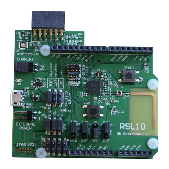
OARD ESIGN The following sections detail the various sub-circuits of the RSL10 Evaluation and Development Board. The block diagram in Figure 3 shows the locations of the various circuit sections for the WLCSP board. The block diagrams in Figure 4 and Figure 5 show the locations of the circuit sections for the QFN board. Figure 6 and Figure 7 provide 3-dimensional illustrations of the QFN board. - Page 8 Evaluation and Development Board Manual Figure 3. Circuit Location Block Diagram for WLCSP Board www.onsemi.com...
- Page 9 ON Semiconductor Figure 4. Circuit Location Block Diagram for QFN Board (Top View) www.onsemi.com...
- Page 10 Evaluation and Development Board Manual Figure 5. Circuit Location Block Diagram for QFN Board (Bottom View) www.onsemi.com...
- Page 11 ON Semiconductor Figure 6. Three-Dimensional Line Drawing of the QFN Board (Top View) www.onsemi.com...
-
Page 12: Power Supply
Evaluation and Development Board Manual Figure 7. Three-Dimensional Line Drawing of the QFN Board (Bottom View) 3.3 P OWER UPPLY The Evaluation and Development Board can be powered by one of the following: • Micro USB port with regulator • External power supply connector (P5 for QFN, P9 for WLCSP) with regulator •... -
Page 13: Level Translators
EVEL RANSLATORS The board has level translators for the DIO signals of RSL10, including the clock signal. The level translators facilitate interfacing to external devices that operate at a higher voltage than RSL10. VDDO and 3.3 V are two different power rails. The translator allows a logic signal on the VDDO side to be translated to either a higher or a lower logic signal voltage on the 3.3 V side, and vice-versa. -
Page 14: Led Circuitry
There are two LEDs on the board. One is a dual color LED, called LD1, connected to the J-Link emulator microcontroller unit (MCU). The other is the green LED, connected to DIO 6 of RSL10. You can use this LED within your applications as an indication LED by programming DIO 6. -
Page 15: Digital Input/Output (Dio)
NPUT UTPUT RSL10 contains 16 digital I/O (DIO) signals. The DIO voltage domain is VDDO, while the input voltage can be VBAT or external voltage as outlined in Section 3.6, “Measuring the Current Consumption” on page 14. The DIO signals on RSL10 are multiplexed with several interfaces, including: •... -
Page 16: 3.9.2 Qfn Power Supplies
Evaluation and Development Board Manual • VDDRF • 3.9.2 QFN Power Supplies The external power supplies available for QFN boards are: • VBUS, 5 V from USB connection — available only when USB is plugged in • V3.3, 3.3 V from LDO — available when regulated supply is selected •... -
Page 17: Wlcsp Connectors
External power supply header Input and output of level shifter Power supply on board and supply voltage configuration header A.4 S WITCHES Table 6. Switch Descriptions Designator Description RESET Pushbutton switch to reset RSL10 DIO5 Pushbutton switch for DIO5 www.onsemi.com... -
Page 18: Connectors
Evaluation and Development Board Manual A.5 C ONNECTORS Table 7. Connector Descriptions Designator Description Micro USB port for power supply, JTAG and UART emulation www.onsemi.com... -
Page 19: Qfn Connectors
Arduino IOH header I2C, SPI1 External JTAG debug connection header Current measurement header External power supply header Input and output of level shifter B.4 S WITCHES Table 10. Switch Descriptions Designator Description Pushbutton switch to reset RSL10 Pushbutton switch for DIO5 www.onsemi.com... -
Page 20: Connectors
Evaluation and Development Board Manual B.5 C ONNECTORS Table 11. Connector Descriptions Designator Description RF switch connector Micro USB port for power supply, JTAG and UART emulation MCU programming connector Digilent PMOD peripheral connector I2C, SPI1, INT0 Battery Holder (12mm coin cell) www.onsemi.com... -
Page 21: Wlcsp Schematics
WLCSP Schematics This appendix contains schematics for the WLCSP Evaluation and Development Board: • The interface MCU schematic • The RSL10 schematic • The power supply schematic These schematics are for Version 1.1 and Version 1.2 of the WLCSP board. www.onsemi.com... - Page 22 Evaluation and Development Board Manual Shield TRSTin PA0/TIOB0/NPCS1 CTS0/A1/AD3/PB8 TRSTout PA1/TIOA0/NPCS2 RTS0/A0/NBS0/AD2/PB7 PA2/TCLK0/AD12BTRG TIOB1/D15/AD1/PB6 TRESin PA3/MCCK/PCK1 TIOA1/A7/AD0/PB5 TRESout PA4/MCCDA/PWMH0 RD/PCK0/PA27 PA5/MCDA0/PWMH1 D4/PWMH0/PB13 PA6/MCDA1/PWMH2 D3/RI0/PB12 PA7/MCDA2/PWML0 D2/DCD0/PB11 VDDCORE PWMH2/A4/PB2 PWMH1/A3/PB1 VDDIO PWMH0/A2/PB0 PA8/MCDA3/PWML1 PA9/TWD0/PWML2 VDDIO PA10/TWCK0/PWML3 VDDCORE PA11/URXD/PWMFI0 RF/TIOB2/PA31 PA12/UTXD/PWMFI1 RK/PWMH1/PA29 FWUP TK/PWMH0/PA28 ERASE...
- Page 23 ON Semiconductor WAKEUP NRESET NRESET EN_TEST VBAT1 VSSC VBAT VSSA VDDPA VSSPA VDDC VSSRF VDDM XBO5 VDDSYN_SW VSSL VDDRF_SW XBO2 VDDRF DIO0 VDDA DIO1 VDDO DIO2 JTCK DIO3 JTMS TRST TRST Figure 9. RSL10 Schematic www.onsemi.com...
- Page 24 Evaluation and Development Board Manual WAKEUP Figure 10. Power Supply Schematic www.onsemi.com...
-
Page 25: Qfn Schematics
APPENDIX D QFN Schematics This appendix contains schematics for the QFN Evaluation and Development Board, version 1.3: • The top-level (Arduino interface) schematic • The RSL10 schematic • The Interface MCU schematic • The power supply schematic www.onsemi.com... - Page 26 Evaluation and Development Board Manual TDOin TDOin TDOin TDIin TDIin TDIin TRSTin TRSTin TRSTin TMSin JTAG_TMS TMSin JTAG_TMS TCKin JTAG_TCK TCKin JTAG_TCK TRESin TRESin RESET Figure 11. Top-Level (Arduino Interface) Schematic www.onsemi.com...
- Page 27 ON Semiconductor VBAT VDDPA VSSPA VDDC VSSA VSSD VDDM VSSD VDDSYN_SW VDDRF_SW VSSRF VDDRF VDDA VDDO Figure 12. RSL10 SoC Schematic www.onsemi.com...
- Page 28 Evaluation and Development Board Manual Shield TRSTin PA0/TIOB0/NPCS1 CTS0/A1/AD3/PB8 TRSTout PA1/TIOA0/NPCS2 RTS0/A0/NBS0/AD2/PB7 PA2/TCLK0/AD12BTRG TIOB1/D15/AD1/PB6 TRESin PA3/MCCK/PCK1 TIOA1/A7/AD0/PB5 TRESout PA4/MCCDA/PWMH0 RD/PCK0/PA27 PA5/MCDA0/PWMH1 D4/PWMH0/PB13 PA6/MCDA1/PWMH2 D3/RI0/PB12 PA7/MCDA2/PWML0 D2/DCD0/PB11 VDDCORE PWMH2/A4/PB2 PWMH1/A3/PB1 VDDIO PWMH0/A2/PB0 PA8/MCDA3/PWML1 PA9/TWD0/PWML2 VDDIO PA10/TWCK0/PWML3 VDDCORE PA11/URXD/PWMFI0 RF/TIOB2/PA31 PA12/UTXD/PWMFI1 RK/PWMH1/PA29 FWUP TK/PWMH0/PA28 ERASE...
- Page 29 ON Semiconductor Figure 14. Power Supply Schematic www.onsemi.com...
-
Page 30: Wlcsp Bill Of Materials
APPENDIX E WLCSP Bill of Materials This appendix lists the parts that were used to make the WLCSP Evaluation and Development Board. Table 12. Bill of Materials for RSL10 WLCSP Evaluation and Development Board Version 1.2 Manufacturer Part Designator Description... - Page 31 ON Semiconductor Table 12. Bill of Materials for RSL10 WLCSP Evaluation and Development Board Version 1.2 (Continued) Manufacturer Part Designator Description Footprint Doc Supplier part number Number CONN HEADER 4POS HDR_2x2 1241050-2 A121785CT-ND BRKWAY DL GOLD CONN HEADER 3POS HDR_3x1’...
- Page 32 Evaluation and Development Board Manual Table 12. Bill of Materials for RSL10 WLCSP Evaluation and Development Board Version 1.2 (Continued) Manufacturer Part Designator Description Footprint Doc Supplier part number Number See installation next CONN JUMPER SPC02SYAN S9001-ND page (2.54mm) Gold...
-
Page 33: Qfn Bill Of Materials
APPENDIX F QFN Bill of Materials This appendix lists the parts that were used to make the QFN Evaluation and Development Board. Table 13. Bill of Materials for RSL10 QFN Evaluation and Development Board Version 1.3 Manufacturer Part Designator Description... - Page 34 Evaluation and Development Board Manual Table 13. Bill of Materials for RSL10 QFN Evaluation and Development Board Version 1.3 (Continued) Manufacturer Part Designator Description Footprint Doc Supplier part number Number WR-PHD 2.54 mm 613012243121 S5559-ND Angled Dual Socket Header, 12p...
- Page 35 ON Semiconductor Table 13. Bill of Materials for RSL10 QFN Evaluation and Development Board Version 1.3 (Continued) Manufacturer Part Designator Description Footprint Doc Supplier part number Number R3, R5, R6, R26, Resistor, ±1%, 0402 ERJ-2RKF68R0X, P68.0LCT-ND, P68.0LCT-ND, R27, R32,R44, R46, 0.063W...
- Page 36 Evaluation and Development Board Manual Table 13. Bill of Materials for RSL10 QFN Evaluation and Development Board Version 1.3 (Continued) Manufacturer Part Designator Description Footprint Doc Supplier part number Number See Jumper CONN JUMPER CONN JUMPER (2.54mm) SPC02SYAN S9001-ND Location...
- Page 37 PUBLICATION ORDERING INFORMATION LITERATURE FULFILLMENT: N. American Technical Support: 800-282-9855 Toll ON Semiconductor Website: www.onsemi.com Literature Distribution Center for ON Semiconductor Free USA/Canada P.O. Box 5163, Denver, Colorado 80217 USA Europe, Middle East and Africa Technical Support: Order Literature: http://www.onsemi.com/orderlit...
Need help?
Do you have a question about the RSL10 and is the answer not in the manual?
Questions and answers