Advertisement
Quick Links
EVBUM2565/D
RSL10 SIP Evaluation and
Development Board
User's Manual
INTRODUCTION
Purpose
This manual provides detailed information about the
configuration and use of the RSL10 SIP Evaluation and
Development
Evaluation and Development Board is designed to be used
with the software development tools to evaluate the
performance and capabilities of the RSL10 SIP radio.
Manual Organization
The Evaluation and Development Board Manual contains
the following chapters and appendices:
•
Chapter 1: Introduction describes the purpose of this
manual, describes the target reader, explains how the
book is organized, and provides a list of suggested
reading for more information.
•
Chapter 2: Overview provides an overview of the
Evaluation and Development Board described in this
manual.
•
Chapter 3: Evaluation and Development Board
provides the details of the Evaluation and Development
Board. The chapter is divided into the following topics:
Development Board Setup
♦
Development Board Design
♦
Power Supply
♦
Level Translators
♦
LED Circuitry
♦
RSL10 SIP
♦
Measuring the Current Consumption
♦
SWJ−DP Debug Port
♦
Digital Input/Output (DIO)
♦
Power Supply and Test Points
♦
•
Appendix A: Connectors provides a complete list of
the connectors and jumpers on the Evaluation and
Development Board.
•
Appendix B: Schematics contains the schematics for
the Evaluation and Development Board.
•
Appendix C: Bill of Materials contains a list of the
parts that are used to manufacture the Evaluation and
Development Board.
Further Reading
For more information, refer to the following documents:
•
Getting Started with RSL10
•
RSL10 Firmware Reference
© Semiconductor Components Industries, LLC, 2018
June, 2018 − Rev. 0
Arrow.com.
Downloaded from
Board
(RSL10−SIP−001GEVB).
EVAL BOARD USER'S MANUAL
The
•
RSL10 Hardware Reference
•
RSL10 SIP Datasheet
OVERVIEW
Introduction
The RSL10 SIP Evaluation and Development Board is
used for evaluating the RSL10 SIP and for application
development. The board provides access to all input and
output connections via 0.1" standard headers. The on-board
communication interface circuit provides communication to
the board from a host PC. The communication interface
translates RSL10 SIP SWJ−DP debug port signals to the
USB of the host PC. There is also an on-board 4-bit level
shifter for debugging; it translates the I/O signal level of the
RSL10 SIP to the 3.3 V digital logic level. It is not enabled
by default; you enable it when it is needed.
Evaluation and Development Board Features
The Evaluation and Development Board enables
developers to evaluate the performance and capabilities of
the RSL10 SIP in addition to developing, demonstrating and
debugging applications.
Key features of the board include:
•
J−Link onboard solution provides a SWJ−DP
(serial-wire and/or JTAG) interface that enables you to
debug the board via a USB connection with the PC
•
Alternate onboard SWJ−DP (serial-wire and/or JTAG)
interface for Arm
•
Access to all RSL10 SIP peripherals via standard 0.1"
headers
•
Onboard 4-bit level translator to translate the LPDSP32
debug interface at low voltage to a 3.3 V JTAG
debugger
•
Integrated antenna (included as part of the RSL10 SIP)
•
Compliance with the Arduino form factor
1
www.onsemi.com
®
®
Cortex
−M3 processor debugging
Publication Order Number:
EVBUM2565/D
Advertisement

Related Manuals for ON Semiconductor RSL10 SIP


Summary of Contents for ON Semiconductor RSL10 SIP
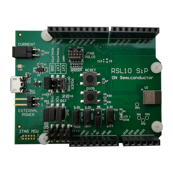
- Page 1 I/O signal level of the Development Board Design ♦ RSL10 SIP to the 3.3 V digital logic level. It is not enabled Power Supply ♦ by default; you enable it when it is needed.
- Page 2 Figure 3 shows the locations of the various The following sections detail the various sub-circuits of circuit sections. Figure 5 Figure 6 provide the RSL10 SIP Evaluation and Development Board. The 3-dimensional illustrations of the SiP board. www.onsemi.com Arrow.com. Arrow.com. Downloaded from Downloaded from...
- Page 3 EVBUM2565/D Figure 3. Circuit Location Block Diagram (Top View) Figure 4. Circuit Location Block Diagram (Bottom View) www.onsemi.com Arrow.com. Arrow.com. Arrow.com. Downloaded from Downloaded from Downloaded from...
- Page 4 EVBUM2565/D Figure 5. Three-Dimensional Line Drawing of the Board (Top View) Figure 6. Three-Dimensional Line Drawing of the Board (Bottom View) www.onsemi.com Arrow.com. Arrow.com. Arrow.com. Arrow.com. Downloaded from Downloaded from Downloaded from Downloaded from...
- Page 5 (MCU). The other is the green LED, The board has level translators for the DIO signals of the connected to DIO 6 of RSL10 SIP. You can use this LED RSL10 SIP, including the clock signal. The level translators...
- Page 6 9-pin 0.05 in Samtec FTSH header ( ), defined by the AD1, IOL1, and IOH1). Arm Cortex−M3 core on the board, connects RSL10 SIP to The LED circuit provides visual monitoring of the DIOs; external adapters compatible with the Arm Cortex−M3 refer to Section “LED Circuitry”...
-
Page 7: Appendix A − Connectors
Current measurement header External power supply header Input and output of level shifter Switches Table 5. SWITCH DESCRIPTIONS Designator Description Pushbutton switch to reset RSL10 SIP Pushbutton switch for DIO5 Connectors Table 6. CONNECTOR DESCRIPTIONS Designator Description RF switch connector... -
Page 8: Appendix B − Schematics
EVBUM2565/D APPENDIX B − SCHEMATICS This appendix contains schematics for the Evaluation and Development Board, version 1.3: • The Top-level (Arduino interface) schematic • The RSL10 SIP schematic • The Interface MCU schematic • The Power Supply schematic RESET TRESin... - Page 9 EVBUM2565/D VBAT VDDO Figure 8. RSL10 SIP Schematic www.onsemi.com Arrow.com. Arrow.com. Arrow.com. Arrow.com. Arrow.com. Arrow.com. Arrow.com. Arrow.com. Arrow.com. Downloaded from Downloaded from Downloaded from Downloaded from Downloaded from Downloaded from Downloaded from Downloaded from Downloaded from...
- Page 10 EVBUM2565/D DHSDP XIN32 DHSD_P DHSDM XOUT32 DHSD_N JTAGSEL NRSTB VDDUTMI DFSDM GNDBU DFSD_N VDDBU DFSDP DFSD_P GNDUTMI TEST ERASE VDDCORE FWUP TK/PWMH0/PA28 RK/PWMH1/PA29 PA12/UTXD/PWMFI1 RF/TIOB2/PA31 PA11/URXD/PWMFI0 PA10/TWCK0/PWML3 VDDCORE VDDIO PA9/TWD0/PWML2 PA8/MCDA3/PWML1 VDDIO PWMH0/A2/PB0 PWMH1/A3/PB1 PWMH2/A4/PB2 VDDCORE PA7/MCDA2/PWML0 D2/DCD0/PB11 PA6/MCDA1/PWMH2 D3/RI0/PB12 D4/PWMH0/PB13 PA5/MCDA0/PWMH1 PA4/MCCDA/PWMH0...
- Page 11 EVBUM2565/D Figure 10. Power Supply Schematic www.onsemi.com Arrow.com. Arrow.com. Arrow.com. Arrow.com. Arrow.com. Arrow.com. Arrow.com. Arrow.com. Arrow.com. Arrow.com. Arrow.com. Downloaded from Downloaded from Downloaded from Downloaded from Downloaded from Downloaded from Downloaded from Downloaded from Downloaded from Downloaded from Downloaded from...
-
Page 12: Appendix C − Bill Of Materials
EVBUM2565/D APPENDIX C − BILL OF MATERIALS Table 7. BILL OF MATERIALS FOR RSL10 SIP EVALUATION AND DEVELOPMENT BOARD VERSION Designator Description Footprint Doc Arduino Stackable Header 6-pin C9, C40, C43 CAP CER 4.7 mF 10 V X5R 0603, CAP CER 4.7 mF 25 V X5R... - Page 13 FDA Class 3 medical devices or medical devices with a same or similar classification in a foreign jurisdiction or any devices intended for implantation in the human body. Should Buyer purchase or use ON Semiconductor products for any such unintended or unauthorized...
Need help?
Do you have a question about the RSL10 SIP and is the answer not in the manual?
Questions and answers