Table of Contents
Advertisement
Quick Links
Advertisement
Table of Contents

Related Manuals for Texas Instruments DAC8541EVM


Summary of Contents for Texas Instruments DAC8541EVM
- Page 1 DAC8541EVM User’s Guide August 2002 Data Acquisition SLAU085A...
- Page 2 IMPORTANT NOTICE Texas Instruments Incorporated and its subsidiaries (TI) reserve the right to make corrections, modifications, enhancements, improvements, and other changes to its products and services at any time and to discontinue any product or service without notice. Customers should obtain the latest relevant information before placing orders and should verify that such information is current and complete.
- Page 3 EVM IMPORTANT NOTICE Texas Instruments (TI) provides the enclosed product(s) under the following conditions: This evaluation kit being sold by TI is intended for use for ENGINEERING DEVELOPMENT OR EVALUATION PURPOSES ONLY and is not considered by TI to be fit for commercial use. As such, the goods being provided may not be complete in terms of required design-, marketing-, and/or manufacturing-related protective considerations, including product safety measures typically found in the end product incorporating the goods.
- Page 4 EVM schematic located in the EVM User’s Guide. When placing measurement probes near these devices during operation, please be aware that these devices may be very warm to the touch. Mailing Address: Texas Instruments Post Office Box 655303 Dallas, Texas 75265 Copyright 2002, Texas Instruments Incorporated...
- Page 5 Information About Cautions and Warnings Preface Read This First About This Manual This user’s guide describes the characteristics, operation, and the use of the DAC8541 evaluation module. It covers all pertinent areas involved to properly use this EVM board along with the devices that it supports. The physical PCB layout, schematic diagram and circuit descriptions are included.
- Page 6 Trademarks The TI Logo is a trademark of Texas Instruments Incorporated. SPI and QSPI are trademarks of Motorola, Inc.
-
Page 7: Table Of Contents
Contents Contents EVM Overview ..............Features . - Page 8 Contents Figures 1 - 1. EVM Block Diagram ............2 - 1.
-
Page 9: Evm Overview
Chapter 1 EVM Overview This chapter gives a general overview of the DAC8541EVM and describes some of the factors that must be considered in using this module. Topic Page Features ........... . . -
Page 10: Features
1.1 Features This EVM features the DAC8541 digital-to-analog converter. The DAC8541EVM is a simple evaluation module designed for a quick and easy way to evaluate the functionality of the high resolution, single-channel, parallel input DAC. This EVM features a parallel interface to communicate to any host processor base system. -
Page 11: Evm Basic Functions
5 V maximum. Otherwise, this damages U1 part, DUT. 1.3 EVM Basic Functions The DAC8541EVM is a functional evaluation platform to test certain functional characteristics of the DAC8541 digital-to-analog converter. Functional evaluation of the DAC device can be accomplished with the use of any microprocessor, DSP, or some sort of a waveform generator. - Page 12 EVM Basic Functions Figure 1 - 1. DAC8541EVM Block Diagram 15 V 15 V - 15 V (J6) - 15 V (J7) Reference Module Output Buffer Module LDAC DAC Out Ext. Ref. Input (J6) RSTSEL (J7) (J1) BTC/USB DAC Module...
-
Page 13: Physical Description
Chapter 2 Physical Description This chapter describes the physical characteristics and PCB layout of the EVM and lists the components used on the module. Topic Page PCB Layout ..........Bill of Materials . -
Page 14: Pcb Layout
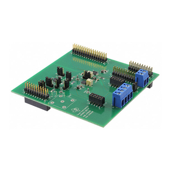
PCB Layout 2.1 PCB Layout The DAC8541EVM is constructed on two-layer printed-circuit board using a copper-clad FR-4 laminate material. The printed-circuit board has a dimension of 99,06 mm (3.90 inch) × 104, 14 mm (4.10 inch), and the board thickness is 1,57 mm (0.062 inch). -
Page 15: Layer Two (Bottom Layer)
PCB Layout Figure 2 - 2. Layer Two (Bottom Layer) Physical Description... -
Page 16: Drill Drawing
PCB Layout Figure 2 - 3. Drill Drawing... -
Page 17: Bill Of Materials
33 Ω, 1/4 W, 1206 chip resistor Panasonic ERJ-8GEYJ330V Bourns 3214W-104E 100 kΩ, BOURNS_32X4W series 5T J5 (see Note) AMP (Tyco) 227699-2 PCB mounted BNC—amphenol Texas Instruments DAC8541 16-bit, 32-TQFP DAC Lumberg KRMZ2 2-pin terminal screw connector Lumberg KRMZ4 4-pin terminal screw connector Texas Instruments... -
Page 19: Evm Operation
Chapter 3 EVM Operation This chapter covers the operation of the DAC8541EVM and provides guidance to the user in evaluating the onboard DAC and interfacing the EVM to a specific host processor. For information about its parallel interface and other related topics, refer to the DAC8541 data sheet, TI literature number SLAS353. -
Page 20: Factory Default Setting
Factory Default Setting 3.1 Factory Default Setting The EVM board is set as default from the factory to the configuration below to operate in bipolar mode through U2. Table 3 - 1. Factory Default Jumper Setting Reference Jumper Position Function 1 - 2 tied to AGND REF(L) -
Page 21: Output Gain Of Two
Host Processor Operation Table 3 - 2. Unity Gain Output Jumper Settings Reference Jumper Position Function 2 - 3 Negative rail of the op amp tied to analog GND Don’t care Positive rail of the op amp can be supplied by 15 V or V 3 - 4 Buffered output of DAC is channeled to the output terminals Open... -
Page 22: Bipolar Operation Using The Dac8541 (Default Mode)
Host Processor Operation Table 3 - 4. Capacitive Load Drive Output Jumper Settings Reference Jumper Position Function 2 - 3 Negative rail of the op amp tied to analog GND 1 - 2 Positive rail supply of the op amp tied to 15 V 3 - 4 Capacitive load drive output of DAC is channeled to the output terminals Open... -
Page 23: Dac8541 Bipolar Output Of Operation
Host Processor Operation 0000h corresponding to a - 5 V output and FFFFh corresponding to a 5 V output when BTC/USB = 0. If BTC/USB = 1, 8000h corresponds to - 5 V output and 7FFFh corresponds to 5 V output. Bipolar zero is given by the code 0000h applied to the DAC. -
Page 24: Jumper Setting Reference
Jumper Setting Reference 3.3 Jumper Setting Reference The illustrations in Table 3 - 6 shows the function of each jumper on the DAC8541EVM. Table 3 - 6. Jumper Setting Function Reference Jumper Setting Function tied to AGND REF(L) Enables V... -
Page 25: Schematic Diagram
Schematic Diagram 3.4 Schematic Diagram This section contains the schematic diagram for the DAC8541EVM. EVM Operation... - Page 26 Revision History ECN Number Approved LDAC RSTSEL BTC/USB DB15 11 12 11 12 DB14 13 14 13 14 LDAC DB13 LDAC 15 16 15 16 DB12 17 18 17 18 DB11 19 20 19 20 DB10 RSTSEL Male Header (TSM Series) Male Header (TSM Series) RSTSEL BTC/USB...
Need help?
Do you have a question about the DAC8541EVM and is the answer not in the manual?
Questions and answers