Table of Contents
Advertisement
Quick Links
This user's guide describes the characteristics, operation, and use of the ADS8380
18-bit, 600-kHz, high-speed, serial interface analog-to-digital converter evaluation
board (EVM). A complete circuit description, schematic diagram, and bill of materials
are included.
The following related documents are available on the TI Web site at www.ti.com.
Data Sheets:
ADS8380
REF1004C-2.5
SN74AHC1G125
THS4031
OPA132
1
2
3
4
5
6
8
9
1
.....................................................................................................................
2
3
4
5
1
Analog Input Connector
2
3
4
5
Power Connector J2 Pinout
7
ADS8380EVM Bill of Materials
SLAU146 - December 2004
Literature Numbers:
SLAS387
SBVS002
SCLS377
SLOS224
SBOS054
...............................................................................................................
..............................................................................................................
..............................................................................................................
..............................................................................................................
...............................................................................................................
............................................................................................
.................................................................................................................
..................................................................................................................
...........................................................................................................
................................................................................................................
...............................................................................................................
................................................................................................................
.....................................................................................................
...............................................................................................................
..................................................................................................
................................................................................................
.............................................................................................
Contents
List of Figures
List of Tables
...................................................................................
User's Guide
SLAU146 - December 2004
ADS8380EVM
ADS8380EVM
2
2
4
5
6
7
9
13
3
9
10
11
12
2
4
5
5
5
7
1
Advertisement
Table of Contents

Related Manuals for Texas Instruments ADS8380EVM


Summary of Contents for Texas Instruments ADS8380EVM
-
Page 1: Table Of Contents
Contents ....................... EVM Overview ......................Analog Interface ......................Digital Interface ......................Power Supplies ....................... Using the EVM .................... ADS8380EVM Bill Of Materials ......................... Board Layers ........................Schematics List of Figures ......................Input Buffer Circuit ........................Top Layer ........................ Power Plane ....................... -
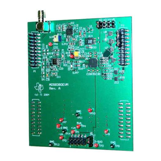
Page 2: Evm Overview
The amplifier circuit shown in Figure 1 is the buffer circuit used on the ADS8380EVM. This circuit consists of the THS4031, a high-speed, low-noise, low-distortion amplifier configured as an inverting gain of one. The circuit shown in Figure 1 was optimized to achieve the ac specifications (i.e., SNR, THD, SFDR, etc.) listed in the ADS8380 data sheet. -
Page 3: Input Buffer Circuit
The common SOIC footprint of U13 allows users to evaluate this converter with various reference ICs. The ADS8380EVM ships with the internal reference tied directly to the reference pin of the converter. SLAU146 – December 2004 ADS8380EVM... -
Page 4: Digital Interface
P1 and P2 to plug into prototype boards or through ribbon cable to user system boards. The digital input and output signals for the converter is available at connector P2 on the ADS8380EVM; Table 3 for the connector pinout. -
Page 5: Power Supplies
1-2 to select +5VD, or pins 2-3 to select +3.3VD as the source for the digital buffer voltage supply (+BVDD). Table 5. Power Connector J2 Pinout Signal J2 Pin Signal +VA(+12V) –VA(–12 V) +5VA DGND AGND +3.3VD +5VD SLAU146 – December 2004 ADS8380EVM... -
Page 6: Using The Evm
3. As a software test platform Reference Design As a reference design, the ADS8380EVM contains the essential circuitry to showcase the analog-to-digital converter. This essential circuitry includes the input amplifier, reference circuit, and buffers. The EVM analog-input circuit is optimized for a 100-kHz input signal; therefore, users may need to adjust the resistor and capacitor values to accommodate higher frequencies. -
Page 7: Ads8380Evm Bill Of Materials
ADS8380EVM Bill Of Materials ADS8380EVM Bill Of Materials The following table contains a complete bill of materials for the ADS8380EVM. The schematic diagram is also provided for reference. Contact the Product Information Center or email dataconvapps@list.ti.com questions regarding this EVM. - Page 8 ADS8380EVM Bill Of Materials Table 7. ADS8380EVM Bill of Materials (continued) Item Reference Manufacturer's Value Footprint Manufacturer Description Designator Part Number 1 µF TDK Corporation or C1608X5R1A105KT CAP CER 1 µF 10 V X5R 10% 0603 Alternate FERRITE CHIP 600 Ω 500 mA 0805...
-
Page 9: Board Layers
Board Layers Board Layers Figure 2. Top Layer SLAU146 – December 2004 ADS8380EVM... -
Page 10: Power Plane
Board Layers Figure 3. Power Plane ADS8380EVM SLAU146 – December 2004... -
Page 11: Ground Plane
Board Layers Figure 4. Ground Plane SLAU146 – December 2004 ADS8380EVM... -
Page 12: Bottom Layer
Board Layers Figure 5. Bottom Layer ADS8380EVM SLAU146 – December 2004... -
Page 13: Schematics
Schematics Schematics Schematic diagrams are appended following this page. SLAU146 – December 2004 ADS8380EVM... - Page 14 Serial Control +AVCC DGND AGND +3.3VD +5VD Power Supply +BVDD +BVDD +AVCC +AVCC Circuits 12500 TI Boulevard. Dallas, Texas 75243 TITLE: ADS8370EVM/ADS8380EVM Lijoy Philipose Engineer: DOCUMENT CONTROL #: REV: Lijoy Philipose 6458769 Drawn By: FILE: BlockDiagram.sch DATE: 30-Jun-2005 SIZE: SHEET:...
- Page 15 Revision History +VBD ECN Number Approved 0.1uF +5VCC B_SB/2C +VBD SN74X1G125 +VBD +VCC 0.1uF 0.1uF B_PD SJP1 SJP2 +VBD SN74X1G125 49.9 SB/2C SB/2C 0.1uF EXT_REF 47uF B_FS CONVST OPA132 +VBD SN74X1G125 CONVST +5VCC +5VCC SCLK SCLK 0.1uF +5VCC B_CS 1.2k 2.2uF 2.2uF SN74X1G125...
- Page 16 TI product or service and is an unfair and deceptive business practice. TI is not responsible or liable for any such statements. Following are URLs where you can obtain information on other Texas Instruments products and application solutions:...
Need help?
Do you have a question about the ADS8380EVM and is the answer not in the manual?
Questions and answers