Table of Contents
Advertisement
Quick Links
Advertisement
Table of Contents

Related Manuals for Texas Instruments ADS8364EVM


Summary of Contents for Texas Instruments ADS8364EVM
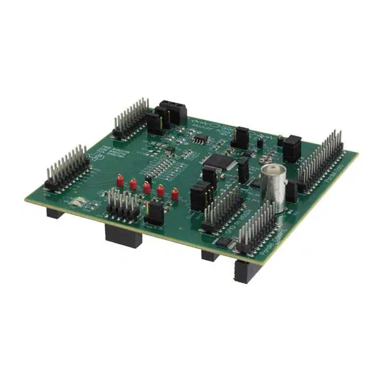
- Page 1 ADS8364EVM User’s Guide April 2002 Data Acquisition Products SLAU084...
- Page 2 IMPORTANT NOTICE Texas Instruments Incorporated and its subsidiaries (TI) reserve the right to make corrections, modifications, enhancements, improvements, and other changes to its products and services at any time and to discontinue any product or service without notice. Customers should obtain the latest relevant information before placing orders and should verify that such information is current and complete.
- Page 3 EVM IMPORTANT NOTICE Texas Instruments (TI) provides the enclosed product(s) under the following conditions: This evaluation kit being sold by TI is intended for use for ENGINEERING DEVELOPMENT OR EVALUATION PURPOSES ONLY and is not considered by TI to be fit for commercial use. As such, the goods being provided may not be complete in terms of required design-, marketing-, and/or manufacturing-related protective considerations, including product safety measures typically found in the end product incorporating the goods.
- Page 4 EVM schematic located in the EVM User’s Guide. When placing measurement probes near these devices during operation, please be aware that these devices may be very warm to the touch. Mailing Address: Texas Instruments Post Office Box 655303 Dallas, Texas 75265 Copyright 2002, Texas Instruments Incorporated...
- Page 5 Read This First About This Manual This users guide describes the characteristics, operation, and use of the ADS8364EVM 16-bit parallel analog-to-digital converter evaluation board. A complete circuit description as well as schematic diagram is included. How to Use This Manual This document contains the following chapters: Chapter 1—EVM Overview...
- Page 6 Related Documentation From Texas Instruments The information in a caution or a warning is provided for your protection. Please read each caution and warning carefully. Related Documentation From Texas Instruments To obtain a copy of any of the following TI documents, call the Texas Instruments Literature Response Center at (800) 477 - 8924 or the Product Information Center (PIC) at (972) 644 - 5580.
-
Page 7: Table Of Contents
Contents Contents EVM Overview ..............Analog Interface . - Page 8 2 - 1 ADS8364EVM Schematic—Analog Input Section ........
-
Page 9: Evm Overview
Chapter 1 EVM Overview The ADS8364 is a high-speed, low power, dual 16-bit A/D converter that operates from independent 5-V AV and DV supplies. The digital output is delivered through a built-in buffer circuit that can be powered from DV separate 2.7-V to 5.25-V (BV ) sources. -
Page 11: Analog Interface
Chapter 2 Analog Interface The analog portion of the board is divided in two parts. The input buffer represents the front-end circuit of the A/D converter. Its function is to provide level and impedance changes to the input signal. The second part is the voltage reference circuit. -
Page 12: Dual Supply-Input Buffer
2.1 Dual Supply—Input Buffer The analog input to the ADS8364EVM board is comprised of six independent OPA2132 operational amplifiers. The OPA2132s are powered from the ±12-V analog supply and connected as inverting amplifiers with a gain of 1. The internal 2.5-V reference voltage is applied to the noninverting input of the OPA2132s for level shifting. -
Page 13: Bipolar Inputs
2 - 3 2.3 Analog and Digital 5-V Supplies The ADS8364EVM board is configured at the factory for operation on the TMS320C6711 DSK platform. By default, W14 is open, which allows the DSP 5-V supply to be routed through U9 to the filter inductors L4 and L5. By closing W14, an external voltage source of 4.75 VDC to 5.25 VDC can be applied via... -
Page 14: Output Buffer 3.3-V Supply
2.4 Output Buffer 3.3-V Supply As mentioned above, the ADS8364EVM board is configured at the factory for operation on the TMS320C6711 DSK platform. Since the interface to this DSP is 3.3 V, the buffer supply voltage is taken from the DSP 3.3-V source found on the interface connector at J11 (pins 41 and 42). -
Page 15: Reference Voltage
W13 pins 2 and 3 (factory default). If an external reference is desired, the shunt jumper on W13 must be moved to cover pins 1 and 2. The ADS8364EVM provides two test-points, TP20 and TP22, as a means to connect an external source. An external source should be applied to TP20, referenced to TP22. -
Page 17: Digital Interface
Digital Interface The ADS8364 EVM is designed for easy interfacing with the C5000 and C6000 series DSK platforms from Texas Instruments. Two 80-pin interface connec- tors located on the bottom side of the EVM allow direct plug-in to the DSK plat- forms. -
Page 18: Control Signals
Control Signals 3.1 Control Signals The ADS8364EVM was developed on the TMS320C6711 DSK platform. The HOLDx signals, ADD pin control, and reset are all derived from the GPIO function of McBSP port 1. These signals are located on J12. The address and data lines are available on J11. -
Page 19: Power Supply
Chapter 4 Power Supply The power supply requirements for the ADS8364EVM board can be split into three categories—analog front end, ADC power, and digital interface. While filters are provided for all power supply inputs, optimal performance of the EVM requires a clean, well-regulated power source. -
Page 20: Analog Front-End Supply
Analog Front-End Supply 4.1 Analog Front-End Supply The analog front end of the EVM includes six OPA2132 operational amplifiers. These amplifiers are powered through J7 and are configured for bipolar operation. The circuits are designed to operate from a maximum supply voltage of ±12 VDC. -
Page 21: Adc Power Supply
ADC Power Supply 4.2 ADC Power Supply The ADS8364 requires analog and digital supplies in the range of 4.75 VDC to 5.25 VDC. The EVM provides both analog and digital supply voltages through a single input supply source. The 5-V input supply is filtered and split into the digital and analog power planes located on the inner layer of the PCB. -
Page 22: Digital Interface Supply
Digital Interface Supply 4.3 Digital Interface Supply A unique feature of the ADS8364 is the built-in data buffer circuit with an independent power source. The EVM provides a jumper—W18, which allows for flexible voltage selection. When the shunt at W18 is in the factory default position (W18 pins 2 and 3 shorted), the 3.3-V DSP supply taken from J11 is applied to the BV pins of the ADS8364. -
Page 23: Initial Setup Of The Board
330 pF 1 - 2 The analog inputs to the ADS8364EVM board can be applied to any one or all of the input channels. Single-ended inputs are to be applied between analog ground (center terminal of J1–J6) and either the positive or negative terminals. -
Page 25: Evm Schematic
Chapter 6 EVM Schematic The following pages contain the ADS8364EVM circuit diagram. EVM Schematic... - Page 26 Revision History ECN Number Approved Note: Components marked with asterisk are NOT installed! 330pF 330pF 330pF TP14 4.99K 4.99K 4.99K 4.99K 4.99K 4.99K -Vin -Vin -Vin A0In B0In C0In 49.9 49.9 49.9 OPA2132 OPA2132 OPA2132 100pF 100pF 100pF +Vin +Vin +Vin Vref Vref...
- Page 27 ADC Bypass BVdd DVdd AVdd AVdd DVdd BVdd 0.1uF 0.1uF 0.1uF 0.1uF 0.1uF 0.1uF 0.1uF DSP+5 DSP+12 DSP-12 DSP+5 TP35 DC_A17 DC_A16 DC_A15 DC_A14 TP28 RESET# DC_TOUT0 RESET# McBSP 1 Setup ADD = CLKX1 (GP OUT) HOLD A# = CLKR1 (GP OUT) 49.9 HOLD B# = FSX1 (GP OUT) DC_A5...
- Page 28 +VIN AVdd DSP+5 15uH + C22 33uF Green 4.7uH 0.1uF + C28 10uF 0.1uF /ENA DVdd TPS2104D Low = VIN1 TP21 4.7uH -VIN + C30 Green 10uF 0.1uF 15uH 33uF 0.1uF DVdd DSP+3.3 TP18 TP33 TP30 TP17 BVdd TP23 15uH 0 ohm + C23 33uF...
Need help?
Do you have a question about the ADS8364EVM and is the answer not in the manual?
Questions and answers