Advertisement
Quick Links
We have 45,000 LP502030-PCM-NTC-LD-A02554 - EEMB - Lithium Battery Rectangular 3.7V 250mAh Rechargeable in
stock now. Starting at $0.034. This EEMB part is fully warrantied and traceable.
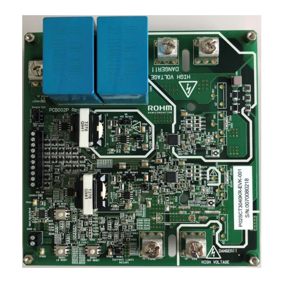
P02SCT3040KR-EVK-001
ROHM SEMICONDUCTOR
Buy Now
Looking for a discount?
Check out our current promotions!
This coversheet was created by Verical, a division of Arrow Electronics, Inc. ("Verical"). The attached document was created by the part supplier,
not Verical, and is provided strictly 'as is.' Verical, its subsidiaries, affiliates, employees, and agents make no representations or warranties
regarding the attached document and disclaim any liability for the consequences of relying on the information therein. All referenced brands,
product names, service names, and trademarks are the property of their respective owners.
00000005981LF-000
EOS Power
Buy Now
Give us a call
1-855-837-4225
International: 1-555-555-5555
1-415-281-3866
1-415-281-3866
Arrow Electronics,
Arrow Electronics, Inc
Verical Division
9201 East Dry Creek Road
P.O. Box 740970
Centennial, CO 80112
Los Angeles, CA 90074-0970
Advertisement

Related Manuals for Rohm TO-247-4L


Summary of Contents for Rohm TO-247-4L
- Page 1 We have 45,000 LP502030-PCM-NTC-LD-A02554 - EEMB - Lithium Battery Rectangular 3.7V 250mAh Rechargeable in stock now. Starting at $0.034. This EEMB part is fully warrantied and traceable. 00000005981LF-000 P02SCT3040KR-EVK-001 EOS Power ROHM SEMICONDUCTOR Buy Now Buy Now Looking for a discount? Check out our current promotions!
- Page 2 TO-247-4L Half-Bridge Evaluation Board Operation Manual...
-
Page 3: High Voltage Safety Precautions
[8] Be sure to wear insulated gloves when handling is required during operation. After Use [9] The ROHM Evaluation Board contains the circuits which store the high voltage. Since it stores the charges even after the connected power circuits are cut, please discharge the electricity after using it, and please deal with it after confirming such electric discharge. - Page 4 Gate signal protection circuit and so forth. In this application note the evaluation board operational guide for the TO-247-4L package will be explained. Additionally the detail information regarding topology, BOM, PCB layout, and electrical characteristics is described in the other application note. (TO-247-4L Half-bridge Evaluation Board Product Specification: No.62UG018E Rev.001)
-
Page 5: Led Indicators
TO-247-4L Half-Bridge Evaluation Board User’s Guide 2.LED Indicators In order to understand the operational condition of the board this evaluation board is equipped with several LED indicators. The location of the LEDs is shown in Figure 2, the indication details are described in Table 1 and LED status details for each occurred event are described in Table 2. - Page 6 TO-247-4L Half-Bridge Evaluation Board User’s Guide Table 1. LED Indication Indication Status Details ON when HVdc is over 10V. This LED may still ON even if the HVdc is switched off. Do not touch the board if this LED is ON.
- Page 7 TO-247-4L Half-Bridge Evaluation Board User’s Guide 3.OCP Setting 3.1 OCP Detection Signal Over Current Protection (OCP) circuit detects the voltage drop across the current sense resistor mounted between LS MOSFET Source and PGND, inputs the OCP detection signal to VTSIN input (pin 01) of LS MOSFET driver IC (U102), generates the FLT signal at the input signal side, and makes all the CLK signals invalid including at the HS side.
- Page 8 TO-247-4L Half-Bridge Evaluation Board User’s Guide OCP circuit configuration consists of transistors for start-up (Q301, Q305), transistor for Latch (Q303), transistor for Gate OFF (Q304), and transistor for LED indication (Q306). Furthermore, the resistors R362/R363 and R364/R365 to select the OCP circuit GND are available.
- Page 9 TO-247-4L Half-Bridge Evaluation Board User’s Guide JP51 CN201 HS_FAULT Reset switch JP151 HS_FAULT LS_FAULT LS_FAULT Reset switch CN202 OCP Reset switch TP303 RV301 TP302 Figure 4. Connector and OCP Adjustment Circuit © 2019 ROHM Co., Ltd. No. 61UG047E Rev.001 6/38...
- Page 10 TO-247-4L Half-Bridge Evaluation Board User’s Guide 3.2 Setting at Zero Bias OCP setting during zero bias is not possible. Thus, the OCP setting current I is estimated as below: = ((R361//R350)+R349)/R349*V /0.0047 = 171A BE_Q301 3.3 Setting at Negative Bias During negative bias, OCP point can be adjusted by adjusting the value of adjustable resistor RV301.
- Page 11 TO-247-4L Half-Bridge Evaluation Board User’s Guide The OCP start-up sequence example at negative bias is shown in Figure 5. OCP setting: 53A (Voltage between TP 303-TP302: 0.4V) OCP設定:53A(TP303-TP302間電圧:0.4V) ソフト Vgs_LS Soft-turn-OFF (TP151) ターンオフ Q301 Collector Q301コレクタ 2.31us 19.1us 7.37us (TP203) 0.58V...
-
Page 12: Connector Pin Assignments
TO-247-4L Half-Bridge Evaluation Board User’s Guide 4.Connector Pin Assignments Connectors’ pin assignment is shown in Figure 6. Each signal and power supply pin description are described in Table 6 and Table 7. Figure 6. Connector Pin Assignment Table 6. Power Supply Pin Description... - Page 13 TO-247-4L Half-Bridge Evaluation Board User’s Guide Connector Symbol Details CN201 ENABLE Driver ICs U2 and U102 shared Enable pin (individual control is not required) Active (Driver IC operates) when this signal is Low. It is being pulled up with 2.2kΩ resistor at +5V when OPEN.
- Page 14 TO-247-4L Half-Bridge Evaluation Board User’s Guide 5.CLK Select Function (JP201 Setting) It is important to prevent simultaneous activation of the HS and LS Gates of the MOSFETs when using a half-bridge configuration. For this evaluation board, selection between Single-CLK Mode that allows driving with a single external signal while preventing the HS and LS simultaneous ON condition, or Dual/DP-CLK Mode that allows ON/OFF driving individually is possible.
-
Page 15: Top View
6.Gate Drive Voltage Setting Gate drive voltage is supplied by the isolated type Flyback power supply mounted on the board. ROHM’s optocoupler-less control IC (BD7F200EFJ) is used for this Flyback power supply. In addition, transformers to output positive/negative drive voltage for each LS and HS are included. - Page 16 TO-247-4L Half-Bridge Evaluation Board User’s Guide 6.1 Positive Bias (VCC2) Adjustment Isolated Flyback power supply transformers (TX1, TX101) are used to generate both positive and negative voltages. The MOSFET drive voltage (positive bias) VCC2 is generated through a LDO Regulator from the transformer’s positive output. The LDO Output voltage is adjustable by adjusting the RV51 and RV151 resistor values.
- Page 17 Bias voltage during MOSFET OFF (negative bias VEE2) is stabilized at -2V from the negative voltage of TX1 and TX101 transformers by using ZD51 and ZD151 Zener diodes (ROHM: TFZVTR2.0B). VEE2 is supplied through JP51 and JP151 negative bias setting pins.
- Page 18 The drive circuit mounting condition is shown in Figure 10, and the circuit diagram is shown in Figure 11. The MOSFET is driven by ROHM’s MOSFET driver IC (BM6101FV-C) output signal through the Gate resistors. It is better to shorten the wiring of the driver circuit pattern as it’s inductance affects the surge voltage characteristics of the Gate-Source signal.
- Page 19 TO-247-4L Half-Bridge Evaluation Board User’s Guide Furthermore, switching speed adjustment can also be done by using either D51 (D151) or D52 (D152). For example, to set the turn ON slower, use D52 (D152) for diodes, and R73 (R173), R74 (R174), R75 (R175) for resistors. Here, the total gate Resistances are R73 (R173) + R74 (R174) // R75 (R175) for the turn ON, and R74 (R174) // R75 (R175) for the turn OFF.
- Page 20 TO-247-4L Half-Bridge Evaluation Board User’s Guide A specific example of the adjustment is shown in Table 10. However, there are also adjustments other than the example shown in the Table 10. Table 10. Gate Drive Speed Adjustment Gate Drive Circuit Resistor and Diode (Mount/No Mount)
- Page 21 TO-247-4L Half-Bridge Evaluation Board User’s Guide PROUT GND1 100 Ω BM6101FV- VEE2 OUT1 VCC2 FILTERS 0.1uF 3.3Ω VREG VCC1 OUT2 SCPIN GND2 47k Ω CX51 0 Ω TEST VEE2 VTSIN GND1 4.7kΩ VEE2 1000pF 0.1uF Vcc2 Slower Turn-On, Faster Turn-Off...
- Page 22 TO-247-4L Half-Bridge Evaluation Board User’s Guide 8.Dead Time Adjustment Although HS and LS ON/OFF by IN_CLK signal is possible when 「Single-CLK」 Mode is selected from CLK Select function, it is important to prevent simultaneous turn ON of HS and LS. Therefore, a dead time in which both the HS and LS are OFF needs to be included.
-
Page 23: Source Side
TO-247-4L Half-Bridge Evaluation Board User’s Guide 9.Device Current Measurement There are two through-holes (no plating) for each HS and LS on this evaluation board to allow the current flowing to each device to be easily measured using a Rogowski current probe. It is possible to measure the current at the Drain pin for the HS and at the Power Source pin for the LS. - Page 24 TO-247-4L Half-Bridge Evaluation Board User’s Guide Rogowski current probes have various loop diameters, the suitable diameter for this evaluation board is shown in Figure 1, 25mm~30mm for the circle diameter, and less than 3mm for the wire diameter. The dimension of the through-holes is shown in Figure 17.
- Page 25 DUT with evaluation environment under the same conditions. Shared drive circuit (HS) is shown in Figure 18. Q51 is for TO-247-4L and Q52 is for TO-247N. Each pin is connected, but the Q52 Gate circuit return line (return loop to GND2) is separated by R77 resistor (R177 for LS) to avoid the merging of Power Source pin and return line when 4L DUT is mounted.
-
Page 26: Heat Sink Installation
TO-247-4L Half-Bridge Evaluation Board User’s Guide 11.Heatsink Installation When performing power conversion of several kW such as efficiency measurement based on a power supply topology, the device power consumption itself may reach several W, which will require a heatsink. The layout allows the using of a single heatsink for the cooling purpose even for the commutation devices. - Page 27 TO-247-4L Half-Bridge Evaluation Board User’s Guide Input Bulk Capacitor Inductor Heatsink Output Bulk Capacitor PWM Clock Figure 22. Heat Sink Installation 25 kHz Vin = 300V, Vout=600V 50 kHz 100 kHz 100 kHz 50 kHz 25 kHz 100 kHz 50 kHz 25 kHz Figure 23.
- Page 28 TO-247-4L Half-Bridge Evaluation Board User’s Guide 12.Evaluation Board Connection Example 12.1 Double-pulse Test for HS MOSFET The connection of the double-pulse test for HS MOSFET is shown in Figure 24. Dual / DP Jumper setting Single HVdc PRIMERY SECONDERY +12V...
- Page 29 TO-247-4L Half-Bridge Evaluation Board User’s Guide Usually, double-pulse signal is a single-shot, please insure adequate inductor current IDP reset time between pulses if a periodic pulse is applied. As the reset voltage is equal to freewheeling diode forward voltage VF, the reset time can be calculated using the...
- Page 30 TO-247-4L Half-Bridge Evaluation Board User’s Guide 12.3 Boost Topology Power Supply Circuit The connection of the boost operation by switching the LS MOSFET is shown in Figure 26. Dual / DP Jumper setting HVdc Single PRIMERY SECONDERY +12V Power Gate Power...
- Page 31 TO-247-4L Half-Bridge Evaluation Board User’s Guide 12.4 2Level Inverter Circuit Dual / DP 2 level inverter circuit based on half bridge configuration is shown in figure 27. Jumper setting Single HVdc PRIMERY SECONDERY +12V Gate Power PGND Power Supply SGND...
- Page 32 TO-247-4L Half-Bridge Evaluation Board User’s Guide 12.5 Synchronous Buck Topology Power Supply Circuit Dual / DP The connection of the buck operation using the HS MOSFET is shown in Figure 28. Jumper setting Single HVdc PRIMERY SECONDERY +12V Power Gate Power...
- Page 33 TO-247-4L Half-Bridge Evaluation Board User’s Guide At the CCM Mode in which the inductor current is continuous, the output voltage is approximately defined as below: Vout=Duty*Vin On the other hand, at the DCM Mode, output voltage becomes equal to the input voltage because it is an open loop control, and the pulse is not thinning-out, the output voltage is equal to the input voltage.
-
Page 34: Snubber Circuit
TO-247-4L Half-Bridge Evaluation Board User’s Guide 13.Snubber Circuit This evaluation board is equipped with non-discharge type RCD Snubber circuit layout for MOSFET turn OFF surge suppression, the circuit is shown in Figure 29. HVdc C5750C0G3A333J280KC 33nF 1000V 5750 SCT3030AW SCT3040KR... - Page 35 TO-247-4L Half-Bridge Evaluation Board User’s Guide Here, the L is the wiring inductance of the main circuit to the bulk (DC link) capacitor, I is the drain current during TRACE MAIN MOSFET turn OFF, and f is the switching frequency of the MOSFET.
- Page 36 MOSFET. Among ROHM SiC MOSFETs, the third generation SCT3xxxx Series has a narrow Gate-Source voltage rating thus, it is recommended to have these clamp circuits. The Vgs surge voltage can be more effectively suppressed by implementing several of them on the board, but the priority of the layout to be close to the MOSFET is as follows: (III)Active Clamp MOSFET ...
- Page 37 TO-247-4L Half-Bridge Evaluation Board User’s Guide BM6101FV PROUT GND1 100 Ω VEE2 OUT1 0.1uF VCC2 FILTERS VREG VCC1 3.3 Ω 3.3 Ω OUT2 SCPIN (IV) GND2 47k Ω ZD52 0 Ω (III) TEST VEE2 VTSIN GND1 0 Ω (II) ZD53...
- Page 38 TO-247-4L Half-Bridge Evaluation Board User’s Guide ■ Waveform example when clamp-SBD is used Figure 33 shows the Vgs surge suppression effect at double pulse test when clamp SBD is used. SCT3040KR MOSFETs are connected in a half-bridge configuration and switching is done on the high side MOSFET. The external Gate resistor is 10Ω. From top, the first waveform is the high side MOSFET Vgs, the second waveform is the commutation side (low side) Vgs, the third waveform is the high side Vds, and the last waveform is the high side Id.
- Page 39 TO-247-4L Half-Bridge Evaluation Board User’s Guide ■Waveform comparison by using different Cgs capacitances(Without protection circuit) Figure 34 shows the measurement result and the effect of using Cgs on the self-turn on and surge voltage. From the waveforms, we can see that the self-turn on can be prevented by adding the Cgs. However, we also understand that the Cgs does not give a significant effect on the negative surge at turn off.
- Page 40 TO-247-4L Half-Bridge Evaluation Board User’s Guide ■Waveform comparison by using different Cgs capacitances(With protection circuits) Finally, the measured waveforms when all the Vgs protection circuits are applied are shown in Figure 35. All the abnormalities during turn on and turn off disappeared, therefore, Cgs is not needed.
- Page 41 TO-247-4L Half-Bridge Evaluation Board User’s Guide 15.Precautions when measuring the Gate-Source signal Drain current di/dt of the MOSFETs with driver source pin is in several A/ns level. Thus, the generation of radiation noise is quite big. Therefore, pay attention to the connection of the voltage probes when measuring comparatively low voltage signals. Figure 36 shows the influence of the voltage probe connection on the measured waveforms.
- Page 42 Products. ROHM does not grant you, explicitly or implicitly, any license to use or exercise intellectual property or other rights held by ROHM or any other parties. ROHM shall have no responsibility whatsoever for any dispute arising out of the use of such technical information.
Need help?
Do you have a question about the TO-247-4L and is the answer not in the manual?
Questions and answers