Table of Contents
Advertisement
Quick Links
Power Management IC designed for "NXP
BD71837MWV Platform Design Guide
1. Introduction
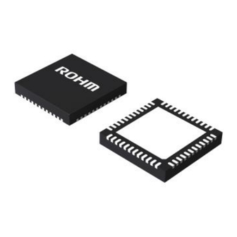
BD71837MWV is a Power Management Integrated Circuit (PMIC) available in 68-QFN package and dedicated to the application
powered by 5V input. PMIC includes eight Buck convertors, seven LDOs, one internal load switch and crystal oscillator driver for RTC
clock. These functions are designed to support the specific power requirements from NXP i.MX 8M platform to achieve the required
performance for cost-sensitive applications.
The below figure is the outline of the power map between PMIC and i.MX 8M SoC, showing that all voltage rails required by SoC are
satisfied.
"BD71837MWV Platform Design Guide" provides the guideline for designing PCB including recommendation for the PCB layer stack
up, the components placement and the PCB routings.
To reduce the risk that comes from PCB layout or parts placement, the guideline is strongly recommended to be applied to the PCB
design.
USB /
BUCK1 0.9V / 3.6A
Li-Ion Battery
BUCK2 1.0V / 4.0A
2.7V to 5.5V
BUCK3 1.0V / 2.1A
BUCK4 1.0V / 1.0A
LDO1 3.3V / 10mA
LDO2 0.9V / 10mA
LDO7 3.3V / 150mA
BUCK6 3.3V / 3.0A
BUCK7 1.8V / 1.5A
BUCK5 1.0V / 2.5A
BUCK8 1.1V / 3.0A
VR Fault
UVLO
Die temp
Power On Key
Power On Key
Detection
Figure 1.1 The system power map
© 2018 ROHM Co., Ltd.
®
i.MX 8M Quad"
BD71837MWV
LDO3 1.8V / 150mA
LDO5 1.8V / 300mA
LDO4 0.9V / 250mA
LDO6 0.9V / 300mA
Power Mux Switch
1.8V/3.3V / 150mA
32.768kHz Crystal Oscillator Driver
I2C (slave)
Power
Power Mode
Sequencing
Control Signals
Controller
Interrupt
Application Note
i.MX 8M Quad
i.MX 8M QuadLite
i.MX 8M Dual
LPDDR4 Memory
SD Card
1/46
Figure 1.2 The package image
No. 61AN002E Rev.001
May.2018
Advertisement
Table of Contents

Related Manuals for Rohm BD71837MWV


Summary of Contents for Rohm BD71837MWV
-
Page 1: Introduction
1. Introduction BD71837MWV is a Power Management Integrated Circuit (PMIC) available in 68-QFN package and dedicated to the application powered by 5V input. PMIC includes eight Buck convertors, seven LDOs, one internal load switch and crystal oscillator driver for RTC clock. -
Page 2: Table Of Contents
Overall Component Placement ..........................20 5.2.2. Large Current Loop ..............................21 5.2.3. Power GND ................................22 5.2.4. VSYS (Power supply for BD71837MWV analog circuit) .................... 22 5.2.5. Other Signal Pattern Precautions ..........................22 5.2.6. Feedback Sense Lines .............................. 22 5.2.7. - Page 3 BD71837MWV Platform Design Guide Application Note 5.3.5.1. Schematic Example ............................... 30 5.3.5.2. Schematic Checklist ............................... 31 5.3.5.3. Layout Example ..............................32 5.3.6. BUCK6 (NVCC_3P3) ..............................32 5.3.6.1. Schematic Example ............................... 32 5.3.6.2. Schematic Checklist ............................... 33 5.3.6.3. Layout Example ..............................33 5.3.7.
-
Page 4: Revision History
BD71837MWV Platform Design Guide Application Note 2. Revision History Table 2.1 Revision History Revision Number Description Revision Date Initial release May. 1 , 2018 © 2018 ROHM Co., Ltd. No. 61AN002E Rev.001 4/46 May.2018... -
Page 5: Features
BD71837MWV Platform Design Guide Application Note 3. Features 3.1. Terminologies Table 3.1 Acronyms, Conventions and Terminologies Term Definition Bill Of Materials PMIC Power Management Integrated Circuit Field Effect Transistor Inter-Integrated Circuit Interrupt ReQuest Low Drop-Out Regulator Over Current Protection Over Voltage Protection System-On-a-Chip 3.2. -
Page 6: Pmic Futures
Application Note 3.3. PMIC futures BD71837MWV supply the power required by SoC and peripheral devices for NXP i.MX 8M platform. Once PMIC powered up, it can be controlled by I2C interface to determine the internal register settings. The followings explain the features incorporated in the IC. -
Page 7: General Design Considerations
BD71837MWV Platform Design Guide Application Note 4. General Design Considerations This chapter provides general PCB design guidelines such as BD71837MWV general parts placement. 4.1. Package Dimension of BD71837MWV ROHM B D 7 1 8 3 7 Part Number Marking LOT Number Figure 4.1 The package dimension of BD71837MWV... -
Page 8: Pin Configuration
BD71837MWV Platform Design Guide Application Note 4.2. Pin Configuration The pin configuration of BD71837MWV is designed and it will result in the effective routings between PMIC and SoC, memory device and other components. (**)EXP-PAD VIN_1P8_1 LDO6_VOUT SD_VSELECT PMIC_ON_REQ BUCK6_FB PMIC_STBY_REQ... -
Page 9: General Stack-Up Recommendations
Large metal area also reduces stray resistance and inductance. 4.4. 6-layer Board Stack-up BD71837MWV ROHM’s EVM uses Type 3 PCB technology and Figure 4.3 shows the 6-layer PCB stack-up. Figure 4.3 6-layers PCB stack-up © 2018 ROHM Co., Ltd. -
Page 10: Via Guidelines
Type-3 PCB technology employs plated through-hole (PTH) vias for breakout routing. The dimension of PTH vias may vary as necessary. Table 2.1 shows the recommended via dimension used for the breakout areas of BD71837MWV. Figure 4.4 shows the image of PTH vias. -
Page 11: Placement Of Pths Underneath The Exposed Pad
When the distance between the edge of metal mask of the exposed pad and PTH is close, the solder may get on the resist then the PTH and exposed pad of BD71837MWV will be shorted. To avoid the soldering issue, it is highly recommended to keep the positons of PTHs away from the edge of the exposed pad by 500μm or more, and PTHs should be placed not to disrupt the current flows... -
Page 12: Outline For Pcb Layout
Application Note 4.7. Outline for PCB layout For understanding the outline of ROHM’s reference layout, the layout data for Layer 1(Top Layer) to 6 (Bottom layer) are shown in Figure 4.6 to Figure 4.11. The layout is designed, supposing the position of the SoC as Figure 4.6. - Page 13 It’s better to secure the wide plane for large switching currents. The parasitic impedance between PGND and each capacitor should be as low as possible. Figure 4.7 BD71837MWV Reference Board Outline (Layer 2) © 2018 ROHM Co., Ltd. No. 61AN002E Rev.001 13/46 May.2018...
- Page 14 Layer 3 is used as VSYS power (Input for each VR). It’s better to secure the wide plane for large input currents which happens between input source and input capacitors. Figure 4.8 BD71837MWV Reference Board Outline (Layer 3) © 2018 ROHM Co., Ltd. No. 61AN002E Rev.001 14/46 May.2018...
- Page 15 Layer 4 is used as power traces for each VR. It’s better to secure the enough width to relief the effect of the parasitic impedance. Figure 4.9 BD71837MWV Reference Board Outline (Layer 4) © 2018 ROHM Co., Ltd. No. 61AN002E Rev.001 15/46 May.2018...
- Page 16 Layer 5 is used as the power traces for each LDO. It’s better to secure the enough width to relief the effect of the parasitic impedance. Figure 4.10 BD71837MWV Reference Board Outline (Layer 5) © 2018 ROHM Co., Ltd. No. 61AN002E Rev.001 16/46 May.2018...
- Page 17 BD71837MWV Platform Design Guide Application Note WDOG_B SD_VSELECT RTC_RESET_B IRQ_B POR_B C32K_OUT Layer 6 is used for routings of each feedback line and I/Os. Figure 4.11 BD71837MWV Reference Board Outline (Layer 6) © 2018 ROHM Co., Ltd. No. 61AN002E Rev.001 17/46 May.2018...
-
Page 18: Platform Power Delivery Guidelines
It is essential to follow the guidelines to ensure the stable power delivery to the SoC and the system. 5.1. Platform Power Delivery Figure 5.1 shows the voltages BD71837MWV provides to the SoC and other devices in the system and the information of the maximum currents for each VR are summarized in Table 5.1. - Page 19 1.5A, 1.6V to 2.0V / 8steps LDO4 0.9V 250mA, VDDA_0P9 0.9V to 1.8V LDO6 0.9V 0P9_PHY 300mA, 0.9V to 1.8V 1.8V 1.8V/3.3V(SD CARD) 150mA MUXSW 3.3V Figure 5.1 BD71837MWV Power Delivery Map © 2018 ROHM Co., Ltd. No. 61AN002E Rev.001 19/46 May.2018...
-
Page 20: General Layout Guideline
BD71837MWV Platform Design Guide Application Note 5.2. General Layout Guideline This section explains the guideline about the layout for voltage regulators. The voltage rails with higher Iomax current especially for BUCK convertors should be carefully designed not to transmit the unwanted interference caused by switching noises to other signals with high impedance. -
Page 21: Large Current Loop
BD71837MWV Platform Design Guide Application Note 5.2.2. Large Current Loop There are 2 high-pulsing current flow loops in the BUCK convertor system. Loop1 When Tr2 turns ON, the loop starts from the input capacitor, to VIN terminal, to LX terminal, to L (inductor), to output capacitors, and then returns to the input capacitor through GND. -
Page 22: Power Gnd
The enough numbers of vias for input capacitors should be used and the decoupling capacitors should be placed as close to PMIC as possible. The reference layout (BD71837MWV reference layout) can be referred to for your reference. BD71837MWV... -
Page 23: Agnd Layout
BD71837MWV Platform Design Guide Application Note 5.2.7. AGND layout Figure 5.6 Connection between Power GND and Analog GND AGND is recommended not to be connected to PGND for PMIC (exposed pad) directly to avoid noise effect. It’s better to short AGND to a GND at inner GND plane (stable GND) through PTH. -
Page 24: Buck Convertors
5.3. BUCK Convertors In this section, application circuits for each voltage rail are explained. For more detail information, the document of “BD71837MWV schematic check list” can be referred to. 5.3.1. BUCK1 (VDD_SoC) BUCK1 is a high-efficiency buck converter which converts VSYS (2.7V to 5.5V) voltage to a regulated voltage. -
Page 25: Parts Placement For Each Decoupling Capacitor
BD71837MWV Platform Design Guide Application Note 5.3.1.3. Parts placement for each decoupling capacitor About the parts placement for each capacitor around BUCK1, the below reference layout can be referred to. BUCK1_FB should be connected to near output capacitors. Output Cap... -
Page 26: Schematic Checklist
BD71837MWV Platform Design Guide Application Note 5.3.2.2. Schematic checklist Table 5.3 BUCK2 schematic checklist Pin Names Dir. Notes (Unit of parts size : mm) Check BUCK2 (VDD_ARM) Connect to the 5V power supply in the system. As a decoupling capacitor, use one 10μF. -
Page 27: Buck3 (Vdd_Gpu)
BD71837MWV Platform Design Guide Application Note 5.3.3. BUCK3 (VDD_GPU) BUCK3 is a high-efficiency buck converter which converts VSYS (2.7V to 5.5V) voltage to a regulated voltage. This VR can dynamically change its output voltage setting using the I2C interface. BUCK3 output voltage range is from 0.7V to 1.3V by 10mV step. -
Page 28: Layout Example
BD71837MWV Platform Design Guide Application Note 5.3.3.3. Layout Example About the parts placement for each capacitor around BUCK3, the below reference layout can be referred to. BUCK3_FB should be connected to near output capacitors. BUCK3_VIN BUCK3_LX Input Cap Inductor Output Cap... -
Page 29: Buck4 (Vdd_Vpu)
BD71837MWV Platform Design Guide Application Note 5.3.4. BUCK4 (VDD_VPU) BUCK4 is a high-efficiency buck converter which converts VSYS (2.7V to 5.5V) voltage to a regulated voltage. This VR can dynamically change its output voltage setting using the I2C interface. BUCK4 output voltage range is from 0.7V to 1.3V by 10mV step. -
Page 30: Layout Example
BD71837MWV Platform Design Guide Application Note 5.3.4.3. Layout Example About the parts placement for each capacitor around BUCK4, the below reference layout can be referred to. BUCK4_FB should be connected to near output capacitors. BUCK4_VIN BUCK4_LX Input Cap Inductor Output Cap... -
Page 31: Schematic Checklist
BD71837MWV Platform Design Guide Application Note 5.3.5.2. Schematic Checklist Table 5.6 BUCK5 schematic checklist Pin Names Dir. Notes (Unit of parts size : inch) Check BUCK5 (VDD_DRAM) Connect to the 5V power supply in the system. As a decoupling capacitor, use one 10μF. -
Page 32: Layout Example
BD71837MWV Platform Design Guide Application Note 5.3.5.3. Layout Example About the parts placement for each capacitor around BUCK5, the below reference layout can be referred to. BUCK5_FB should be connected to near output capacitors. BUCK5_LX Inductor Output Cap Feedback point... -
Page 33: Schematic Checklist
BD71837MWV Platform Design Guide Application Note 5.3.6.2. Schematic Checklist Table 5.7 BUCK6 schematic checklist Pin Names Dir. Notes (Unit of parts size : inch) Check BUCK6 (NVCC_3P3) Connect to the 5V power supply in the system. As a decoupling capacitor, use one 22μF. -
Page 34: Buck7 (Nvcc_1V8)
BD71837MWV Platform Design Guide Application Note 5.3.7. BUCK7 (NVCC_1V8) VBUCK7 is a high-efficiency buck converter which converts VSYS (2.7V to 5.5V) voltage to a regulated voltage. BUCK7 output voltage is programmable by the register and its range is from 1.6V to 2.0V by eight steps. -
Page 35: Layout Example
BD71837MWV Platform Design Guide Application Note 5.3.7.3. Layout Example About the parts placement for each capacitor around BUCK7, the below reference layout can be referred to. BUCK7_FB should be connected to near output capacitors. Feedback point Output Cap Inductor Input Cap... -
Page 36: Buck8 (Nvcc_Dram)
BD71837MWV Platform Design Guide Application Note 5.3.8. BUCK8 (NVCC_DRAM) BUCK8 is a high-efficiency buck converter which converts VSYS (2.7V to 5.5V) voltage to a regulated voltage. BUCK8 output voltage is programmable by the register and its range is from 0.8V to 1.4V by 10mV step. -
Page 37: Layout Example
BD71837MWV Platform Design Guide Application Note 5.3.8.3. Layout Example About the parts placement for each capacitor around BUCK8, the below reference layout can be referred to. BUCK8_FB should be connected to near output capacitors. Feedback point Output Cap Inductor Input... -
Page 38: Ldos
BD71837MWV Platform Design Guide Application Note 5.4. LDOs 5.4.1. LDO1 (NVCC_SNVS) VLDO1 converts VSYS (2.7V to 5.5V) voltage to a regulated voltage. LDO1 output voltage is programmable by the register and its range is from 3.0V to 3.3V or 1.6V to 1.9V by 100mV step. -
Page 39: Schematic Examples
BD71837MWV Platform Design Guide Application Note 5.4.8. Schematic Examples Figure 5.23 LDO1 to 7 Schematic Example 5.4.8.1. Schematic Checklist Table 5.10 LDO1-7 schematic checklist Pin Names Dir. Notes (Unit of parts size : mm) Check LDO1 (NVCC_SNVS) : Vout = 3.0V-3.3V / 1.6V-1.9V , Iomax=10mA As the output capacitor, use one 1μF capacitor. - Page 40 BD71837MWV Platform Design Guide Application Note Pin Names Dir. Notes (Unit of parts size : mm) Check LDO4 (VDDA_0P9) : Vout = 0.9V - 1.8V, Iomax=250mA As the output capacitor, use one 2.2μF capacitor. Select the output capacitors within the capacitance range defined in the datasheet of BD71837MWV.
-
Page 41: Load Sw
BD71837MWV Platform Design Guide Application Note 5.5. Load SW 5.5.1. MUXSW (NVCC_SD2) VMUXSW is the internal load switch for SD card power. MUXSW output voltage supports 1.8V and 3.3V which are determined by the setting of SD_VSELECT. 5.5.1.1. Schematic Examples Figure 5.24 MUXSW Schematic Example... -
Page 42: Crystal Oscillator Driver
C32K_OUT Connect to SoC Note: As the crystal oscillator for RTC clock circuit, 32.768 kHz and 12.5pF (KYOCERA) is used together with BD71837MWV evaluation board. It is recommended to tune the load capacitance finely in the actual set to guarantee the stable oscillation. -
Page 43: Layout Example
BD71837MWV Platform Design Guide Application Note 5.6.1.3. Layout Example Crystal oscillator driver circuit is extremely sensitive to external environment like parasitic capacitance due to the long wirings for XIN and XOUT. So it is recommended to position the Crystal oscillator part near PMIC to shorten the length of the wirings. -
Page 44: Interfaces
BD71837MWV Platform Design Guide Application Note 5.7. Interfaces I2C interface is selected for the communication between PMIC and SoC. 5.7.1. I2C Table 5.13 Schematic checklist of I2C Signal System Termination Pin Names Dir. Voltage Pull-up/Pull-down if it is not Notes... -
Page 45: System Control - Reset, Power, And Control Signals
BD71837MWV Platform Design Guide Application Note 5.7.2. System Control – Reset, Power, and Control Signals Table 5.14 Schematic checklist of System Control – Reset, Power, and Control Signals Expected Expected System Termination Signal Pin Names Dir. Pull-up/Pull-down if it is not... -
Page 46: Misc
BD71837MWV Platform Design Guide Application Note 5.7.3. MISC Table 5.15 Schematic checklist of MISC Signal Pin Names Dir. Notes Check Voltage Level MISC AGND Connect to PGND at inner GND plane EXP-PADs Connect to the inner GND plane with lower impedance (PGND0~4) Note: The package has one pad at bottom and four corner pads to fix the position of the part. - Page 47 Products. ROHM does not grant you, explicitly or implicitly, any license to use or exercise intellectual property or other rights held by ROHM or any other parties. ROHM shall have no responsibility whatsoever for any dispute arising out of the use of such technical information.
Need help?
Do you have a question about the BD71837MWV and is the answer not in the manual?
Questions and answers