Table of Contents
Advertisement
Quick Links
Advertisement
Table of Contents

Related Manuals for Acromag XMC-6VLX Series


Summary of Contents for Acromag XMC-6VLX Series
- Page 1 Artisan Technology Group is your source for quality new and certified-used/pre-owned equipment SERVICE CENTER REPAIRS WE BUY USED EQUIPMENT • FAST SHIPPING AND DELIVERY Experienced engineers and technicians on staff Sell your excess, underutilized, and idle used equipment at our full-service, in-house repair center We also offer credit for buy-backs and trade-ins •...
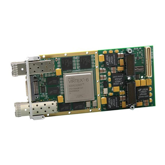
- Page 2 Virtex-6 Based FPGA XMC Module USER’S MANUAL ACROMAG INCORPORATED 30765 South Wixom Road P.O. BOX 437 Wixom, MI 48393-7037 U.S.A. Tel: (248) 295-0310 Copyright 2012, Acromag, Inc., Printed in the USA. Data and specifications are subject to change without notice. 8500-931C...
-
Page 3: Table Of Contents
Platform Flash Xilinx Configuration ......................15 BPI Flash Xilinx Configuration ........................15 PCIe CONFIGURATION ADDRESS SPACE ................16 CONFIGURATION REGISTERS ........................16 BAR0 MEMORY MAP ......................18 INTERRUPT CONTROLLER ....................19 Acromag, Inc. Tel: 248-295-0310 - 1 - - 1 - http://www.acromag.com www.acromag.com... - Page 4 System Monitor Status/Control Register (Read/Write) – (BAR0 + 0x300300) .......... 45 System Monitor Address Register (Write Only) – (BAR0 + 0x300304) ............45 Front Input Data Register (Read Only) - (BAR0 + 0x301000) ..............46 Acromag, Inc. Tel: 248-295-0310 - 2 - - 2 - http://www.acromag.com...
- Page 5 Host Peripherals............................65 Common Peripherals ..........................65 SDK ................................65 Acromag Peripheral Repository ......................... 67 Acromag modified library files ........................68 Running a Program from BPI FLASH Memory .................... 69 Running LWIP Echo Server ......................... 72 EDK File Organization ..........................74 Example EDK Design Modification Walkthrough ..................
- Page 6 It is important that you perform satisfactory overall system design and it is agreed between you and Acromag, that this is your responsibility. The information of this manual may change without notice. Acromag makes no warranty of any kind with regard to this material, including, but not limited to, the implied warranties of merchantability and fitness for a particular purpose.
-
Page 7: 1.0 General Information
The board will provide 2 Meg x 72-bit QDRII SRAM, 128 Meg x 64-bit DDR3 SDRAM, 4 Meg x 16-bit parallel Flash, and Xilinx 128 Megabit Platform Flash. The parallel Flash will interface to the FPGA for MicroBlaze CPU program Acromag, Inc. Tel: 248-295-0310 - 5 - - 5 - http://www.acromag.com... -
Page 8: Ordering Information
Interface to Rear P4 Connector – The Virtex 6 FPGA is directly connected to 64 pins of the rear P4 connector. All 2.5volt IO standards supported by the Virtex 6 device are available. The example design Acromag, Inc. Tel: 248-295-0310 - 6 - - 6 - http://www.acromag.com... -
Page 9: Pcle Interface Features
QDRII SRAM. Compatibility – PCI Express Base Specification v2.0 compliant PCI Express Endpoint. Provides one multifunction interrupt. The XMC-6VLX is compatible with XMC VITA 42.3 specification for P15. Acromag, Inc. Tel: 248-295-0310 - 7 - - 7 - http://www.acromag.com www.acromag.com... -
Page 10: Software
Acromag provides a software product consisting of board Linux software. This software (Model PMCSW-API-LNX) is composed of Linux libraries for all Acromag PMC, XMC, and VPX I/O board products, PCI and PCIe I/O cards, and CompactPCI I/O cards. The software supports X86 PCI bus only and is implemented as library of “C”... -
Page 11: 2.0 Preparation For Use
For repairs to a product damaged in shipment, refer to the Acromag Service Policy to obtain return instructions. It is suggested that salvageable shipping... -
Page 12: Default Hardware Configuration
Default Hardware Configuration The board may be configured differently, depending on the application. When the board is shipped from the factory, it is configured with the Acromag example design as follows: Slave SelectMap using Platform Flash (XCF128X) with onboard 48 MHz oscillator. -
Page 13: Rear P4 Field I/O Connector
RIO7_P RIO7_N connector. RIO8_P RIO8_N RIO9_P RIO9_N RIO10_P RIO10_N RIO11_P RIO11_N RIO12_P RIO12_N RIO13_P RIO13_N RIO14_P RIO14_N RIO15_P RIO15_N RIO16_P RIO16_N RIO17_P RIO17_N RIO18_P RIO18_N RIO19_P RIO19_N Acromag, Inc. Tel: 248-295-0310 - 11 - - 11 - http://www.acromag.com www.acromag.com... -
Page 14: Mezzanine Connector
FIO2_N FIO3_P FIO3_N Alternatively, 2.5volt LVDS I/O FIO4_P FIO4_N can be used on the front FIO5_P FIO5_N connector. FIO6_P FIO6_N FIO7_P FIO7_N FIO8_P FIO8_N FIO9_P FIO9_N FIO10_P FIO10_N Acromag, Inc. Tel: 248-295-0310 - 12 - - 12 - http://www.acromag.com www.acromag.com... -
Page 15: Non-Isolation Considerations
I/O grounds. As such, the field I/O connections are not isolated from the system. Care should be taken in designing installations without isolation to avoid noise pickup and ground loops caused by multiple ground connections. Acromag, Inc. Tel: 248-295-0310 - 13 - - 13 - http://www.acromag.com... -
Page 16: 3.0 Programming Information
If your code does not function as desired you may need to return to use of the Acromag design example. You can reload the Acromag example design via the EDK board and the JTAG port using the Xilinx iMPACT tool. -
Page 17: Virtex 6 Configuration
BPI Flash device. Registers are provided in the FPGA Programming Memory Map to implement BPI flash erase and reprogram operations. Acromag, Inc. Tel: 248-295-0310 - 15 - - 15 - http://www.acromag.com... -
Page 18: Pcie Configuration Address Space
Address Registers and the Interrupt Register which must be read to determine the base address assigned to the board and the interrupt request that goes active on a board interrupt request. Acromag, Inc. Tel: 248-295-0310 - 16 - - 16 - http://www.acromag.com... - Page 19 The PCIe bus decodes 4M bytes for BAR0 for this memory space. This board is also allocated a 16M byte block of memory (BAR2), to access QDRII memory. The PCIe bus decodes 16M bytes for BAR2 for this memory space. Acromag, Inc. Tel: 248-295-0310 - 17 - - 17 - http://www.acromag.com...
-
Page 20: Bar0 Memory Map
AXI CDMA (DS792) 0x000B0000→0x000EFFFF 256K Reserved 0x000F0000→0x000FFFFF PCIe AXI Bridge Control (DS820) 0x00100000→0x010FFFFF PCIe Interrupt Controller 0x00110000→0x002FFFFF Reserved Flash, I/O Reg, System Monitor, 0x00300000→0x0030FFFF and Aurora 0x00310000→0x003FFFFF Reserved Acromag, Inc. Tel: 248-295-0310 - 18 - - 18 - http://www.acromag.com www.acromag.com... -
Page 21: Interrupt Controller
Disabled Enabled This bit when set indicates an AXI CDMA interrupt. See the CDMA section for source of this interrupt. Disabled Enabled Reserved 31-2 Acromag, Inc. Tel: 248-295-0310 - 19 - - 19 - http://www.acromag.com www.acromag.com... -
Page 22: Interrupt Pending Register (Read) - (Bar0 + 0X00100004)
Interrupt Acknowledge Register, as described below. Reading this Interrupt Enable register indicates which interrupt inputs are enabled; where a ‘1’ indicates the input is enabled and a ‘0’ indicates the input is disabled. Acromag, Inc. Tel: 248-295-0310 - 20 - - 20 - http://www.acromag.com... -
Page 23: Interrupt Acknowledge Register (Write) - (Bar0 + 0X0010000C)
Writing 0s does nothing, as does wiring a ‘1’ to a bit location that corresponds to a non-existing interrupt input. The bit locations in the Set Interrupt Enable correspond with the bit locations given in the Interrupt Enable register Table. Acromag, Inc. Tel: 248-295-0310 - 21 - - 21 - http://www.acromag.com... -
Page 24: Clear Interrupt Enable Register (Write) - (Bar0 + 0X00100014)
Master IRQ Enable All Interrupts Disabled All Interrupts Enabled Hardware Interrupt Enable Software Interrupts Enabled Hardware Interrupts Only Enabled 31-2 Not Used (bits are read as logic “0”) Acromag, Inc. Tel: 248-295-0310 - 22 - - 22 - http://www.acromag.com www.acromag.com... -
Page 25: Axi-Cdma
Tail Descriptor Pointer Register 31:0 0x000A0014 Reserved 31:0 0x000A0018 Source Address Register 31:0 0x000A001C Reserved 31:0 0x000A0020 Destination Address Register 31:0 0x000A0024 Reserved 31:0 0x000A0028 Bytes to Transfer Register Acromag, Inc. Tel: 248-295-0310 - 23 - - 23 - http://www.acromag.com www.acromag.com... -
Page 26: Cdma Control Register (Read/Write) - (Bar0 + 0X000A0000)
Gather assisted transfers. Delayed Interrupt Disabled Delayed Interrupt Enabled Interrupt on Error Interrupt Enable. When set to ‘1’, it allows an error to generate an interrupt out. Error Interrupt Disabled Acromag, Inc. Tel: 248-295-0310 - 24 - - 24 - http://www.acromag.com www.acromag.com... - Page 27 CDMA has completed all scheduled work defined by the transfer descriptor chain (reached the tail pointer) and has not satisfied the Interrupt Threshold count. Note: Setting this value to zero disables the delay timer interrupt. Acromag, Inc. Tel: 248-295-0310 - 25 - - 25 - http://www.acromag.com www.acromag.com...
-
Page 28: Cdma Status Register (Read/Write) - (Bar0 + 0X000A0004)
AXI CDMA to gracefully halt. The CDMA Status register bit-1 is set to ‘1’ when the CDMA has completed shut down. A reset (soft or hard) must be issued to clear the error condition. Acromag, Inc. Tel: 248-295-0310 - 26 - - 26 - http://www.acromag.com... - Page 29 A reset (soft or hard) must be issued to clear the error condition. No Scatter Gather Decode Errors Scatter Gather Decode Error. CDMA Engine halts. Reserved Acromag, Inc. Tel: 248-295-0310 - 27 - - 27 - http://www.acromag.com www.acromag.com...
- Page 30 23-16 interrupt threshold value in the Scatter Gather Engine. Interrupt Delay Time Status. This field reflects the current 31-24 interrupt delay timer value in the Scatter Gather Engine. Acromag, Inc. Tel: 248-295-0310 - 28 - - 28 - http://www.acromag.com www.acromag.com...
-
Page 31: Cdma Current Descriptor Pointer Register (Read/Write) - (Bar0 + 0X000A0008)
On error detection, the Current Descriptor Pointer register is updated to reflect the descriptor associated with the detected error. Note: The register should only be written by the Software application when the AXI CDMA is Idle. Acromag, Inc. Tel: 248-295-0310 - 29 - - 29 - http://www.acromag.com www.acromag.com... -
Page 32: Cdma Tail Descriptor Pointer Register (Read/Write) - (Bar0 + 0X000A0010)
The software application must move the pointer to the last descriptor address it has updated. Acromag, Inc. Tel: 248-295-0310 - 30 - - 30 - http://www.acromag.com... -
Page 33: Cdma Source Address Register (Read/Write) - (Bar0 + 0X000A0018)
DMA operations as the starting write address for DMA data 31-0 transfers. Note: The software application should only write to this register when the AXI CDMA is Idle. Acromag, Inc. Tel: 248-295-0310 - 31 - - 31 - http://www.acromag.com www.acromag.com... -
Page 34: Cdma Bytes To Transfer Register (Read/Write) - (Bar0 + 0X000A0028)
6. Either poll the CDMA Status register bit-1 for logic ‘1’ or wait for the CDMA to generate an interrupt if enabled. 7. Clear the interrupt if generated by writing a ‘1’ to bit-12 CDMA Status Acromag, Inc. Tel: 248-295-0310 - 32 - - 32 - http://www.acromag.com... -
Page 35: Axi-Bar0 Aperture Base Address
AXI BAR0 Aperture Base address. The new AXI address is 0x01000000 + 0x00ABCDEF = 0x01ABCDEF. These values are then appended by the Virtex 6 hardware to give the final PCIe address of the system memory location. Acromag, Inc. Tel: 248-295-0310 - 33 - - 33 - http://www.acromag.com... -
Page 36: Pcie Axi-Bridge Control
Reports the current Link Training and Status State Machine state. Encoding is specific to the underlying Integrated Block. Reports the current lane reversal mode. No reversal 10-9 Lanes 1:0 reversed Lanes 3:0 reversed Lanes 7:0 reversed Acromag, Inc. Tel: 248-295-0310 - 34 - - 34 - http://www.acromag.com www.acromag.com... -
Page 37: Axi Base Address Translation Configuration Register (Read Only) - (Bar0 + 0Xf0208/0Xf020C)
This sets the system memory physical address which will be appended with the values written into either the DMA source or destination registers at 0xA0018 or 0xA0020 respectively. See the example in the CDMA section for additional details. Acromag, Inc. Tel: 248-295-0310 - 35 - - 35 - http://www.acromag.com... -
Page 38: Fpga Fabric Memory Map
Flash Data Register 24:0 0x300218 Flash Address Register 0x30021C→ 31:0 Reserved 0x3002FF 31:0 0x300300 System Monitor Status/Control Register 0x300304 31:0 System Monitor Address Register 0x300308→ 31:0 Reserved 0x300FFF Acromag, Inc. Tel: 248-295-0310 - 36 - - 36 - http://www.acromag.com www.acromag.com... -
Page 39: Front, Rear, And P16 I/O Registers (Read/Write) - (Bar0 + 0X301000 To 0X 301Fff)
Front write channel 0 interrupt status is identified via data bit-0 while front write channel 3 status is identified via data bit-3 of this register at BAR0 plus 0x300000. Acromag, Inc. Tel: 248-295-0310 - 37 - - 37 - http://www.acromag.com... -
Page 40: Ddr Memory Test Status Register (Read/Write) - (Bar0 + 0X300008)
The XMC Board Identification Code register at BAR0 plus 0x30000C stores an ID code that can used to uniquely identify the XMC Virtex 6 card. This register will read A3 hex as provided by the Acromag example design. The user can change the hardware setting of this register in the programmable FPGA code. -
Page 41: Aurora Monitor (Read/Write) - (Bar0 + 0X300104)
64K words deep. See the memory maps for both flash memory devices below. The least significant 16 bits A15 to A0 are used to select the 64K words of each block. Acromag, Inc. Tel: 248-295-0310 - 39 - - 39 - http://www.acromag.com... - Page 42 128 flash 64 Kword blocks as shown in this figure. A15 to A14 are used to select one of the four 16 Kword top blocks. Acromag, Inc. Tel: 248-295-0310 - 40 - - 40 - http://www.acromag.com www.acromag.com...
-
Page 43: Flash Status (Read Only) - (Bar0 + 0X300200)
Not Suspended Suspended Device Ready Status Device is busy Device is ready SR[6:1] are valid The Clear Status Register command is used to clear the Status Register error bits. Acromag, Inc. Tel: 248-295-0310 - 41 - - 41 - http://www.acromag.com www.acromag.com... -
Page 44: Flash Control (Write Only) - (Bar0 + 0X300204)
0x300208. Prior to issue of a Flash Read the Flash Address registers must be set with the desired address to be read. See the Flash Address registers at base address plus 0x300218. Acromag, Inc. Tel: 248-295-0310 - 42 - - 42 - http://www.acromag.com... -
Page 45: Flash Start Write (Write Only) - (Bar0 + 0X30020C)
Flash Address (Read/Write) – (BAR0 + 0x300218) This read/write register holds the address to which the flash chip is written upon issue of a flash start write command. Acromag, Inc. Tel: 248-295-0310 - 43 - - 43 - http://www.acromag.com... -
Page 46: Simple Bpi Flash Programming Example
9. Write 0x1 to address 0x30020C, flash data written to flash. 10. Write 0x0 to address 0x300218, set flash address back to 0. 11. Read address 0x300208, flash data at address 0x0 is 0x3AA3. Acromag, Inc. Tel: 248-295-0310 - 44 - - 44 - http://www.acromag.com... -
Page 47: System Monitor Status/Control Register (Read/Write) - (Bar0 + 0X300300)
Status Register 0x00 Temperature Register Map 0x01 Vccint 0x02 Vccaux 0x20 Maximum Temperature 0x21 Maximum Vccint 0x22 Maximum Vccaux 0x24 Minimum Temperature 0x25 Minimum Vccint 0x26 Minimum Vccaux Acromag, Inc. Tel: 248-295-0310 - 45 - - 45 - http://www.acromag.com www.acromag.com... -
Page 48: Front Input Data Register (Read Only) - (Bar0 + 0X301000)
0x301000. This front output data register is a read/writable register. Channel operations use 32-bit, 16-bit or 8-bit data transfers. All channels of this register are fixed as output channels. Acromag, Inc. Tel: 248-295-0310 - 46 - - 46 - http://www.acromag.com... -
Page 49: Front I/O Interrupt Enable Register (Read/Write) - (Bar0 + 0X301008)
For example, channel 0 is controlled via data bit-0. Bits 4 to 31 are not used and will always read as “0”. All bits are set to “0” following a reset which means that, if enabled, the Acromag, Inc. Tel: 248-295-0310 - 47 - - 47 - http://www.acromag.com... -
Page 50: Interrupt Polarity Register (Read/Write) - (Bar0 + 0X301010)
All bits are set to “0” following a reset, which means that the output will cause interrupts when they are logic low (provided they are enabled for interrupt on level). Acromag, Inc. Tel: 248-295-0310 - 48 - - 48 - http://www.acromag.com... -
Page 51: Rear Input Data Register (Read Only) - (Bar0 + 0X301100)
RI(18) RIO18_P RI(19) RIO19_P RI(20) RIO20_P RI(21) RIO21_P RI(22) RIO22_P RI(23) RIO23_P RI(24) RIO24_P RI(25) RIO25_P RI(26) RIO26_P RI(27) RIO27_P RI(28) RIO28_P RI(29) RIO29_P RI(30) RIO30_P RI(31) RIO31_GCLK_P Acromag, Inc. Tel: 248-295-0310 - 49 - - 49 - http://www.acromag.com www.acromag.com... -
Page 52: Rear Output Data Register (Read/Write) - (Bar0 + 0X301104)
RO(18) RIO18_N RO(19) RIO19_N RO(20) RIO20_N RO(21) RIO21_N RO(22) RIO22_N RO(23) RIO23_N RO(24) RIO24_N RO(25) RIO25_N RO(26) RIO26_N RO(27) RIO27_N RO(28) RIO28_N RO(29) RIO29_N RO(30) RIO30_N RO(31) RIO31_GCLK_N Acromag, Inc. Tel: 248-295-0310 - 50 - - 50 - http://www.acromag.com www.acromag.com... -
Page 53: P16 Input Data Register (Read Only) - (Bar0 + 0X301200)
P16_SI(5) P16_SIO6_N P16_SI(6) P16_SIO4_N P16_SI(7) P16_SIO2_N P16_SI(8) P16_SIO0_GCLK_N P16_SI(9) P16_SIO18_GCLK_P P16_SI(10) P16_SIO17_P P16_SI(11) P16_SIO15_P P16_SI(12) P16_SIO13_P P16_SI(13) P16_SIO11_P P16_SI(14) P16_SIO9_P P16_SI(15) P16_SIO7_P P16_SI(16) P16_SIO5_P P16_SI(17) P16_SIO3_P P16_SI(18) P16_SIO1_N Acromag, Inc. Tel: 248-295-0310 - 51 - - 51 - http://www.acromag.com www.acromag.com... -
Page 54: P16 Output Data Register (Write Only) - (Bar0 + 0X301204)
P16_SO(5) P16_SIO8_P P16_SO(6) P16_SIO6_P P16_SO(7) P16_SIO4_P P16_SO(8) P16_SIO2_P P16_SO(9) P16_SIO0_GCLK_P P16_SO(10) P16_SIO17_N P16_SO(11) P16_SIO15_N P16_SO(12) P16_SIO13_N P16_SO(13) P16_SIO11_N P16_SO(14) P16_SIO9_N P16_SO(15) P16_SIO7_N P16_SO(16) P16_SIO5_N P16_SO(17) P16_SIO3_N P16_SO(18) P16_SIO1_P Acromag, Inc. Tel: 248-295-0310 - 52 - - 52 - http://www.acromag.com www.acromag.com... -
Page 55: Bar2 Memory Map
QDR directly from the Virtex 6 FPGA. The memory device has a 2 Meg x 72- bits memory configuration. Reading or writing to this memory space using DMA access is also possible as 64-bit transfers. Acromag, Inc. Tel: 248-295-0310 - 53 - - 53 - http://www.acromag.com... -
Page 56: 4.0 Theory Of Operation
BPI Flash Memory pairs & (Bite-wide Peripheral Interface} 2 Global MicroBlaze CPU Instruction Storage Clock 16M x 16 = 256Mb or 32MB Pairs 64 pin Rear I/O Connector Acromag, Inc. Tel: 248-295-0310 - 54 - - 54 - http://www.acromag.com www.acromag.com... -
Page 57: Pci Interface Logic
XMC-6VLX USER’S MANUAL PCI INTERFACE LOGIC The Acromag example design PCIe bus interface logic on this board provides a 2.5Gbps interface to the carrier/CPU board per PCI Express Specification v2.0. The interface to the carrier/CPU board allows control of example design board functions. -
Page 58: Clock Generation
USB-to-UART Bridge The XMC-6VLX board contains a Silicon Labs CP2103GM USB-to-UART bridge device (U27) which allows connection from the Virtex 6 device to a host Acromag, Inc. Tel: 248-295-0310 - 56 - - 56 - http://www.acromag.com... -
Page 59: 16Mb Platform Flash
5 set On (closed) select the BPI Flash while Off (open) select the Platform Flash. The DIP switch selection can be overridden by the FPGA after configuration by controlling the logic level of the BPI_Flash net. Logic Acromag, Inc. Tel: 248-295-0310 - 57 - - 57 - http://www.acromag.com... -
Page 60: Configuration Flash Design Considerations
FPGA. Through the connection made by the temporary design in the FPGA, iMPACT can indirectly program the BPI flash or the Platform Flash from the JTAG port. Acromag, Inc. Tel: 248-295-0310 - 58 - - 58 - http://www.acromag.com... -
Page 61: Dip Switch
VPWR_5/12 pins. The VPWR_5/12 power is the V in voltage to the four LTM4602 devices U18, U19, U20, and U25. These LTM4602 devices output +1.0V, +1.5V, +2.5V and +1.8V voltages. The +1.5 V supply is input to both Acromag, Inc. Tel: 248-295-0310 - 59 - - 59 - http://www.acromag.com... - Page 62 +/-2 A TPS51120 QDRII+ Termination +0.75V_QDR +/-2 A LTM4602 VCCO, Flash +2.5V 6.0 A LTM4602 Flash, MGT +1.8V 6.0 A MIC61300 +1.0V_ANA 3.0 A MIC61300 +1.2V 3.0 A Acromag, Inc. Tel: 248-295-0310 - 60 - - 60 - http://www.acromag.com www.acromag.com...
-
Page 63: System Monitor
The System Monitor function is built around a 10-bit, 200-kilosamples per second Analog-to-Digital Converter. The system monitor is used to measure FPGA physical operating parameters like on-chip power supply voltages and die temperature. Acromag, Inc. Tel: 248-295-0310 - 61 - - 61 - http://www.acromag.com... -
Page 64: 5.0 Xps Embedded System
Microblaze processer. It is expected that an XMC-V6 user’s project will require a subset of the example project’s interfaces in addition to user specific functions. Acromag recommends beginning a new user project by copying the Acromag example project, deleting any unnecessary peripherals, and then adding the user defined functionality. - Page 65 However, if Scatter-Gather is not essential, it can be disabled and the data width of the AXI CDMA can be set to 64 bits (or larger) to improve through- put. Acromag includes both Scatter-Gather and no Scatter-Gather versions of the projects to illustrate both examples. Acromag, Inc. Tel: 248-295-0310...
-
Page 66: Microblaze Peripherals
UART, interrupt controller, timer, and the common peripherals over the AXI to AHB bridge. The embedded MicroBlaze processor is used to echoes packets sent to its Ethernet interface. There are three major components within the Acromag, Inc. Tel: 248-295-0310 - 64 - - 64 - http://www.acromag.com... -
Page 67: Host Peripherals
Chapter). Start a terminal emulator program such as hyperlynx and see the text displayed on the terminal. The serial interface parameters are: 9600 baud, 8 data bits, one stop bit, no parity. Acromag, Inc. Tel: 248-295-0310 - 65 - - 65 - http://www.acromag.com... - Page 68 FLASH memory. IMPORTANT! When building the Acromag modified version of the SREC_BOOTLOADER program in the Xilinx SDK tool, select the Optimization Level to ‘None (-O0)’ in the C/C++ Build Settings of the project as shown below.
-
Page 69: Acromag Peripheral Repository
XMC-6VLX USER’S MANUAL Acromag Peripheral Repository Acromag has modified a few of the Xilinx supplied peripheral cores or created custom cores to support XMC-V6 specific requirements. The following cores are included in the pcore_subdirectory: axi_ethernet, axi_pcie, axi_enhanced_pcie, axi_to_qdr_mc, util_bufr_core, axi_cdma, util_ds_buf and util_ds_buf_mgtclk. -
Page 70: Acromag Modified Library Files
PCIe Reference Clock to the AXI PCIe core. Acromag modified library files Acromag has modified two of the Xilinx supplied source files used to build a board support package that includes the Lightweight Internet Protocol (LWIP) library. The files are located in the folder C:\XMC-V6\sw_source\modified xilinx library. -
Page 71: Running A Program From Bpi Flash Memory
From within SDK, open the project properties to display the following window: Enter the highlighted text in the post-build command line, substituting your project name for lwip_echo_server_dual: Acromag, Inc. Tel: 248-295-0310 - 69 - - 69 - http://www.acromag.com www.acromag.com... - Page 72 XMC-6VLX USER’S MANUAL Acromag, Inc. Tel: 248-295-0310 - 70 - - 70 - http://www.acromag.com www.acromag.com...
- Page 73 XMC-6VLX USER’S MANUAL Build the project to produce the “S” record file. Use the Acromag PCIe 6VLX demo program pertaining to your operation system (window, link, or VxWorks). Select the Flash programming menu. Within the Flash programming menu Choose the BPI FLASH.
-
Page 74: Running Lwip Echo Server
Windows OS, simply access the Local Area Connection Properties and modify the Internet Protocol Version 4 (TCP/IPv4) settings to the following: SFP1: SFP2: Also, the Network Adaptor speed must be set to 1.0Gbps Full Duplex as shown: Acromag, Inc. Tel: 248-295-0310 - 72 - - 72 - http://www.acromag.com www.acromag.com... - Page 75 Ethernet cores. See below for an example of how to run the Echo Server and for more information on Ethernet applications see the Xilinx document xapp1026.pdf available at http://www.xilinx.com. Acromag, Inc. Tel: 248-295-0310 - 73 - - 73 - http://www.acromag.com...
-
Page 76: Edk File Organization
The XMC-V6 EDK design files are organized by the following directory structure: pcore_subdirectory This directory contains the design files for the Acromag modified pcores described in the above section. source The source directory contains the VHDL source files for the common peripherals. - Page 77 XMC-6VLX USER’S MANUAL Acromag, Inc. Tel: 248-295-0310 - 75 - - 75 - http://www.acromag.com www.acromag.com...
- Page 78 XMC-6VLX USER’S MANUAL Click on the “address” tab to display the address map. Acromag, Inc. Tel: 248-295-0310 - 76 - - 76 - http://www.acromag.com www.acromag.com...
- Page 79 XMC-6VLX USER’S MANUAL The DDR3 SDRAM is currently located at address 0x40000000. Acromag, Inc. Tel: 248-295-0310 - 77 - - 77 - http://www.acromag.com www.acromag.com...
- Page 80 Click in the Base Address column of the DDR3_SDRAM row and change the “4” to “8” and then click somewhere outside of that cell. EDK will calculate the new High Address. Acromag, Inc. Tel: 248-295-0310 - 78 - - 78 - http://www.acromag.com...
- Page 81 The cacheable range address parameter of the microblaze configuration must also be updated. Select the “Bus Interfaces” tab and then right-click on microblaze_0 and select “Configure IP” from the pop-up menu. Acromag, Inc. Tel: 248-295-0310 - 79 - - 79 - http://www.acromag.com...
- Page 82 Click “Next” 4 times to arrive at the “Caches” page. Update the instruction and data cache base and high addresses to align with the new address for DDR3 SDRAM Acromag, Inc. Tel: 248-295-0310 - 80 - - 80 - http://www.acromag.com...
- Page 83 XMC-6VLX USER’S MANUAL The cacheable address range is currently set to 0x40000000 to 0x4FFFFFFF. Acromag, Inc. Tel: 248-295-0310 - 81 - - 81 - http://www.acromag.com www.acromag.com...
- Page 84 XMC-6VLX USER’S MANUAL Set the instruction and data cache base addresses and high addresses to 0x80000000 to 0x8FFFFFFF. Acromag, Inc. Tel: 248-295-0310 - 82 - - 82 - http://www.acromag.com www.acromag.com...
- Page 85 Click “OK to accept the changes. Next exit XPS and return to ISE to compile the updated system. Right-click on system_top in the Heirarchy pane and then select “implement top module” from the pop-up menu. Acromag, Inc. Tel: 248-295-0310 - 83 - - 83 - http://www.acromag.com...
- Page 86 SDK will need to be updated. Click on “system_i” in the Heirarchy pane and notice the processes available in the process pane. Double-click on “Export Hardware to SDK without Bitstream”. Acromag, Inc. Tel: 248-295-0310 - 84 - - 84 - http://www.acromag.com...
- Page 87 XMC-6VLX USER’S MANUAL ISE will ask for confirmation of the SDK workspace path. Confirm that the path is C:\XMC-V6\XMC-6VLX240F\SDK. Click on OK, SDK will then launch. Acromag, Inc. Tel: 248-295-0310 - 85 - - 85 - http://www.acromag.com www.acromag.com...
- Page 88 “src” folder. Double-click on memory_config_g to open it in the text editor. Change the base address constant “0x40000000” to “0x80000000” and save the changes. The project will automatically rebuild. Acromag, Inc. Tel: 248-295-0310 - 86 - - 86 - http://www.acromag.com...
- Page 89 FPGA firmware as well as the updated software. Click on “system_top” in the hierarchy pane and then double-click on “Generate Programming File” in the Processes pane. Acromag, Inc. Tel: 248-295-0310 - 87 - - 87 - http://www.acromag.com...
- Page 90 .bit file to a .mcs file. If iMPACT doesn’t automatically open the project file XMC-6VLX640F.ipf, then click on FILE->Open and navigate to C:\XMC-V6\XMC-6VLX240F\iMPACT\ XMC-6VLX640F.ipf and select it. Next, select the “PROM File Formatter” tab. Acromag, Inc. Tel: 248-295-0310 - 88 - - 88 - http://www.acromag.com...
- Page 91 XMC-6VLX USER’S MANUAL Double-click on “Generate File…” in the iMPACT Processes pane. This process will create the file XMC-6VLX240F.mcs Acromag, Inc. Tel: 248-295-0310 - 89 - - 89 - http://www.acromag.com www.acromag.com...
- Page 92 XMC-6VLX USER’S MANUAL Click on the “Boundary Scan” tab Acromag, Inc. Tel: 248-295-0310 - 90 - - 90 - http://www.acromag.com www.acromag.com...
- Page 93 JTAG port. Right-Click on the “FLASH” device attached to the FPGA in the diagram. Select “Program” from the pop-up menu. iMPACT will likely report a failure message the first time. Select “Program” a second time. Acromag, Inc. Tel: 248-295-0310 - 91 - - 91 - http://www.acromag.com...
- Page 94 The linker script for the program lwip_echo_server_dual must be updated to use the new base address assigned to DDR3 SDRAM. Right-click on the lwip_echo_server_dual project in the “Project Explorer” pane and select “Generate Linker Script” from the pop-up menu. Acromag, Inc. Tel: 248-295-0310 - 92 - - 92 - http://www.acromag.com...
- Page 95 XMC-6VLX USER’S MANUAL The base address of the DDR3 SDRAM has been updated automatically, but the code, data, and heap sections are currently located in block RAM. Acromag, Inc. Tel: 248-295-0310 - 93 - - 93 - http://www.acromag.com www.acromag.com...
- Page 96 Enter 1048576 for the heap size and the stack size. 1 MB will be displayed in the box. Click on “Generate”. A message box will appear. Click Yes to overwrite the existing file. Acromag, Inc. Tel: 248-295-0310 - 94 - - 94 - http://www.acromag.com...
- Page 97 XMC-6VLX USER’S MANUAL The project will automatically re-build and create a new lwip_echo_server_dual.srec file. This is the file that will be written to the BPI FLASH. Acromag, Inc. Tel: 248-295-0310 - 95 - - 95 - http://www.acromag.com www.acromag.com...
- Page 98 XMC-6VLX USER’S MANUAL Run the Acromag PCIe6VLX demo program. Enter “2” to Locate/Choose board. Enter the appropriate number to select the XMC-V6 variant that you have installed. Acromag, Inc. Tel: 248-295-0310 - 96 - - 96 - http://www.acromag.com www.acromag.com...
- Page 99 XMC-6VLX USER’S MANUAL Enter “Y” to indicate the FPGA is configured with the Acromag example design. Select function “4” Flash commands. Acromag, Inc. Tel: 248-295-0310 - 97 - - 97 - http://www.acromag.com www.acromag.com...
- Page 100 If BPI is not the currently selected FLASH, then select function “1” Toggle selected flash device. Select “8” Write code file to flash. Select “2” Other, and enter the path to the lwip_echo_server_dual.srec file C:\XMC-V6\XMC-6VLX240F\SDK\lwip_echo_server_dual\Release\lwip_echo_server_dual.srec Acromag, Inc. Tel: 248-295-0310 - 98 - - 98 - http://www.acromag.com...
- Page 101 XMC-6VLX USER’S MANUAL After the programming operation is complete enter “99” twice and answer “Y” to exit the program. Acromag, Inc. Tel: 248-295-0310 - 99 - - 99 - http://www.acromag.com www.acromag.com...
- Page 102 XMC-V6. Since the lwip_echo_server_dual program is successfully executing out of DDR3 SDRAM we have validated our change to the DDR3 SDRAM base address. Acromag, Inc. Tel: 248-295-0310 - 100 - - 100 - http://www.acromag.com...
-
Page 103: 6.0 Service And Repair
When the XMC-6VLX board is mounted on a conduction cooled carrier it may be necessary to remove the Acromag provided heat sink. The heat sink can be removed by removal of the 7 screws retaining the heat sink. These 7 screws are visible on the back of the board. -
Page 104: 7.0 Specifications
Typical 50 mA Max. 100 mA the application. Power values +12/5 VDC (as +12V) (5%) Typical 1.8A Max. 2.0A are given of Acromag Example -12 VDC (5%) Design. On Board 1.0V Power to Current Rating Virtex 6 FPGA (Maximum available for the... -
Page 105: User Programmable (U2) Fpga
Slice LUTs 68,257 Used 227,520 Available 30% Utilization MMCMs 4 Used 12 Available 33% Utilization P15 Connector 114 pin Samtec ASP-103614-05 connector complies with ANSI/VITA 42.3- 2006 Acromag, Inc. Tel: 248-295-0310 - 103 - - 103 - http://www.acromag.com www.acromag.com... -
Page 106: P16 Connector
This XMC module uses the 150 pin Samtec connector part number QSS-075- 01-L-D-A which mates with the mezzanine module connector part number QTS-075-02-L-D-A-K and the Acromag Virtex 6 EDK module for external USB, JTAG, and 13 differential I/O or 26 single ended user signals. -
Page 107: Board Oscillators
2 Meg x 36-bit Cypress CY7C1565KV18-400BZI memory QDR II+ are synchronous pipelined Burst SRAMs equipped with separate read and write ports. 2 Meg x 36-bit =72Mb each device 144Mb = 18MB total both devices together Acromag, Inc. Tel: 248-295-0310 - 105 - - 105 - http://www.acromag.com www.acromag.com... -
Page 108: 16Mb Platform Flash
Messages are used to assert and de-assert virtual interrupt lines on the link to emulate the Legacy PCI interrupt INTA# signal. Design also supports interrupt requests via message signaled interrupts. Acromag, Inc. Tel: 248-295-0310 - 106 - - 106 - http://www.acromag.com... - Page 109 XMC-6VLX USER’S MANUAL Acromag, Inc. Tel: 248-295-0310 - 107 - - 107 - http://www.acromag.com www.acromag.com...
-
Page 110: Xmc-6Vlx Block Diagram
BPI Flash Memory pairs & (Bite-wide Peripheral Interface} 2 Global MicroBlaze CPU Instruction Storage Clock 16M x 16 = 256Mb or 32MB Pairs 64 pin Rear I/O Connector Acromag, Inc. Tel: 248-295-0310 - 108 - - 108 - http://www.acromag.com www.acromag.com... -
Page 111: Certificate Of Volatility
Storage of Code for Not Applicable ■ No IPMI Interface Device Acromag Representative Name: Title: Email: Office Phone: Office Fax: Joseph Primeau Dir. of Sales jprimeau@acromag.com 248-295-0823 248-624-9234 Marketing Acromag, Inc. Tel: 248-295-0310 - 109 - - 109 - http://www.acromag.com www.acromag.com... -
Page 112: Revision History
LMP/LMP Additional text added to pages 64-65 describing Ethernet and Microblaze. Added text describing removal of heat sink to allow XMC- 6VLX mount into a conduction cooled carrier. Acromag, Inc. Tel: 248-295-0310 - 110 - - 110 - http://www.acromag.com www.acromag.com... - Page 113 Artisan Technology Group is your source for quality new and certified-used/pre-owned equipment SERVICE CENTER REPAIRS WE BUY USED EQUIPMENT • FAST SHIPPING AND DELIVERY Experienced engineers and technicians on staff Sell your excess, underutilized, and idle used equipment at our full-service, in-house repair center We also offer credit for buy-backs and trade-ins •...
Need help?
Do you have a question about the XMC-6VLX Series and is the answer not in the manual?
Questions and answers