Sign In
Upload
Manuals
Brands
Acromag Manuals
Control Unit
XMC-6VLX Series
User Manuals: Acromag XMC-6VLX Series FPGA Module
Manuals and User Guides for Acromag XMC-6VLX Series FPGA Module. We have
1
Acromag XMC-6VLX Series FPGA Module manual available for free PDF download: User Manual
Acromag
XMC-6VLX Series
User Manual
Acromag XMC-6VLX Series User Manual (113 pages)
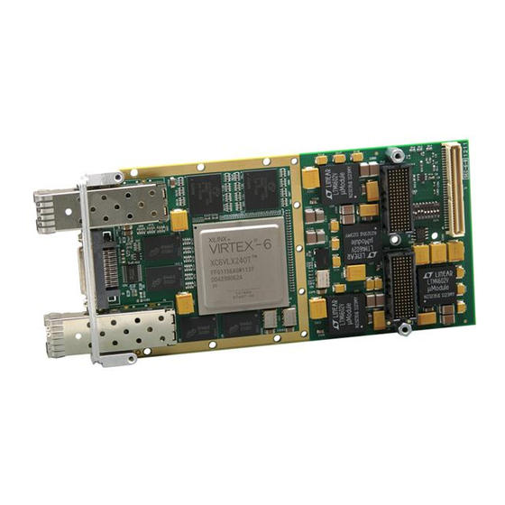
Conduction Cooled Virtex-6 Based FPGA XMC Module
Brand:
Acromag
| Category:
Control Unit
| Size: 3 MB
Table of Contents
Table of Contents
3
1 0 General Information
7
Ordering Information
8
Key Features
8
Pcle Interface Features
9
Software
10
Engineering Design Kit
10
Board Dll Control Software
10
BOARD Vxworks SOFTWARE
10
BOARD Linux SOFTWARE
10
2 0 Preparation for Use
11
Unpacking and Inspecting
11
Card Cage Considerations
11
Heat Sink Considerations
11
Board Installation
11
Default Hardware Configuration
12
P16 Secondary XMC Connector
12
Rear P4 Field I/O Connector
13
Mezzanine Connector
14
Non-Isolation Considerations
15
3 0 Programming Information
16
Getting Started
16
Virtex 6 Configuration
17
Platform Flash Xilinx Configuration
17
BPI Flash Xilinx Configuration
17
Pcie CONFIGURATION ADDRESS SPACE
18
Configuration Registers
18
Bar0 Memory Map
20
Interrupt Controller
21
Interrupt Status Register (Read/Write) - (BAR0 + 0X00100000)
21
Interrupt Pending Register (Read) - (BAR0 + 0X00100004)
22
Interrupt Enable Register (Read/Write) - (BAR0 + 0X00100008)
22
Interrupt Acknowledge Register (Write) - (BAR0 + 0X0010000C)
23
Set Interrupt Enable Register (Write) - (BAR0 + 0X00100010)
23
Clear Interrupt Enable Register (Write) - (BAR0 + 0X00100014)
24
Interrupt Vector Register (Read) - (BAR0 + 0X00100018)
24
Master Enable Register (Read/Write) - (BAR0 + 0X0010001C)
24
Axi-Cdma
25
CDMA Control Register (Read/Write) - (BAR0 + 0X000A0000)
26
CDMA Status Register (Read/Write) - (BAR0 + 0X000A0004)
28
CDMA Current Descriptor Pointer Register (Read/Write) - (BAR0 + 0X000A0008)
31
CDMA Tail Descriptor Pointer Register (Read/Write) - (BAR0 + 0X000A0010)
32
CDMA Source Address Register (Read/Write) - (BAR0 + 0X000A0018)
33
CDMA Destination Address Register (Read/Write) - (BAR0 + 0X000A0020)
33
CDMA Bytes to Transfer Register (Read/Write) - (BAR0 + 0X000A0028)
34
Simple CDMA Programming Example
34
AXI-BAR0 Aperture Base Address
35
Pcie AXI-Bridge Control
36
Physical Side Interface Status/Control Register (Read/Write) - (BAR0 + 0X000F0144)
36
AXI Base Address Translation Configuration Register (Read Only) - (BAR0 + 0Xf0208/0Xf020C)
37
FPGA Fabric MEMORY MAP
38
Front, Rear, and P16 I/O Registers (Read/Write) - (BAR0 + 0X301000 to 0X 301FFF)
39
Front I/O Interrupt Status/Clear Register (Read/Write) - (BAR0 + 0X300000)
39
DDR Memory Test Status Register (Read/Write) - (BAR0 + 0X300008)
40
XMC Board Identification Code Register (Read Only) - (BAR0 + 0X30000C)
40
Configuration Control (Read/Write) - (BAR0 + 0X300100)
40
Aurora Monitor (Read/Write) - (BAR0 + 0X300104)
41
Flash Introduction
41
Flash Status (Read Only) - (BAR0 + 0X300200)
43
Flash Control (Write Only) - (BAR0 + 0X300204)
44
Flash Read (Read Only) - (BAR0 + 0X300208)
44
Flash Start Write (Write Only) - (BAR0 + 0X30020C)
45
Flash Erase Block (Write Only) - (BAR0 + 0X300210)
45
Flash Data Register (Read/Write) - (BAR0 + 0X300214)
45
Flash Address (Read/Write) - (BAR0 + 0X300218)
45
Simple BPI Flash Programming Example
46
Simple Platform Flash Programming Example
46
System Monitor Status/Control Register (Read/Write) - (BAR0 + 0X300300)
47
System Monitor Address Register (Write Only) - (BAR0 + 0X300304)
47
Front Input Data Register (Read Only) - (BAR0 + 0X301000)
48
Front Output Data Register (Read/Write) - (BAR0 + 0X301004)
48
Front I/O Interrupt Enable Register (Read/Write) - (BAR0 + 0X301008)
49
Interrupt Type (COS or H/L) Configuration Register (Read/Write) - (BAR0 + 0X30100C)
49
Interrupt Polarity Register (Read/Write) - (BAR0 + 0X301010)
50
Rear Input Data Register (Read Only) - (BAR0 + 0X301100)
51
Rear Output Data Register (Read/Write) - (BAR0 + 0X301104)
52
P16 Input Data Register (Read Only) - (BAR0 + 0X301200)
53
P16 Output Data Register (Write Only) - (BAR0 + 0X301204)
54
Bar2 Memory Map
55
QDR Memory (Read/Write) - (BAR2 + 0X0000000 to 0X00Ffffff)
55
4 0 Theory of Operation
56
Pci Interface Logic
57
DDR3 Memory
57
QDR II+ SRAM Memory
57
Clock Generation
58
Multi-Gigabit Transceivers (GTX Mgts)
58
SFP Module Connectors
58
USB-To-UART Bridge
58
16MB Platform Flash
59
32MB Linear BPI Flash
59
Configuration Flash Design Considerations
60
JTAG Port
60
DIP Switch
61
Power System Devices
61
System Monitor
63
5 0 XPS Embedded System
64
Xilinx ISE Example Projects
64
Microblaze Peripherals
66
Host Peripherals
67
Common Peripherals
67
Sdk
67
Acromag Peripheral Repository
69
Acromag Modified Library Files
70
Running a Program from BPI FLASH Memory
71
Running LWIP Echo Server
74
EDK File Organization
76
Example EDK Design Modification Walkthrough
76
Service and Repair Assistance
103
Preliminary Service Procedure
103
Where to Get Help
103
6 0 Service and Repair
103
7 0 Specifications
104
Physical
104
Power Requirements
104
Environmental
104
User Programmable (U2) FPGA
105
EDK Example Design
105
P15 Connector
105
P16 Connector
106
P4 Rear I/O
106
Mezzanine Front I/O
106
Board Oscillators
107
DDR3 Memory
107
QDR II+ SRAM Memory
107
16MB Platform Flash
108
32MB Linear BPI Flash
108
Pcie Bus Interface
108
XMC-6VLX Block Diagram
110
Certificate of Volatility
111
Revision History
112
Advertisement
Advertisement
Related Products
Acromag XMC-6280-LF
Acromag XMC-6280 Series
Acromag XMC-6VLX240
Acromag XMC-6VLX365
Acromag XMC-6260-CC
Acromag BusWorks XT1233-000
Acromag BusWorks XT1122-000
Acromag BusWorks XT1121-000
Acromag XVME-6700A
Acromag XVME-6500
Acromag Categories
Control Unit
I/O Systems
Transmitter
Computer Hardware
Carrier boards
More Acromag Manuals
Login
Sign In
OR
Sign in with Facebook
Sign in with Google
Upload manual
Upload from disk
Upload from URL