
Related Manuals for Atmel SAM3S-EK


Summary of Contents for Atmel SAM3S-EK
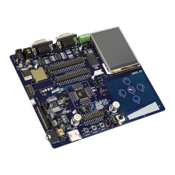
- Page 1 SAM3S-EK Development Board ........................User Guide 11031A–ATARM–14-Dec-09...
-
Page 2: Table Of Contents
4.3.11 USB Device ....................... 4-10 4.3.12 Analog Interface ....................4-11 4.3.13 QTouch Elements ....................4-12 4.3.14 User Buttons ...................... 4-13 4.3.15 LEDs ........................4-13 4.3.16 SD/MMC Card ....................4-14 4.3.17 ZigBEE....................... 4-14 4.3.18 PIO Expansion ....................4-14 SAM3S-EK Development Board User Guide 11031A–ATARM–14-Dec-09... - Page 3 4.5.13 PIO Expansion Port A Connector J13 .............. 4-30 4.5.14 PIO Expansion Port B Connector J14 ............... 4-31 Section 5 Schematics .........................5-1 Schematics......................... 5-1 Section 6 Troubleshooting ......................6-1 Self-Test..........................6-1 Board Recovery ......................... 6-1 Section 7 Revision History......................7-1 Revision History ......................... 7-1 SAM3S-EK Development Board User Guide 11031A–ATARM–14-Dec-09...
-
Page 4: Introduction
SAM3S4C device. User Guide This guide focuses on the SAM3S-EK board as an evaluation platform. It is made up of 6 sections: Section 1 includes references, applicable documents, acronyms and abbreviations. Section 2 describes the kit contents, its main features and specifications. -
Page 5: Kit Contents
– one serial RS232 cable A Welcome Letter Figure 2-1. Unpacked SAM3S-EK Unpack and inspect the kit carefully. Contact your local Atmel distributor, should you have issues con- cerning the contents of the kit. SAM3S-EK Development Board User Guide 11031A–ATARM–14-Dec-09... -
Page 6: Electrostatic Warning
Kit Contents Electrostatic Warning The SAM3S-EK board is shipped in a protective anti-static package. The board must not be subjected to high electrostatic potentials. A grounding strap or similar protective device should be worn when han- dling the board. Avoid touching the components or any other metallic element of the board. -
Page 7: Power Up
The on-board NAND Flash contains “SAM3S-EK DevStart”. It is stored in the “SAM3S-EK DevStart” folder on the USB Flash disk available when the SAM3S-EK is connected to a host computer and you click on the Flash Disk icon of the on-board demo. -
Page 8: Sample Code And Technical Support
A t m e l w e b s i t e http://www.atmel.com/dyn/products/tools_card.asp?tool_id=4678 Figure 3-1. Atmel Website for AT91SAM Products SAM3S-EK Development Board User Guide 11031A–ATARM–14-Dec-09... -
Page 9: Evaluation Kit Hardware
Section 4 Evaluation Kit Hardware Board Overview This section introduces the Atmel SAM3S Evaluation Kit design. It introduces system-level concepts, such as power distribution, memory, and interface assignments. ® ® The SAM3S-EK board is based on the integration of an ARM... -
Page 10: Features List
(IAP) routines. The SAM3S features an External Bus Interface (EBI) that permits interfacing to a broad range of external memories and virtually to any parallel peripheral. The SAM3S-EK board is equipped with a memory device connected to the SAM3 EBI: SAM3S-EK Development Board User Guide 11031A–ATARM–14-Dec-09... -
Page 11: Clock Circuitry
The input frequency of PLLA is from 7.5 and 20 MHz. The SAM3S-EK board is equipped with one 12 MHz crystal, optional Piezoelectric Ceramic Resonator 12 Mhz (Murata ref. CSTCE12M0G15L99-R0), one 32.768 Hz crystal and an external clock input con- nector (optional, not populated by default). -
Page 12: Reset Circuitry
Power Supply and Management The SAM3S-EK board is supplied with an external 5V DC block through input J9. It is protected by a PolyZen diode MN9 and an LC combinatory filter MN10. The PolyZen is used in the event of an incorrect power supply connection. -
Page 13: Uart
2. solder a shunt resistor in place of R25 (a solder drop will do). 4.3.7.1 RS232 SAM3S-EK connects the USART1 bus (including TXD, RXD, RTS, CTS handshake signal controls and EN command) to the DB9 male connector J5 through the RS232 Transceiver MN5. SAM3S-EK Development Board User Guide... -
Page 14: Display Interface
DGND 4.3.8 Display Interface The SAM3S-EK carries a TFT Transmissive LCD module with touch panel, FTM280C34D. Its integrated driver IC is ILI9325. The LCD display area is 2.8 inches diagonally measured, with a native resolution of 240 x 320 dots. - Page 15 The LCD module integrates a 4-wire touch panel controlled by MN7 (ADS7843) which is a slave device on the SAM3S SPI bus. The controller sends back the information about the X and Y positions, as well SAM3S-EK Development Board User Guide 11031A–ATARM–14-Dec-09...
-
Page 16: Jtag/Ice
DGND 4.3.9 JTAG/ICE A standard 20-pin JTAG/ICE connector is implemented on the SAM3S-EK for the connection of a com- patible ARM JTAG emulator interface, such as the SAM-ICE from Segger. Note: The NRST signal is connected to BP1 system button and is also used to reset the LCD mod- ule. -
Page 17: Audio Interface
AGND 4.3.10.2 Headphone Output The SAM3S-EK evaluation kit supports mono/stereo audio playback driven by a TPA0223 audio ampli- fier connected to two DAC channels of the microcontroller. The TPA0223 is a 2W mono Bridge-Tied-Load (BTL) amplifier designed to drive speakers with as low as 4 Ohm impedance. -
Page 18: Usb Device
PIO compatible 3.3V level) through PC21. Figure 4-14. USB USB Micro B USB Micro B FGND V5.5MLA0603 V5.5MLA0603 V5.5MLA0603 V5.5MLA0603 PC21 R110 R110 R112 R112 10pF 10pF DGND FGND DGND PB10 R114 R114 PB11 R116 R116 4-10 SAM3S-EK Development Board User Guide 11031A–ATARM–14-Dec-09... -
Page 19: Analog Interface
50-Ohm resistor termination can be enabled by closing jumper JP21. A filter can be imple- mented on this output channel by replacing R106 and C90 with appropriate resistor and capacitor values, depending on the application requirements. SAM3S-EK Development Board User Guide 4-11 11031A–ATARM–14-Dec-09... -
Page 20: Qtouch Elements
QTouch keys consist in a series of sensors formed by the association of a copper area and the capaci- tive effect of human fingers approaching it. 4.3.13.1 Keys The SAM3S-EK implements five individual capacitive touch keys (UP, DOWN, RIGHT, LEFT and VALID) using five pairs of PIO. Figure 4-18. QST Keys... -
Page 21: User Buttons
22nF 4.3.14 User Buttons There are two mechanical user buttons on the SAM3S-EK, which are connected to PIO lines and defined to be "left" and "right" buttons by default. In addition, a mechanical button controls the system reset, signal NRST. -
Page 22: Sd/Mmc Card
The SAM3S product features three PIO controllers, PIOA, PIOB and PIOC, which are multiplexed with the I/O lines of the embedded peripherals. Each PIO Controller controls up to 32 lines (16 for PIOB). Expansion ports J12, J13 and J14 provide PIO lines access for customer defined usage. 4-14 SAM3S-EK Development Board User Guide 11031A–ATARM–14-Dec-09... - Page 23 PC14 PA14 PA30 PC15 PA15 PA31 +3V3 +3V3 +3V3 +3V3 DGND DGND DGND DGND Note: All PIO lines are available on these expansion connectors, except those that are used for the QTouch elements. SAM3S-EK Development Board User Guide 4-15 11031A–ATARM–14-Dec-09...
-
Page 24: Configuration
Evaluation Kit Hardware Configuration This section describes the PIO usage, the jumpers, the test points and the solder drops of a SAM3S-EK board. 4.4.1 PIO Usage Table 4-1. PIO Port A Pin Assignments and Signal Descriptions Peripheral Peripheral Peripheral System... - Page 25 JTAG test mode select TCK/SWCLK JTAG clock XOUT CLK12MHz CLK12MHz PB10 USB DM PB11 USB DP PB12 PWML1 ERASE Flash erase selector PB13 PWML2 PCK0 DAC0 Audio Output R PB14 NPCS1 PWMH3 DAC1 Audio Output L SAM3S-EK Development Board User Guide 4-17 11031A–ATARM–14-Dec-09...
- Page 26 QTouch down button SNS PC27 TIOB4 QTouch down button SNSK PC28 TCLK4 AD13 QTouch left button SNS PC29 TIOA5 AD14 QTouch left button SNSK PC30 TIOB5 QTouch right button SNS PC31 TCLK5 QTouch right button SNSK 4-18 SAM3S-EK Development Board User Guide 11031A–ATARM–14-Dec-09...
-
Page 27: Jumpers
Evaluation Kit Hardware 4.4.2 Jumpers The SAM3S-EK board jumpers are essentially used for two main purposes: functional selection or cur- rent measurement. Details are given below. Table 4-4. Jumpers Setting Designation Label Default Setting Feature JTAG OPEN Close to select the JTAG boundary scan of the SAM3S Analog reference voltage selection between 3.3V (close 1-2) and... -
Page 28: Test Points
As pointed out in some previous interface description, 0 Ohm resistors have been inserted on the path of the receiver PIO lines of the SAM3S-EK. These are the PIO lines connected to an external driver on the board. The 0 Ohm resistors allow disconnecting each of these for custom usage (through PIO expansion connectors for example). - Page 29 R9, R10 Isolation on 32 KHz clock source and GPIO expansion Optional write protection NAND Flash Optional pull-up for open drain output or equivalent device R24, R30 Differential impedance matching for RS485 cable SAM3S-EK Development Board User Guide 4-21 11031A–ATARM–14-Dec-09...
-
Page 30: Connectors
Connectors 4.5.1 Power Supply Connector J9 The SAM3S-EK evaluation board can be powered from a 5VDC power supply connected to the external power supply jack J9. The positive pole is the center pin. Figure 4-25. Power Supply Connector J9 Table 4-10. Power Supply Connector J9 Signal Descriptions... -
Page 31: Uart Connector J7
GROUND 4.5.4 USB Device Connector J15 Figure 4-27. Micro-B USB Connector J15 Table 4-13. Micro-B USB Connector J15 Signal Descriptions Mnemonic Signal Description Vbus 5v power Data - Data + Ground Shield Shield SAM3S-EK Development Board User Guide 4-23 11031A–ATARM–14-Dec-09... -
Page 32: Tft Lcd Connector J8
LCD_DB05 (NC) LCD_DB04 (NC) LCD_DB03 (NC) LCD_DB02 (NC) LCD_DB01 (NC) LCD_DB00 (NC) RD (PC11) WR (PC8) RS (PC19) CS (PC15) RESET LED-A LED-K1 LED-K2 LED-K3 LED-K4 Y UP Y DOWN X RIGHT X LEFT 4-24 SAM3S-EK Development Board User Guide 11031A–ATARM–14-Dec-09... -
Page 33: Jtag Debugging Connector J6
Connect to RTCK if available, otherwise to GND. Common ground TDO JTAG TEST DATA OUTPUT — JTAG data output from target CPU. Typically connected to TDO on target CPU. Serial data input from the target Common ground SAM3S-EK Development Board User Guide 4-25 11031A–ATARM–14-Dec-09... -
Page 34: Sd/Mmc - Mci Connector J3
This pin is not connected in SAM-ICE. Common ground 4.5.7 SD/MMC - MCI Connector J3 Figure 4-30. SD/MMC Connector J3 Table 4-16. SD/MMC Connector J3 Signal Descriptions Mnemonic Mnemonic RSV/DAT3 DAT0 DAT1 DAT2 Card Detect 4-26 SAM3S-EK Development Board User Guide 11031A–ATARM–14-Dec-09... -
Page 35: Analog Connector Cn1 & Cn2
Figure 4-32. RS485 Connector J14 Table 4-18. RS485 J14 Signal Descriptions Mnemonic A - non-inverted RS485 signal A Frame ground B - non-inverted RS485 signal B 4.5.10 Headphone Connector J11 Figure 4-33. Headphone J11 SAM3S-EK Development Board User Guide 4-27 11031A–ATARM–14-Dec-09... -
Page 36: Zigbee Connector J16
SPI MOSI select SPI MISO MISO SCLK SPI CLK Power Voltage range: 1.8v to 5.5v, typically Supply regulated to 3.3v 4.5.12 PIO Expansion Port C Connector J12 Figure 4-35. PIO Expansion Connector J12 4-28 SAM3S-EK Development Board User Guide 11031A–ATARM–14-Dec-09... - Page 37 PC12 PC13 PC14 PC15 4.5.13 PIO Expansion Port A Connector J13 Figure 4-36. PIO Expansion Connector J13 Table 4-22. Connector J13 Signal Descriptions Mnemonic Mnemonic +5V or +3v3 +5V or +3v3 PA16 PA17 SAM3S-EK Development Board User Guide 4-29 11031A–ATARM–14-Dec-09...
- Page 38 PA31 4.5.14 PIO Expansion Port B Connector J14 Figure 4-37. PIO Expansion Connector J14 Table 4-23. Connector J14 Signal Descriptions Mnemonic Mnemonic +5V or +3v3 +5V or +3v3 PB10 PB11 PB12 PB13 PB14 4-30 SAM3S-EK Development Board User Guide 11031A–ATARM–14-Dec-09...
- Page 39 Evaluation Kit Hardware Table 4-23. Connector J14 Signal Descriptions Mnemonic Mnemonic SAM3S-EK Development Board User Guide 4-31 11031A–ATARM–14-Dec-09...
- Page 40 Section 5 Schematics Schematics This section contains the following schematics: Block diagram General information Microcontroller NAND Flash, serial interface TFT LCD & Touch Audio & Power Supply USB, LEDs, push-buttons & ZigBEE SAM3S-EK Development Board User Guide 11031A–ATARM–14-Dec-09...
- Page 41 SAM3S-EK RevB Block Diagram ATMEL Cortex M3 Processor SAM3S (LQFP100) Reset,Debug Logic Power Manage 2.8 Inch TFT-LCD Audio PA Microphone MicroSD Card USB FS Device Nand Flash RS232 & RS485 QTouch Input AD/DA ZIGBEE IF User Interface (PIO PortA,B,C) 26-NOV-09...
-
Page 42: Revision History
MODIF. MODIF. MODIF. DES. DES. DES. DATE DATE DATE VER. VER. VER. DATE DATE DATE SAM3S-EK SAM3S-EK SAM3S-EK SCALE SCALE SCALE REV. REV. REV. SHEET SHEET SHEET Describe Describe Describe This agreement is our property. Reproduction and publication without our written authorization shall expose offender to legal proceedings. - Page 43 XX-XXX-XX DGND MODIF. MODIF. MODIF. DES. DES. DES. DATE DATE DATE VER. VER. VER. DATE DATE DATE SAM3S-EK SAM3S-EK SAM3S-EK SCALE SCALE SCALE REV. REV. REV. SHEET SHEET SHEET VDDCORE VDDIO Microcontroller Microcontroller Microcontroller This agreement is our property. Reproduction and publication without our written authorization shall expose offender to legal proceedings.
- Page 44 XX-XXX-XX MODIF. MODIF. MODIF. DES. DES. DES. DATE DATE DATE VER. VER. VER. DATE DATE DATE SAM3S-EK SAM3S-EK SAM3S-EK SCALE SCALE SCALE REV. REV. REV. SHEET SHEET SHEET FGND NAND FLASH,SERIAL INTERFACE NAND FLASH,SERIAL INTERFACE NAND FLASH,SERIAL INTERFACE This agreement is our property. Reproduction and publication without our written authorization shall expose offender to legal proceedings.
- Page 45 MODIF. MODIF. MODIF. DES. DES. DES. DATE DATE DATE VER. VER. VER. DATE DATE DATE SAM3S-EK SAM3S-EK SAM3S-EK SCALE SCALE SCALE REV. REV. REV. SHEET SHEET SHEET TFT-LCD & QTouch TFT-LCD & QTouch TFT-LCD & QTouch This agreement is our property. Reproduction and publication without our written authorization shall expose offender to legal proceedings.
- Page 46 MODIF. MODIF. MODIF. DES. DES. DES. DATE DATE DATE VER. VER. VER. DATE DATE DATE SAM3S-EK SAM3S-EK SAM3S-EK SCALE SCALE SCALE REV. REV. REV. SHEET SHEET SHEET Audio & Power Supply Audio & Power Supply Audio & Power Supply This agreement is our property. Reproduction and publication without our written authorization shall expose offender to legal proceedings.
- Page 47 MODIF. MODIF. MODIF. DES. DES. DES. DATE DATE DATE VER. VER. VER. DATE DATE DATE SAM3S-EK SAM3S-EK SAM3S-EK SCALE SCALE SCALE REV. REV. REV. SHEET SHEET SHEET MISC MISC MISC This agreement is our property. Reproduction and publication without our written authorization shall expose offender to legal proceedings.
-
Page 48: Troubleshooting
Closing JP3 and powering the board will assert ERASE and clear GPNVM bit 1, and thereby selects the boot from the ROM by default. The MCU will boot from the internal ROM to enable a SAM-BA connection through the UART. Connect the SAM3S-EK UART port (J3) to a PC COM port through an RS232 cross- over cable. - Page 49 Section 7 Revision History Revision History Table 7-1. Change Request Document Comments Ref. 11031A First issue. SAM3S-EK Development Board User Guide 11031A–ATARM–14-Dec-09...
- Page 50 Disclaimer: The information in this document is provided in connection with Atmel products. No license, express or implied, by estoppel or otherwise, to any intellectual property right is granted by this document or in connection with the sale of Atmel products. EXCEPT AS SET FORTH IN ATMEL’S TERMS AND CONDI- TIONS OF SALE LOCATED ON ATMEL’S WEB SITE, ATMEL ASSUMES NO LIABILITY WHATSOEVER AND DISCLAIMS ANY EXPRESS, IMPLIED OR STATUTORY...
Need help?
Do you have a question about the SAM3S-EK and is the answer not in the manual?
Questions and answers