Table of Contents
Advertisement
Quick Links
Advertisement
Table of Contents

Related Manuals for Microsemi IGLOO PLUS Starter Kit


Summary of Contents for Microsemi IGLOO PLUS Starter Kit
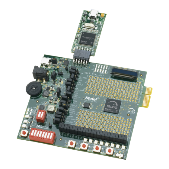
- Page 1 IGLOO PLUS Starter Kit User’s Guide...
-
Page 3: Table Of Contents
Getting Started with the IGLOO PLUS Starter Kit Demo Design ....... - Page 4 Table of Contents C Product Support ..............59 Customer Service .
-
Page 5: Introduction
IGLOO PLUS devices. Table 1 lists the contents of the box. Table 1 • IGLOO PLUS Starter Kit Contents Quantity Contents IGLOO PLUS board with AGLP125 IGLOO PLUS field programmable gate array (FPGA) Programmer for use with IGLOO PLUS board 5 V power supply USB 2.0 high-speed cables... -
Page 7: Board Components And Settings
This chapter describes the components and settings for the IGLOO PLUS Starter Kit Board. Board Description The IGLOO PLUS Starter Kit board is intended to provide a low-cost system platform for evaluating IGLOO PLUS (AGLP) technology, such as low power, I/O state preservation during Flash*Freeze mode, and Schmitt Triggered I/Os. -
Page 8: Igloo Plus Board Stackup
Figure 1-1 Figure 1-1 on page 7 show the top (L1) and bottom (L10) silkscreens. The full PCB design layout is provided on the Microsemi SoC Products Group website, on the IGLOO PLUS Starter Kit page: www.microsemi.com/soc/products/hardware/devkits_boards/iglooplus_starter.aspx. To view the PCB... - Page 9 IGLOO PLUS Starter Kit User’s Guide Figure 1-2 • IGLOO PLUS Top Silkscreen (L1) R e v i s i o n 1...
- Page 10 Board Components and Settings Figure 1-3 • IGLOO PLUS Bottom Silkscreen (L10) R e visio n 1...
-
Page 11: Connectors, Jumpers, And Switch Settings
IGLOO PLUS Starter Kit User’s Guide Connectors, Jumpers, and Switch Settings Recommended default jumper settings are defined in Table 1-1. The voltage selection jumpers are highlighted in grey. Connect jumpers in the default settings described in Table 1-1 to enable the pre- programmed demo design to function correctly. - Page 12 Board Components and Settings Table 1-1 • Jumper and Connector Settings (continued) Jumper Default Setting Comment Pin 2-4 Select 3.3 V, 1.5 / 1.2 V, or 2.5 V for VCCI_0 Pin 2-4 = 3.3 V Pin 3-4 = 1.5 V or 1.2 V Pin 1-4 = 2.5 V Pin 2-3 Current measurement header for VJTAG...
- Page 13 IGLOO PLUS Starter Kit User’s Guide Table 1-2 • Switch Settings Switch Default Setting Comment SW1–SW4 Push-button switches for SWITCH[1:4] CLOSE Contains DIP switches for 3V3_SWITCH[1:2] DSW5 CLOSE Contains DIP switches for D_SWITCH[1:8] Push-button switch for system reset PBRESET_N Flash*Freeze: To enable Flash*Freeze mode, SW8 toward ON.
-
Page 15: Fpga Description
RAM kbits (1,024 bits) 4,608-Bit Blocks FlashROM (bits) Secure (AES) ISP Integrated PLLs in CCCs VersaNet Globals I/O Banks Maximum User I/Os For further information, refer to the IGLOO PLUS datasheet: www.microsemi.com/soc/documents/IGLOOPLUS_DS.pdf R e v i s i o n 1... -
Page 16: Power And Ground Pins
FPGA Description Power and Ground Pins Figure 2-1 shows the power and ground pins for AGLP125-CSG289. AGLP125 CSG289 SEC 5/6 SEC 5/6 VCOMPLF GND1 GND2 VCCPLF VCCPLF GND3 GND4 GND5 VCC1 GND6 GND7 VCC2 GND8 GND9 VCC3 GND10 GND11 VCC4 GND12 GND13 GND14... - Page 17 IGLOO PLUS Starter Kit User’s Guide Bank I/O Signals Figure 2-2 through Figure 2-5 on page 19 show the schematics for the bank I/O signals. AGLP125 CSG289 SEC 1/6 SEC 1/6 GPIOA_1 {3} TP105 TP105 AGL_B0_PIN_B3 TP96 TP96 IO06RSB0 IO38RSB0...
- Page 18 FPGA Description AGLP125 CSG289 SEC 2/6 SEC 2/6 GPIOA_2 TP38 TP38 AGL_B1_PIN_E14 TP39 TP39 IO64RSB1 GBA2/IO63RSB1 GPIOA_4 TP45 TP45 AGL_B1_PIN_E15 TP104 TP104 IO66RSB1 GBB2/IO65RSB1 GPIOA_6 TP44 TP44 AGL_B1_PIN_F13 TP42 TP42 IO68RSB1 GBC2/IO67RSB1 GPIOA_8 TP40 TP40 AGL_B1_PIN_H14 TP226 TP226 IO69RSB1 GCA0/IO84RSB1 GPIOA_10 TP26 TP26...
- Page 19 IGLOO PLUS Starter Kit User’s Guide AGLP125 CSG289 SEC 4/6 SEC 4/6 AGL_B3_PIN_P2 AGL_B3_PIN_E4 TP235 TP235 IO171RSB3 GAA2/IO211RSB3 AGL_B3_PIN_M4 AGL_B3_PIN_F5 TP203 TP203 IO172RSB3 GAB2/IO209RSB3 AGL_B3_PIN_L5 AGL_B3_PIN_E3 TP218 TP218 IO173RSB3 GAC2/IO207RSB3 AGL_B3_PIN_P1 AGL_B3_PIN_N4 TP245 TP245 IO174RSB3 GEA0/IO165RSB3 AGL_B3_PIN_K5 AGL_B3_PIN_T1 TP227 TP227...
-
Page 20: Jtag Pins
FPGA Description JTAG Pins The AGLP125-CSG289 has advanced I/O features such as JTAG pins for IEEE 1149.1 JTAG Boundary Scan Test. These pins are utilized during programming of the FPGA (Figure 2-6). Low-power flash devices have a separate bank for these dedicated JTAG pins. The JTAG pins can be run at any voltage from 1.5 V to 3.3 V (nominal). -
Page 21: Decaps And Ground Post Schematics
IGLOO PLUS Starter Kit User’s Guide Decaps and Ground Post Schematics The schematics for the decaps and ground post are shown in Figure 2-7. DECAPS FOR VCORE VCORE DECAPS FOR I/O BANK0 , BANK1 ,BANK2 & BANK3 VCCI_0 VCCI_1 VCCI_2... -
Page 23: Power
3 – Power The IGLOO PLUS development board is powered through an external voltage power brick or USB. The board does not switch seamlessly between the power brick and USB, so the 4-pin header and jumper must be used to select the desired power source. In the USB option, the in-rush current meets the USB specifications (see Figure 3-1). -
Page 24: Power Modes
Power Power Modes In addition to the board, the IGLOO PLUS FPGA offers power advantages. Some key power advantages of the IGLOO PLUS FPGAs are as follows: • Flash*Freeze technology enables easy entry and exit from the static Low-power mode, where IGLOO consumes as little as 5 µW while retaining the contents of the system memory and data registers. -
Page 25: Battery
IGLOO PLUS Starter Kit User’s Guide Battery In addition to the power brick and USB, this board provides the option to power-up via battery. No battery casing is provided on the board. Jumpers should be set correctly to select the option of either powering through a wall/USB or through batteries hooked up externally. -
Page 26: Current Measurement
Power 1V5_1V2 VCC_SWEEP 5K pot 5K pot Figure 3-4 • Schematic for Potentiometer Current Measurement Once the IGLOO PLUS evaluation board is powered up, you can evaluate power consumption using the current measurement four-pin headers on the board (Figure 3-5). Current measurement can be made without powering down the board. - Page 27 IGLOO PLUS Starter Kit User’s Guide Current Measurement IGLOO PLUS 3.3 V VCCI_0 VCCI_1 3.3 V VCCI_2 3.3 V or 2.5 V VCCI_3 3.3 V or 2.5 V 1.5 V 3.3 V JTAG 3.3 V PUMP Figure 3-6 • Current Measurement Headers for Power Rails...
-
Page 29: Operation Of Board Components
FPGA to provide a system or reference clock. The PLL can be configured and instantiated in the FPGA to generate a wide range of clock frequencies. Reference For more information, refer to the IGLOO PLUS Starter Kit website page: www.microsemi.com/soc/products/hardware/devkits_boards/iglooplus_starter.aspx. Schematic Figure 4-1 shows the schematic for the clock oscillator. -
Page 30: Flash*Freeze Mode
IP can be used in type 2 mode for clock and data management while entering and exiting Flash*Freeze mode. For more information and detailed usage of Flash*Freeze modes, refer to the “Microsemi’s Flash*Freeze Technology and Low Power Modes” chapter of the IGLOO PLUS FPGA Fabric User’s... - Page 31 IGLOO PLUS Starter Kit User’s Guide Flash*Freeze Types Type 1: Controlled by dedicated Flash*Freeze Pin. Type 2: Controlled by dedicated Flash*Freeze Pin and Internal Logic. Flash*Freeze Type 1: Controlled by Dedicated Flash*Freeze Pin Flash*Freeze type 1 is intended for systems where either the device is reset upon exiting Flash*Freeze mode, or data and clock are managed externally.
- Page 32 Flash*Freeze mode, such as transitioning into a safe state, completing the processing of a critical event. Designers are encouraged to take advantage of the Flash*Freeze Management IP of Microsemi to handle clean entry and exit of Flash*Freeze mode. The device will only enter Flash*Freeze mode when the Flash*Freeze pin is asserted (active low) and the User Low Static ICC (ULSICC) macro input signal, called the LSICC signal, is asserted (high).
- Page 33 IGLOO PLUS Starter Kit User’s Guide Normal Normal Flash*Freeze Operation Operation Mode Flash*Freeze Pin LSICC Signal t = 1 µs t = 1 µs Figure 4-7 • Flash*Freeze Mode Type 1 and Type 2 – Signal Assertion and Deassertion Values Table 4-1 •...
- Page 34 Operation of Board Components Table 4-2 shows the I/O pad state based on the configuration and buffer type. Table 4-2 • IGLOO PLUS Flash*Freeze Mode (type 1 and type 2)—I/O Pad State I/O Pad I/O Pad State in Flash*Freeze Buffer Type Hold State Weak Pull-Up/-Down Mode...
- Page 35 IGLOO PLUS Starter Kit User’s Guide Flash*Freeze Switch An F*F switch is provided on the board for designs that utilize the Flash*Freeze technology. Setting the F*F switch to FF_ON will enable the Flash*Freeze mode of the IGLOO PLUS device. Since the Schmitt...
- Page 36 Operation of Board Components Flash*Freeze Variant FET LEDs These FET LEDs can be used for debugging, such as for viewing the state of I/Os in Flash*Freeze mode. These LEDs can be activated (ON) before entering Flash*Freeze mode, and have the ability to remain activated (ON) in Flash*Freeze mode.
-
Page 37: Push-Button Switches
IGLOO PLUS Starter Kit User’s Guide Push-Button Switches Four active low push-button switches are provided on the board for debug purposes. You can remove the corresponding jumpers to detach or isolate any of the four push-button test switches from the FPGA I/O. -
Page 38: Dip Switches
Operation of Board Components .DIP Switches A DIP switch pack (8 switches) is provided on the board (Figure 4-13 Figure 4-14). You can remove the corresponding jumpers to detach or isolate any of the eight DIP Switches from the FPGA I/Os.. DSW5 DSW5 D_SWITCH1 [4]... -
Page 39: User Leds
IGLOO PLUS Starter Kit User’s Guide User LEDs Eight active low debug LEDs are provided on the board (Figure 4-15 Figure 4-16). You can remove the corresponding jumpers from the 8 × 2 headers to detach or isolate any of the eight LEDs from the FPGA I/Os. -
Page 40: I/O Test Pins
Operation of Board Components I/O Test Pins All IGLOO PLUS FPGA I/Os are available on headers located on the top and bottom of the device (Figure 4-17 Figure 4-18). These test pins are multiples of 100 mils apart, so developers can easily attach headers and place an extension card on top with an off-the-shelf breadboard for a low-cost solution for integration. -
Page 41: Oled
The demo design included in this kit contains a roulette game that uses the OLED for display and the push-button switch for game control. Additional OLED info is available at the IGLOO PLUS Starter Kit website page: www.microsemi.com/soc/products/hardware/devkits_boards/iglooplus_starter.aspx. -
Page 42: Interface Connector
PLUS FPGA. Any standard UART controller can be implemented in the IGLOO PLUS FPGA to allow access with this interface. In addition, the Microsemi IP catalog includes various UART controllers, specifically CoreUART, which can be instantiated in the FPGA design with an embedded processor. -
Page 43: Spi Flash
I2C. In the schematics shown in Figure 4-22, either the Winbond or Atmel 2 Mbyte SPI flash will be populated on-board. Winbond and Atmel SPI flash datasheets are available at the IGLOO PLUS Starter Kit website page: www.microsemi.com/soc/products/hardware/devkits_boards/iglooplus_starter.aspx 2 MByte SPI FLASH... -
Page 44: Low-Cost Programming Stick (Lcps)
Figure 4-23 • Low-Cost Programming Stick (LCPS) Note: 1. The LCPS supplied with this kit is intended for use with the IGLOO PLUS Starter Kit. An LCPS supplied for other kits, although electrically and functionally equivalent, may not connect seamlessly with the IGLOO PLUS Starter Kit board. - Page 45 IGLOO PLUS Starter Kit User’s Guide Programmer VJTAGENB VJTAGENB GND3 GND2 VJTAG TRST VJTAG TRSTB VPUMP VPUMP GND4 GND5 HEADER 6x2/SM HEADER 6x2/SM 6X2 Right Angled Header Mfr P/N :TSW-106-08-T-D-RA Mfr: SAMTEC Figure 4-24 • FPGA Programming Headers Schematic R e v i s i o n 1...
- Page 46 Operation of Board Components LCPS Stackup The LCPS is built on a four-layer PCB with the layers arranged in the following stackup: 1. Top signal layer (Figure 4-25) 2. Ground plane 3. Power plane 1. Bottom signal layer (Figure 4-26 on page Figure 4-25 •...
- Page 47 IGLOO PLUS Starter Kit User’s Guide Figure 4-26 • Low-Cost Programming Stick – Bottom Silkscreen R e v i s i o n 1...
-
Page 49: Programming
4. When using the FlashPro software, the programmer to select is the FlashPro3. The LCPS is functionally equivalent to a FlashPro programmer but designed specifically for use with the IGLOO PLUS Starter Kit. 5. Alternatively, an option (10-pin FP3 header) is provided to program the FPGA with a FlashPro3... -
Page 51: Igloo Plus Board Demo
1. Before starting Demo 1, check the jumper settings and set all switches to the OFF or CLOSE position. Ensure the F*F switch is in the OFF position. 2. Power-on the IGLOO PLUS Starter Kit board using the power supply or USB cable included in the starter kit. - Page 52 IGLOO PLUS Board Demo Table 6-1 • LED[8:1] (continued) Description LED D6 Binary Counter[2] LED D7 Binary Counter[1] LED D8 Binary Counter[0] Demo 2 – OLED Interface Demonstration This demo includes a simple Roulette game provided by Avnet Memec that demonstrates control and operation of the OLED display.
- Page 53 1. Similar to Demo 1, before starting Demo 4, check the jumper settings and set all switches to the OFF or CLOSED position. Ensure the F*F switch is in the OFF position. 2. Power-on the IGLOO PLUS Starter Kit board using the power supply or USB cable included in the starter kit.
- Page 54 IGLOO PLUS Board Demo The FET Truth Table (Table 6-4) shows the Flash*Freeze variants based on the FET I/O HOLD and resister pull configured for this demo design. For the output FET LEDs, NORMAL represents the LED state before entering and after exiting Flash*Freeze mode, while F*F Mode represents the LED state during Flash*Freeze mode.
-
Page 55: A Resources
A – Resources IGLOO PLUS Starter Kit www.microsemi.com/soc/products/hardware/devkits_boards/iglooplus_starter.aspx IGLOO PLUS Overview www.microsemi.com/soc/products/iglooplus/default.aspx IGLOO PLUS Datasheet www.microsemi.com/soc/documents/IGLOOPLUS_DS.pdf IGLOO PLUS FPGA Fabric User’s Guide www.microsemi.com/soc/documents/IGLOOPLUS_UG.pdf Libero IDE Design Software www.microsemi.com/soc/products/software/libero/default.aspx R e v i s i o n 1... -
Page 57: B List Of Changes
B – List of Changes The following table lists critical changes that were made in the current version of the chapter. Date Changes Page Added note in "Low-Cost Programming Stick (LCPS)" section. (SAR 22976) Revision 1 (February, 2013) Note: *The part number is located on the last page of the document. The digits following the slash indicate the month and year of publication. -
Page 59: C Product Support
Microsemi SoC Products Group staffs its Customer Technical Support Center with highly skilled engineers who can help answer your hardware, software, and design questions about Microsemi SoC Products. The Customer Technical Support Center spends a great deal of time creating application notes, answers to common design cycle questions, documentation of known issues, and various FAQs. -
Page 60: Itar Technical Support
For technical support on RH and RT FPGAs that are regulated by International Traffic in Arms Regulations (ITAR), contact us via soc_tech_itar@microsemi.com. Alternatively, within Cases, select Yes in the ITAR drop-down list. For a complete list of ITAR-regulated Microsemi FPGAs, visit the ITAR web page. -
Page 61: Index
7 stackup 8 board stackup –?? product support customer service 59 email 59 contacting Microsemi SoC Products Group My Cases 60 customer service 59 outside the U.S. 60 email 59 technical support 59 web-based technical support 59 website 59... - Page 62 Microsemi Corporate Headquarters One Enterprise, Aliso Viejo CA 92656 USA © 2013 Microsemi Corporation. All rights reserved. Microsemi and the Microsemi logo are trademarks of Within the USA: +1 (949) 380-6100 Microsemi Corporation. All other trademarks and service marks are the property of their respective owners.
- Page 63 Authorized Distribution Brand: Website: Welcome to visit www.ameya360.com Contact Us: Address: 401 Building No.5, JiuGe Business Center, Lane 2301, Yishan Rd Minhang District, Shanghai , China Sales: Direct +86 (21) 6401-6692 Email amall@ameya360.com 800077892 Skype ameyasales1 ameyasales2 Customer Service: Email service@ameya360.com Partnership:...
Need help?
Do you have a question about the IGLOO PLUS Starter Kit and is the answer not in the manual?
Questions and answers