Advertisement
Quick Links
LX7720 Daughter Board User's Manual
Introduction
The
LX7720
provides four half-bridge drivers with floating current sense for motor coil driving, six bi-level inputs for
position sensing, and a resolver to digital interface with primary coil driver. The LX7720 supports a ground potential
difference between the motor and signal grounds of up to 10V and motor supply voltages up to 60V.
When used with an FPGA or MCU controller, the LX7720 provides a complete open- or closed-loop motor driver with coil
current feedback and rotation or linear position sensing for stepper motors, brushless DC and permanent magnet motors.
Position sensing supports encoders, hall sensors, resolvers, synchros, and LVDTs. Resolver carrier frequencies from
360Hz to 20kHz are supported. FPGA IP modules are available to support motor driving functions from open loop cardinal
step driving to space vector modulation using field oriented control.
The LX7720 contains 7 sigma delta modulators for analog acquisition. Sinc filtering and decimation is performed in the
FPGA or MCU controller. Four modulators sample the voltage across floating current sense inputs. The remaining three
modulators sample differential analog inputs such as the filtered drive waveform and output waveforms of a resolver.
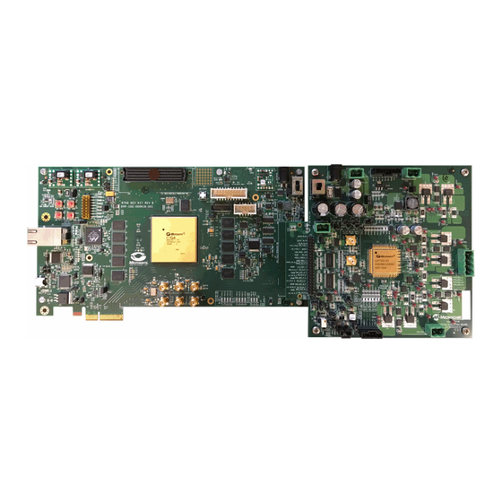
The LX7720 daughter board uses an FMC connector for plug-in connection to the
PolarFire
FPGA
MPF300-EVAL-KIT
signals for connection to other boards such as the
MCU
Evaluation Kit
(Figure 4 on page 2), and the
Kit Contents
•
LX7720 evaluation board SOL-12-000003-11 with soldered-in-place LX7720-ES engineering sample
•
Engineering sample (-ES marking suffix) explanation sheet
•
24V 1.5A universal input AC adapter
•
20x 0.1" pitch shorting jumpers
•
4x 2-position 5mm pitch terminal block sockets, EB9A-02-C or equivalent to mate J12, J18, J30, and J31
•
4-position 5mm pitch terminal block sockets, OSTTJ047150 or equivalent, to mate J9
•
3-position Molex 50-57-9403 2.54mm pitch wire housing latching header to mate J13
•
6-position Molex 50-57-9406 2.54mm pitch wire housing latching header to mate J14
•
8-position Molex 50-57-9408 2.54mm pitch wire housing latching header to mate J15
•
20x Molex 16-02-0096 crimp sockets to suit 24 - 30AWG wire, for J13, J14, and J15 housings
•
USB stick with documentation (see section 1 on page 3)
Figure 1. LX7720 Daughter Board Connected to
June 2020
© 2020 Microsemi Corporation
LX7720 Daughter Board User's Manual
(Figure 2 on page 2) development boards. A 40-way header provides the same
ProASIC3
FPGA
SAMV71Q21RT
RTG4 DEV-KIT
LX7720 Daughter Board rev 2.1
RTG4
FPGA
Starter Kit
(Figure 3 on page 2), the
MCU
SAM V71 Xplained evaluation
using the FMC Connector
Production Datasheet
DEV-KIT
(Figure 1) and
SAMRH71F20
kit.
1
Advertisement

Related Manuals for Microsemi LX7720


Summary of Contents for Microsemi LX7720
- Page 1 10V and motor supply voltages up to 60V. When used with an FPGA or MCU controller, the LX7720 provides a complete open- or closed-loop motor driver with coil current feedback and rotation or linear position sensing for stepper motors, brushless DC and permanent magnet motors.
- Page 2 LX7720 Daughter Board User's Manual Figure 2. PolarFire MPF300-EVAL-KIT Evaluation Kit Board with 300K LE PolarFire FPGA in an FCG1152 Package Figure 3. ProASIC3E Starter Kit with A3PE1500-PQ208 FPGA Contact factory to obtain a flexible circuit to connect a SAMRH71F20-EK...
-
Page 3: Documentation And Support
• Check that the power slide switch on the LX7720 board is off (top/up position) • Power the RTG4 board with its 12V output AC adaptor, and the LX7720 board with its 24V output AC adaptor (Figure 5 below) •... -
Page 4: Using The Gui
LX7720 Daughter Board User's Manual Program RTG4 Firmware Run Flashpro to program RTG4 using one of the following binaries as appropriate: • For BLDC with resolver, use Top_RS.stp in RTG4 Programming Binaries\BLDC motor Resolver directory • For sensorless BLDC, use Top_SL.stp in RTG4 Programming Binaries\BLDC motor Sensorless directory Using the GUI •... - Page 5 LX7720 Daughter Board to RTG4 Development Kit Setup Example • Use the Configure Motor Specification button to change the motor specifications • The GUI automatically plots waveforms when motor starts running • The block diagram below shows the input and output parameters •...
- Page 6 Board Sockets and Link Configuration Figure 6 below identifies major circuit blocks, LEDs, and connectors. Figure 7 on page 7 identifies link headers that configure signal and power supply options on the board, and set LX7720 pin configurations. Table 1 on page 7 summarizes the functions of all connectors and link headers, and provides clickable links to the appropriate parts of section 4 starting on page 10, which provides more detail and schematic around each one.
- Page 7 Select shorter DMOD_OUT_N pin 44 and DMOD_OUT_P pin 46 driver page 16 propagation Pin 1 to VDD propagation delay by setting LX7720 DMOD_BW pin 114 = high. Nearby VDD delay points include J38 pin 1 and J40 pin 1 June 2020 LX7720 Daughter Board rev 2.1...
- Page 8 PWM Couple the filtered resolver/LVDT driver outputs LX7720 DMOD_OUT_N pin 44 Resolver/LVDT Link 1 to 2 and DMOD_OUT_P pin 46 to LX7720 ADC3_N pin 36 and ADC3_P pin 37 for 4.13, driver page 16 measurement of the drive amplitude and fault detection...
- Page 9 4.10, page LX7720 RESET pin 18 is controlled by an external signal on FMC connector J10 Managed by pin G16 or 40 pin header J20 pin 31. A pull-down resistor ensures that LX7720 controller on Link 2 to 3 remains out of reset condition if the external signal is open...
- Page 10 J18 (Table 3, Figure 10). While the LX7720 allows a logic supply range of 2.1V to 5.5V, the LX7720 daughter board's allowed range is 2.7V to 3.6V. This limitation is due to the supply range of the ASVMPC-27.000MHZ-LR-T 27MHz oscillator module Y2, and the SN74LVTH16245A bus transceivers that interface both the 2x20 pin controller interface header J20 and the RTG4 interface FMC connector J10.
- Page 11 LX7720 Daughter Board Configuration Options VDD_3P3V_FMC VDD_3P3V_FMC 12P0V_FMC VDD_R 12V/15V_VIN_U4 R101 C104 C105 R102 0/0805 C118 C119 20k/1%/0805 HDR_3_100MIL HDR_3_100MIL 1uF/25V/0805 0.1uF/25V/0805 0.1uF/25V/0805 4.7uF/10V/0805 REG103GA-A R103 13k/1%/0805 VDD_3P3V VDD_3P3V HDR_2_100MIL C106 C107 0.1uF/25V/0805 4.7uF/10V/0805 LTST-C190GKT OSTOQ027150 GREEN,10mA R105 150R/0805 Figure 10. VDD Logic Supply (3.3V) Regulator Schematic VCC Signal Supply (5V) Regulator Settings The headers J35 and J17 select either the on-board 5V regulator and its power source, or an external 4.5V to 5.5V power...
- Page 12 LX7720 Daughter Board User's Manual VEE Negative Supply Settings The header J3 selects either the LX7720's internal VEE charge pump, or an external -8V to -VGS power supply connected to J4 (Table 5, Figure 12). Table 5. VEE Negative Supply Link Settings...
- Page 13 Charge Pump CP_CLK Selection There are 4 possible sources for the 100kHz to 300kHz charge pump clock, CP_CLK_D at LX7720 pin 13. The 2x20 pin controller interface header J20 and RTG4 Interface FMC connector J10 are wired in parallel to deliver an external clock CP_CLK_C, which is buffered by a gate in U12 (SN74LVTH16245A) to become CP_CLK.
- Page 14 Link 2 to 1 Reset clears latched OC_FAULT, PR_FAULT, and/or over-temperature shutdown faults LX7720 RESET pin 18 is controlled by an external signal on FMC connector J10 pin G16 (RTG4 board) or 40 pin header J20 pin 31 (other controller).
- Page 15 Bi-Level Comparator Inputs BL1 to BL6 The LX7720's 6 bi-level comparator inputs BLI1 to BLI6 are routed to connector J15 pins 3 to 8 respectively. The common comparator threshold LX7720 BLI_TH pin 119 is set to VCC/2 by R4 & R5.
- Page 16 Links J5 to J8 configure the resolver/LVDT driver outputs with or without LC filtering for primary drive wave shaping. Link J5 is left open by default to set LX7720 DMOD_BW pin 114 = low, selecting the longer DMOD_OUT_N pin 44 and DMOD_OUT_P pin 46 driver propagation delay.
-
Page 17: Motor Connections
Bi-Level Detector output 1 MSIO249NB6 GPIO21NB2 SCP input via J38 link header MSIO282NB5 GPIO176NB4 Table 14. Mapping of HPC1-FMC pins, LX7720 pins, and RTG4 and PolarFire FPGA pins on the EVBs June 2020 LX7720 Daughter Board rev 2.1 © 2020 Microsemi Corporation... - Page 18 17 on page 19 Other inputs and outputs are VDD logic level signals directly to and from LX7720 pins, and these signals are highlighted in red, unless the description shows the signal passing through a link header. These signals are highlighted in green. See Table 1 on page 7 for link header configuration details.
- Page 19 Control and Acquisition Signals Headers J10 and J20 Table 16. LX7720 Control and Acquisition Signals HPC1-FMC Connector J10 Pinout (F to K) Signal Signal Signal Signal Signal UD_IN_C_C CLK_OUT_C LD_IN_B_C MOD_CLK_C ADC3_C ADC2_C LD_IN_A_C SNS_OUT_A_C SNS_OUT_D_C SNS_OUT_B_C SNS_OUT_C_C RESET SM_EN...
-
Page 20: Complete Schematics
LX7720 Daughter Board User's Manual Complete Schematics 10-18V @ 1A 5V @ 200mA VCC_1 VCC_2 0.1uF/50V/0805 10uF/50V/0805 10uF/50V/0805 220uF/50V 220uF/50V 10uF/50V/0805 0.1uF/50V/0805 MGND_6 SGND_6 MGND_7 5V @ 200mA 2.3-2. 7V EXT_VREF VREF_IN DMOD_PS VOUT VREF_IN R1 0R/0805 HDR_3_100MIL 0.1uF/50V/0805 10uF/50V/0805 0.1uF/50V/0805... - Page 21 BLO4 HDR_3_100MIL J_RESET BLO5 MOD_CLK_D R136 33R / DNL BLO5 BLO5 BLO6 R143 BLO6 BLO6 MOD_CLK R156 R140 R141 100K/0805 49.9/1%/0805 49.9/1%/0805 LX7720 Figure 23. FPGA and Sensor Connection June 2020 LX7720 Daughter Board rev 2.1 © 2020 Microsemi Corporation...
- Page 22 LX7720 Daughter Board User's Manual VMPS VMPS 0.1uF/250V/1206 0.1uF/250V/1206 STPS 5H100SF STPS5H100SF TP 52 VFLT_C VFLT_C TP20 1N4148WS VFLT_A VFLT_A IRFS31N20DPBF / IRFR3410 TP 53 IRFS31N20DPBF / IRFR3410 1N4148WS UD_C UD_C TP21 1uF/50V/1206 1uF/50V/0805/DNL UD_A 20R/1W/2512 PDS4200H-13 UD_A 1uF/50V/1206 1uF/50V/0805/DNL...
- Page 23 FUSE 6. 3A 350V RADIAL VMPS_IN CDBZ310200H-HF 350VAC/140VDC/ 6.3A FUSE 100K/0805 VM PS STN3NF06 VMPS 56200001009 STMicroelectronics STN3NF06 FUSE_HLD_THT 2.7K/0805 STN3NF06 22uF/100V 22uF/100V 220uF/100V OSTOQ027150 Figure 26. Power Section June 2020 LX7720 Daughter Board rev 2.1 © 2020 Microsemi Corporation...
- Page 24 LX7720 Daughter Board User's Manual GND1 RES1 GND41 PG_C2M GND74 DP1_M2C_P GND21 DP0_C2M_P GND61 HA01_P_CC DP1_M2C_N GND22 DP0_C2M_N GND62 HA01_N_CC GND2 DP9_M2C_P GND42 GBTCLK0_M2C_P GND75 GND3 DP9_M2C_N GND43 GBTCLK0_M2C_N GND76 DP2_M2C_P GND23 DP0_M2C_P GND63 HA05_P DP2_M2C_N GND24 DP0_M2C_N GND64 HA05_N...
- Page 25 Default Shunt (SPC02SYAN) : PIN 1 & 2 12V/15V_VIN_U10 0/0805 HDR_2_100MIL C116 C117 37.4k/1%/0805 HDR_3_100MIL 1uF/25V/0805 0.1uF/25V/0805 0.1uF/25V/0805 4.7uF/25V/0805 0.1uF/25V/0805 4.7uF/25V/0805 LTST-C190GKT OSTOQ027150 GREEN,10mA REG103GA-A 13k/1%/0805 300R/0805 Figure 30. 12V to 15V Input to 5V Regulator June 2020 LX7720 Daughter Board rev 2.1 © 2020 Microsemi Corporation...
- Page 26 LX7720 Daughter Board User's Manual Figure 31. PCB Top copper layer 1 and component IDs June 2020 LX7720 Daughter Board rev 2.1 © 2020 Microsemi Corporation...
- Page 27 Complete Schematics Figure 32. PCB Bottom copper layer and component IDs (bottom view) June 2020 LX7720 Daughter Board rev 2.1 © 2020 Microsemi Corporation...
-
Page 28: Pcb Parts List
LX7720 Daughter Board User's Manual PCB Parts List Table 18. Bill of Materials Manufact Designator Value Footprint Part Number Description urer C1, C6, C7, C13, C17, C20, C23, C25, 0.1uF/50V/0805 C0805 C0805C104M5RACTU KEMET CAP CER 0.1UF 50V X7R 0805 C26, C28, C30, C31, C34, C51, C103... - Page 29 R0805 CRCW08051K00FKEA Vishay RES SMD 1K OHM 1% 1/8W 0805 R90, R92, R93, R94, R96, R98, R99, R100 1K/1%/0805 R0805 CRCW08051K00FKEA Vishay RES SMD 1K OHM 1% 1/8W 0805 June 2020 LX7720 Daughter Board rev 2.1 © 2020 Microsemi Corporation...
- Page 30 LX7720 Daughter Board User's Manual Manufact Designator Value Footprint Part Number Description urer R101 20k/1%/0805 R0805 RG2012P-203-B-T5 Susumu RES SMD 20K OHM 0.1% 1/8W 0805 R105 150R/0805 R0805 RNCP0805FTD150R Stackpole RES 150 OHM 1% 1/4W 0805 R106, R107, R112, R113, R120, R121,...
-
Page 31: Change Log
The products sold Within the USA: +1 (800) 713-4113 hereunder and any other products sold by Microsemi have been subject to limited testing and should not Outside the USA: +1 (949) 380-6100 Sales: +1 (949) 380-6136 be used in conjunction with mission-critical equipment or applications.
Need help?
Do you have a question about the LX7720 and is the answer not in the manual?
Questions and answers