Table of Contents
Advertisement
Quick Links
Advertisement
Table of Contents

Subscribe to Our Youtube Channel
Related Manuals for Aaeon NanoCOM-APL


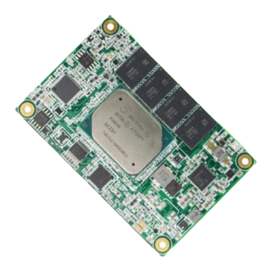
Summary of Contents for Aaeon NanoCOM-APL
- Page 1 NanoCOM-APL COM Express Module User’s Manual 2 Last Updated: May 10, 2019...
- Page 2 AAEON assumes no liabilities resulting from errors or omissions in this document, or from the use of the information contained herein. AAEON reserves the right to make changes in the product design without notice to its users.
- Page 3 Acknowledgement All other product names or trademarks are properties of their respective owners. No ownership is implied or assumed for products, names or trademarks not herein listed by the publisher of this document. Microsoft Windows is a registered trademark of Microsoft Corp. ...
- Page 4 Packing List Before setting up your product, please make sure the following items have been shipped: Item Quantity NanoCOM-APL-A11 Screws If any of these items are missing or damaged, please contact your distributor or sales representative immediately. Preface...
- Page 5 (if any), its specifications, dimensions, jumper/connector settings/definitions, and driver installation instructions (if any), to facilitate users in setting up their product. Users may refer to the AAEON.com for the latest version of this document. Preface...
- Page 6 Safety Precautions Please read the following safety instructions carefully. It is advised that you keep this manual for future references All cautions and warnings on the device should be noted. Make sure the power source matches the power rating of the device. Position the power cord so that people cannot step on it.
- Page 7 If any of the following situations arises, please the contact our service personnel: Damaged power cord or plug Liquid intrusion to the device iii. Exposure to moisture Device is not working as expected or in a manner as described in this manual The device is dropped or damaged Any obvious signs of damage displayed on the device...
- Page 8 FCC Statement This device complies with Part 15 FCC Rules. Operation is subject to the following two conditions: (1) this device may not cause harmful interference, and (2) this device must accept any interference received including interference that may cause undesired operation.
- Page 9 China RoHS Requirements (CN) 产品中有毒有害物质或元素名称及含量 AAEON Main Board/ Daughter Board/ Backplane 有毒有害物质或元素 部件名称 铅 汞 镉 六价铬 多溴联苯 多溴二苯醚 (Pb) (Hg) (Cd) (Cr(VI)) (PBB) (PBDE) 印刷电路板 × ○ ○ ○ ○ ○ 及其电子组件 外部信号 × ○ ○ ○ ○ ○...
- Page 10 China RoHS Requirement (EN) Poisonous or Hazardous Substances or Elements in Products AAEON Main Board/ Daughter Board/ Backplane Poisonous or Hazardous Substances or Elements Hexavalent Polybrominated Polybrominated Component Lead Mercury Cadmium Chromium Biphenyls Diphenyl Ethers (Pb) (Hg) (Cd) (Cr(VI)) (PBB) (PBDE) PCB &...
-
Page 11: Table Of Contents
Table of Contents Chapter 1 - Product Specifications..................1 Specifications ......................2 Chapter 2 – Hardware Information ..................4 Dimensions, Jumpers and Connectors ............... 5 List of Switches and Connectors................7 2.2.1 ROW A/B Connector (CN3) ..............7 Chapter 3 - AMI BIOS Setup ....................12 System Test and Initialization ................ - Page 12 3.5.1.1 North Bridge: LVDS Panel Configuration ......35 3.5.2 Chipset: South Bridge ................38 3.5.2.1 South Bridge: PCI Express Configuration ....... 39 Setup submenu: Security ..................40 Setup submenu: Boot ....................41 Setup submenu: Save & Exit ................43 Chapter 4 – Drivers Installation .................... 44 Driver Download and Installation...............
-
Page 13: Chapter 1 - Product Specifications
Chapter 1 Chapter 1 - Product Specifications... -
Page 14: Specifications
Specifications System Form Factor COM Express Mini size, Type 10 Onboard Intel® Atom™/Celeron®/Pentium® CPU Frequency E39xx series, N4xxx series up to 2.5 GHz Chipset Intel® Atom™/Celeron®/Pentium® Processor Memory Type Onboard LPDDR4 4GB (default), 8GB (optional) Max. Memory Capacity 8GB LPDDR4 Onboard BIOS AMI BIOS, Legacy free Wake on LAN... - Page 15 System MTBF (Hours) 80,000 Certification CE/FCC Class A Display Display Controller Intel® HD Graphics 500/505 Video Output LVDS LCD/eDP, DDI x 1 LVDS Interface Supports 18bit and 24bit Single channel Intel® I210IT Ethernet High Definition Audio Interface Audio USB 2.0 x 8, USB 3.0 x 2 USB Support TX/RX x 2 Serial Port...
-
Page 16: Chapter 2 - Hardware Information
Chapter 2 Chapter 2 – Hardware Information... -
Page 17: Dimensions, Jumpers And Connectors
Dimensions, Jumpers and Connectors Component Side Chapter 2 – Hardware Information... - Page 18 Solder Side With heat spreader Chapter 2 – Hardware Information...
-
Page 19: List Of Switches And Connectors
List of Switches and Connectors Please refer to the table below for all of the board’s jumpers that you can configure for your application Label Function ROW A/B 2.2.1 ROW A/B Connector (CN3) Row A Row B GND (FIXED) GND (FIXED) GBE0_MDI3- GBE0_ACT# GBE0_MDI3+... - Page 20 Row A Row B SATA0_TX- SATA1_TX- SUS_S4# SUS_STAT# SATA0_RX+ SATA1_RX+ SATA0_RX- SATA1_RX- GND (FIXED) GND (FIXED) USB3_RXN0 USB3_TXN0 USB3_RXP0 USB3_TXP0 SUS_S4# PWR_OK USB3_RX1_N USB3_TX1_N USB3_RX1_P USB3_TX1_P BATLOW# ATA_ACT# AC_SYNC AC_SDIN1 AC_RST# AC_SDIN0 GND (FIXED) GND (FIXED) AC_BITCLK SPKR AC_SDOUT I2C_CK BIOS_DIS0# I2C_DAT THRMTRIP#...
- Page 21 Row A Row B USB2+ USB3+ USB_2_3_OC# USB_0_1_OC# USB0- USB1- USB0+ USB1+ VCC_RTC EXCD1_PERST# EXCD0_PERST# EXCD1_CPPE# EXCD0_CPPE# SYS_RESET# LPC_SERIRQ CB_RESET# GND (FIXED) GND (FIXED) GPI0 GPO1 GPO2 PCIE_TX3+ PCIE_RX3+ PCIE_TX3- PCIE_RX3- GND (FIXED) GND (FIXED) PCIE_TX2+ PCIE_RX2+ PCIE_TX2- PCIE_RX2- GPI1 GPO3 PCIE_TX1+ PCIE_RX1+...
- Page 22 Row A Row B PCIE_TX0- PCIE_RX0- GND (FIXED) GND (FIXED) LVDS_A0+( EDP_TX2_P) DDI0_PAIR0+ LVDS_A0-( EDP_TX2_N) DDI0_PAIR0- LVDS_A1+( EDP_TX1_P) DDI0_PAIR1+ LVDS_A1-( EDP_TX1_N) DDI0_PAIR1- LVDS_A2+( EDP_TX0_P) DDI0_PAIR2+ LVDS_A2-( EDP_TX0_N) DDI0_PAIR2- LVDS_VDD_EN(EDP_VDDEN_3_3) LVDS_A3+ LVDS_A3- LVDS_BKLD_EN(EDP_BKLTEN_3_3) GND (FIXED) GND (FIXED) LVDS_A_CK+( EDP_TX3_P) DDI0_PAIR3+ LVDS_A_CK-( EDP_TX3_N) DDI0_PAIR3- LVDS_I2C_CK(EDP_AUXP) LVDS_BKLT_CTRL...
- Page 23 Row A Row B SPI_MOSI DDI0_DDC_AUX_SEL TYPE10# SPI_CS# RS1_TX DDI0_CTRL_CLK RS1_RX DDI0_CTRL_DATA A100 GND (FIXED) B100 GND (FIXED) A101 RS2_TX B101 FAN_PWMOUT A102 RS2_RX B102 FAN_TACHIN A103 LID# B103 SLEEP# A104 VCC_12V B104 VCC_12V A105 VCC_12V B105 VCC_12V A106 VCC_12V B106 VCC_12V A107...
-
Page 24: Chapter 3 - Ami Bios Setup
Chapter 3 Chapter 3 - AMI BIOS Setup... -
Page 25: System Test And Initialization
System Test and Initialization The system uses certain routines to perform testing and initialization during the boot up sequence. If an error, fatal or non-fatal, is encountered, the system will output a few short beeps or an error message. The board can usually continue the boot up sequence with non-fatal errors. -
Page 26: Ami Bios Setup
AMI BIOS Setup The AMI BIOS ROM has a pre-installed Setup program that allows users to modify basic system configurations, which is stored in the battery-backed CMOS RAM and BIOS NVRAM so that the information is retained when the power is turned off. To enter BIOS Setup, press <Del>... -
Page 27: Setup Submenu: Main
Setup submenu: Main Chapter 3 – AMI BIOS Setup... -
Page 28: Setup Submenu: Advanced
Setup submenu: Advanced Chapter 3 – AMI BIOS Setup... -
Page 29: Advanced: Cpu Configuration
3.4.1 Advanced: CPU Configuration Options Summary C-states Disabled Optimal Default, Failsafe Default Enabled Enable / Disable C states. EIST Disabled Enabled Optimal Default, Failsafe Default Enable / Disable Intel speedstep. Turbo Mode Disabled Enabled Optimal Default, Failsafe Default Turbo Mode. Table Continues on Next Page Chapter 3 –... - Page 30 Options Summary Intel Virtualization Disabled Technology Enabled Optimal Default, Failsafe Default When enabled, a VMM can utilize the additional hardware capabilities provided by Vanderpool Technology. VT-d Disabled Optimal Default, Failsafe Default Enabled Enable / Disable CPU VT-d. Thermal Monitor Disabled Enabled Optimal Default, Failsafe Default Enable / Disable Thermal Monitor.
-
Page 31: Advanced: Sata Configuration
3.4.2 Advanced: SATA Configuration Options Summary Chipset SATA Enabled Optimal Default, Failsafe Default Disabled Enable or Disable the Chipset SATA Controller. The Chipset SATA Controller support the 2 black internal SATA ports ( up to 3Gb/s supported per port ). Port 0 Disabled Enabled... -
Page 32: Advanced: Camera Configuration
3.4.3 Advanced: Camera Configuration Options Summary IPU Enable / Disable Optimal Default, Failsafe Default Disable Enable Enable/Disable IPU Device, Please enable IPU first if you want enable camera. Chapter 3 – AMI BIOS Setup... -
Page 33: Advanced: On-Module Hardware Monitor
3.4.4 Advanced: On-Module Hardware Monitor Chapter 3 – AMI BIOS Setup... -
Page 34: Fan 1 Mode Configuration: Full Mode
3.4.4.1 Fan 1 Mode Configuration: Full Mode Options Summary CPU Smart Fan Full Mode Optimal Default, Failsafe Default control Manual Mode by PWM Auto Mode by PWM PWM signal Non-inverting Optimal Default, Failsafe Default Inverting Select output PWM of inverting or non-inverting signal Chapter 3 –... -
Page 35: Fan Mode Configuration: Manual Mode By Pwm
3.4.4.2 Fan Mode Configuration: Manual Mode by PWM Options Summary Manual Setting Optimal Default, Failsafe Default Set Fan at fixed Duty-Cycle Min=0 Max=100 Please input Dec number: PWM signal Non-inverting Optimal Default, Failsafe Default Inverting Select output PWM of inverting or non-inverting signal Chapter 3 –... -
Page 36: Fan Mode Configuration: Auto Mode By Pwm
3.4.4.3 Fan Mode Configuration: Auto Mode by PWM Options Summary PWM signal Non-inverting Optimal Default, Failsafe Default Inverting Select output PWM of inverting or non-inverting signal Monitor Thermal Thermal Source 1(T1) Optimal Default, Failsafe Default Thermal Source 2(T2) Select monitor thermal source Temperature of Optimal Default, Failsafe Default Start... - Page 37 Options Summary Start PWM Optimal Default, Failsafe Default Start PWM Slope (PWM) 0 (PWM) 1 (PWM) Optimal Default, Failsafe Default 2 (PWM) 4 (PWM) 8 (PWM) 16 (PWM) 32 (PWM) 64 (PWM) Slope (PWM) Chapter 3 – AMI BIOS Setup...
-
Page 38: Advanced: On-Module Features
3.4.5 Advanced: On-Module FEATURES Options Summary Battery Management Disable Optimal Default, Failsafe Default One battery Enable to support battery in ACPI OS by I2C_CK, I2C_DAT( B33, B34 ) Chapter 3 – AMI BIOS Setup... -
Page 39: Advanced: Sio Configuration
3.4.6 Advanced: SIO Configuration Chapter 3 – AMI BIOS Setup... -
Page 40: Sio Configuration: Serial Port 1 Configuration
3.4.6.1 SIO Configuration: Serial Port 1 Configuration Options Summary Use This Device Disabled Enabled Optimal Default, Failsafe Default Enable/Disable this Logical Device Possible: Use Automatic Settings Optimal Default, Failsafe Default IO=3F8; IRQ=4; DMA; IO=2C8; IRQ=11; DMA; Allow user to change Device’s Resource settings. New settings will be reflected on This Setup Page after System restarts. -
Page 41: Sio Configuration: Serial Port 2 Configuration
3.4.6.2 SIO Configuration: Serial Port 2 Configuration Options Summary Use This Device Disabled Enabled Optimal Default, Failsafe Default Enable/Disable this Logical Device Possible: Use Automatic Settings Optimal Default, Failsafe Default IO=2F8; IRQ=3; DMA; IO=2D8; IRQ=10; DMA; Allow user to change Device’s Resource settings. New settings will be reflected on This Setup Page after System restarts. -
Page 42: Advanced: Power Management
3.4.7 Advanced: Power Management Options Summary Power Mode ATX Type Optimal Default, Failsafe Default AT Type Select power supply mode. Restore AC Power Last State Loss Always On Always Off Optimal Default, Failsafe Default Select power state when power is re-applied after a power failure. RTC wake system Disabled Optimal Default, Failsafe Default... -
Page 43: Advanced: Digital Io Port Configuration
3.4.8 Advanced: Digital IO Port Configuration Options Summary GPI* Output Input Set DIO as Input or Output Interrupt Disable Optimal Default, Failsafe Default Enable Enable interrupt function with low pulse mode. This triggered pulse needs more than the 10ms. GPO* Output Input Set DIO as Input or Output... - Page 44 Options Summary Output Level High Optimal Default, Failsafe Default Set output level when DIO pin is output Chapter 3 – AMI BIOS Setup...
-
Page 45: Setup Submenu: Chipset
Setup submenu: Chipset Chapter 3 – AMI BIOS Setup... -
Page 46: Chipset: North Bridge
3.5.1 Chipset: North Bridge Options Summary Total Memory 2048 MB ( LPDDR4 ) LVDS Panel Configure LVDS panel parameters. Configuration Chapter 3 – AMI BIOS Setup... -
Page 47: North Bridge: Lvds Panel Configuration
3.5.1.1 North Bridge: LVDS Panel Configuration Options Summary Panel Type 640x480@60Hz 800x480@60Hz 800x600@60Hz 1024x600@60Hz 1024x768@60Hz Optimal Default, Failsafe Default 1280x768@60Hz 1280x800@60Hz 1280x1024@60Hz 1366x768@60Hz 1440x900@60Hz Chapter 3 – AMI BIOS Setup... - Page 48 Options Summary Panel Type 1600x1200@60Hz 1920x1080@60Hz 1920x1200@,60Hz Select panel type. Color Depth 18-bit Optimal Default, Failsafe Default 24-bit 36-bit 48-bit Select panel type Backlight Type Normal Optimal Default, Failsafe Default Inverted Select backlight control signal type Backlight Level Optimal Default, Failsafe Default 100% Select backlight control level Table continues on Next Page...
- Page 49 Options Summary Backlight PWM Freq 100Hz 200Hz 220Hz Optimal Default, Failsafe Default 500Hz 1KHz 2.2KHz 6.5KHz Select PWM frequency of backlight control signal Chapter 3 – AMI BIOS Setup...
-
Page 50: Chipset: South Bridge
3.5.2 Chipset: South Bridge Chapter 3 – AMI BIOS Setup... -
Page 51: South Bridge: Pci Express Configuration
3.5.2.1 South Bridge: PCI Express Configuration Options Summary PCIE_* Port Disabled Enabled Optimal Default, Failsafe Default Control the PCI Express Root Port. AUTO : To disable unused root port automatically for the most optimum power savings. Enable : Enable PCIe root port. Disable : Disable PCIe root port. -
Page 52: Setup Submenu: Security
Setup submenu: Security Change User/Administrator Password You can set an Administrator Password or User Password. An Administrator Password must be set before you can set a User Password. The password will be required during boot up, or when the user enters the Setup utility. A User Password does not provide access to many of the features in the Setup utility. -
Page 53: Setup Submenu: Boot
Setup submenu: Boot Options Summary Quiet Boot Disabled Enabled Optimal Default, Failsafe Default Enable / Disable Quiet Boot option. Monitor Disabled Enabled Optimal Default, Failsafe Default Enable / Disable Monitor Mwait. To install Linux OS, please set this item to disable. Ipv4 PXE Support Disabled Optimal Default, Failsafe Default... - Page 54 Options Summary SCC SD Card Support Disabled Optimal Default, Failsafe Default Enabled SD card support requires HW change. Contact your AAEON Tech support or Contact your AAEON Support for detail. SCC eMMC Support Disabled Enabled Optimal Default, Failsafe Default Enable / Disable eMMC Support.
-
Page 55: Setup Submenu: Save & Exit
Setup submenu: Save & Exit Save Change and Reset Reset the system after saving the changes. Discard Changes and Exit Exit system setup without saving any changes. Restore Defaults Restore / Load Default values for all the setup options. Chapter 3 – AMI BIOS Setup... -
Page 56: Chapter 4 - Drivers Installation
Chapter 4 Chapter 4 – Drivers Installation... -
Page 57: Driver Download And Installation
Driver Download and Installation Drivers for the NanoCOM-APL can be downloaded from the product page on the AAEON website by following this link: https://www.aaeon.com/en/p/com-express-modules-nanocom-apl Download the driver(s) you need and follow the steps below to install them. Step 1 – Install Chipset Drivers Open the Step1 –... - Page 58 Step 5 – Install TXE Drivers Open the Step5 - TXE folder followed by Setup TXE.exe Follow the instructions Drivers will be installed automatically Step 6 – Install Serial I/O Drivers Open the Step6 – Serial IO folder. Follow the instructions in README.txt to setup and verify installation. Step 7 –...
-
Page 59: Appendix A - Watchdog Timer Programming
Appendix A Appendix A - Watchdog Timer Programming... -
Page 60: Watchdog Timer Initial Program
Watchdog Timer Initial Program Table 1 : Embedded BRAM relative register table Default Value Note Index 0x284(Note1) BRAM Index Register Data 0x285(Note2) BRAM Data Register Logical Device Number 0xA8(Note3) Watch dog Logical Device Number Function and Device Number 0x00(Note4) Watch dog Function/Device Number Table 2 : Watchdog relative register table Option Register BitNum... - Page 61 ************************************************************************************ // Embedded BRAM relative definition (Please reference to Table 1) #define byte EcBRAMIndex //This parameter is represented from Note1 #define byte EcBRAMData //This parameter is represented from Note2 #define byte BRAMLDNReg //This parameter is represented from Note3 #define byte BRAMFnDataReg //This parameter is represented from Note4 #define void EcBRAMWriteByte(byte Offset, byte Value);...
- Page 62 ************************************************************************************ Main VOID // Procedure : AaeonWDTConfig // (byte)Timer : Time of WDT timer.(0x00~0xFF) // (boolean)Unit : Select time unit(0: second, 1: minute). AaeonWDTConfig(); // Procedure : AaeonWDTEnable // This procudure will enable the WDT counting. AaeonWDTEnable(); ************************************************************************************ Appendix A – Watchdog Timer Programming...
- Page 63 ************************************************************************************ // Procedure : AaeonWDTEnable AaeonWDTEnable () VOID WDTEnableDisable( // Procedure : AaeonWDTConfig AaeonWDTConfig () VOID // Disable WDT counting WDTEnableDisable( // WDT relative parameter setting WDTParameterSetting(); WDTEnableDisable(byte Value) VOID ECBRAMWriteByte(TimerReg , Value); WDTParameterSetting() VOID Byte TempByte; // Watchdog Timer counter setting ECBRAMWriteByte(TimerReg , TimerVal);...
- Page 64 ************************************************************************************ ECBRAMWriteByte(byte OPReg, byte OPBit, byte Value) VOID IOWriteByte(EcBRAMIndex, 0x10); IOWriteByte(EcBRAMData, BRAMLDNReg); IOWriteByte(EcBRAMIndex, 0x11); IOWriteByte(EcBRAMData, BRAMFnDataReg); IOWriteByte(EcBRAMIndex, 0x13 + OPReg); IOWriteByte(EcBRAMData, Value); IOWriteByte(EcBRAMIndex, 0x12); IOWriteByte(EcBRAMData, 0x30); //Write start ECBRAMReadByte(byte OPReg) Byte IOWriteByte(EcBRAMIndex, 0x10); IOWriteByte(EcBRAMData, BRAMLDNReg); IOWriteByte(EcBRAMIndex, 0x11); IOWriteByte(EcBRAMData, BRAMFnDataReg); IOWriteByte(EcBRAMIndex, 0x12); IOWriteByte(EcBRAMData, 0x10);...
-
Page 65: Appendix B - I/O Information
Appendix B Appendix B - I/O Information... -
Page 66: I/O Address Map
I/O Address Map Appendix B – I/O Information... -
Page 67: Memory Address Map
Memory Address Map Appendix B – I/O Information... -
Page 68: Irq Mapping Chart
IRQ Mapping Chart Appendix B – I/O Information... -
Page 69: Appendix C - Programming Digital I/O
Appendix C Appendix C – Programming Digital I/O... -
Page 70: Di/O Programming
DI/O Programming NanoCOM-APL utilizes AAEON chipset as its Digital I/O controller. Below are the procedures to complete its configuration which you can develop customized program to fit your application. Appendix C –Programming Digital I/O... -
Page 71: Digital I/O Register
Digital I/O Register Table 1 : Embedded BRAM relative register table Default Value Note Index 0x284(Note1) BRAM Index Register Data 0x285(Note2) BRAM Data Register Logical Device Number 0xA2(Note3) Watch dog Logical Device Number IO Direction DIO Input/Output Function/Device Function and Device 0x00(Note4) Number Number... -
Page 72: Digital I/O Sample Program
Digital I/O Sample Program ************************************************************************************ // Embedded BRAM relative definition (Please reference to Table 1) #define byte EcBRAMIndex //This parameter is represented from Note1 #define byte EcBRAMData //This parameter is represented from Note2 #define byte BRAMLDNReg //This parameter is represented from Note3 #define byte BRAMFnData0Reg //This parameter is represented from Note4 #define byte BRAMFnData1Reg //This parameter is represented from Note5 #define void EcBRAMWriteByte(byte Offset, byte Value);... - Page 73 ************************************************************************************ Main VOID Boolean PinStatus ; // Procedure : AaeonReadPinStatus // Input : Example, Read Digital I/O Pin 3 status // Output : InputStatus : 0: Digital I/O Pin level is low 1: Digital I/O Pin level is High PinStatus = AaeonReadPinStatus(DIO0ToDIO7Reg, DIO3Bit); // Procedure : AaeonSetOutputLevel // Input : Example, Set Digital I/O Pin 6 level...
- Page 74 ************************************************************************************ AaeonReadPinStatus(byte OptionReg, byte BitNum) Boolean Byte TempByte; TempByte = ECBRAMReadByte(BRAMFnData1Reg, OptionReg); If (TempByte & BitNum == 0) Return 0; Return 1; AaeonSetOutputLevel(byte OptionReg, byte BitNum, byte Value) VOID Byte TempByte; TempByte = ECBRAMReadByte(BRAMFnData1Reg, OptionReg); TempByte |= (Value << BitNum); ECBRAMWriteByte(OptionReg, BitNum, Value);...
- Page 75 ************************************************************************************ ECBRAMWriteByte(byte OPReg, byte OPBit, byte Value) VOID IOWriteByte(EcBRAMIndex, 0x10); IOWriteByte(EcBRAMData, BRAMLDNReg); IOWriteByte(EcBRAMIndex, 0x11); IOWriteByte(EcBRAMData, BRAMFnDataReg); IOWriteByte(EcBRAMIndex, 0x13 + OPReg); IOWriteByte(EcBRAMData, Value); IOWriteByte(EcBRAMIndex, 0x12); IOWriteByte(EcBRAMData, 0x30); //Write start ECBRAMReadByte(byte FnDataReg, byte OPReg) Byte IOWriteByte(EcBRAMIndex, 0x10); IOWriteByte(EcBRAMData, BRAMLDNReg); IOWriteByte(EcBRAMIndex, 0x11); IOWriteByte(EcBRAMData, FnDataReg); IOWriteByte(EcBRAMIndex, 0x12);...
Need help?
Do you have a question about the NanoCOM-APL and is the answer not in the manual?
Questions and answers