
Subscribe to Our Youtube Channel
Related Manuals for Advantech PCIE-1884


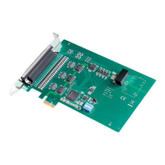
Summary of Contents for Advantech PCIE-1884
- Page 1 User Manual PCIE-1884 32-Bit, 4-Channel Encoder Counter with Preloaded Position Comparison FIFO PCI Express Card...
- Page 2 No part of this manual may be reproduced, copied, translated, or transmitted in any form or by any means without the prior written permission of Advantech Co., Ltd. The information provided in this manual is intended to be accurate and reliable. However, Advantech Co., Ltd.
- Page 3 This product has passed the CE test for environmental specifications when shielded cables are used for external wiring. We recommend the use of shielded cables. This type of cable is available from Advantech. Please contact your local supplier for ordering information.
- Page 4 PCIE-1884 User Manual...
-
Page 5: Table Of Contents
Unpacking Instructions................8 Driver Installation ..................8 Hardware Installation ................9 Device Setup and Configuration ............. 10 Figure 2.1 PCIE-1884 Device Settings ........10 Figure 2.2 Device Settings Page ..........11 Figure 2.3 PCIE-1884 Device Testing ........11 Chapter Signal Connections ......13... - Page 6 PCIE-1884 User Manual...
-
Page 7: Chapter 1 Introduction
Chapter Introduction This chapter provides a brief introduction to the PCIE-1884 card and its typical applications. Features Applications Packing List Software Overview Roadmap Accessories... -
Page 8: Key Features
PCIE-1884 is a PCI Express card that features four 32-bit encoder counters with pro- grammable trigger output (preloaded FIFO) for position comparisons. Ideal for motor control and position monitoring applications, PCIE-1884 also provides general coun- ter functions, such as frequency measurement, pulse width measurement, pulse out- put, and PWM output. -
Page 9: Applications
BoardID Switch The PCIE-1884 card is equipped with a built-in DIP switch for defining each card’s ID when multiple cards are installed on the same PC chassis. The BoardID setting func- tion is very useful when building a system with multiple PCIE-1884 cards. -
Page 10: Software Overview
Software Overview Advantech offers a comprehensive bundle of DLL drivers, third-party drivers, and application software to assist users with leveraging the full benefits of the PCIE-1884 card. Device drivers LabVIEW driver Advantech DAQNavi software Datalogger Programming Choices for Encoder Cards Advantech’s application software, such as Advantech Device Drivers, can be used... -
Page 11: Accessories
To troubleshoot the driver error, check the error code and description against the error control information provided in the DAQNavi SDK manual. Accessories Advantech offers a wide range of accessories for the PCIE-1884 card, as listed below. Wiring Cables ... - Page 12 PCIE-1884 User Manual...
-
Page 13: Chapter 2 Installation
Chapter Installation This chapter provides detailed step-by-step instructions for driver and card installation. Unpacking Instructions Driver Installation Hardware Installation Device Setup and Configuration... -
Page 14: Unpacking Instructions
Unpacking Instructions After receiving the PCIE-1884 product shipment, inspect the package to ensure that you have received the following: 1 x PCIE-1884 card 1 x PCIE-1884 startup manual The PCIE-1884 card contains certain electronic components that are vulnerable to electrostatic discharge (ESD). -
Page 15: Hardware Installation
Hardware Installation After the device driver has been installed, the PCIE-1884 card can be installed in the computer. The steps for installing the card are outlined below. Please refer to the computer’s user manual or related documentation for additional installation advice. -
Page 16: Device Setup And Configuration
API is accessed. Setting Up a Device To install the I/O device for your card, run the Advantech Navigator program (by accessing Start/Programs/Advantech Automation/Navigator for DN4). The device(s) already installed on the system (if any) will be shown in the Installed Devices list. -
Page 17: Figure 2.2 Device Settings
Configuring the Device Navigate to the Device Settings page to configure the PCIE-1884 card. Users can configure not only the counter/PWM output, but also the Digital Input/Out- put. Figure 2.2 Device Settings Page After the card is installed and configured, navigate to the Device Test page to test the hardware using the testing utility supplied. - Page 18 PCIE-1884 User Manual...
-
Page 19: Chapter 3 Signal Connections
Chapter Signal Connections This chapter explains how to con- nect input and output signals to the PCIE-1884 card via the I/O connector. Overview Board ID Settings Signal Connections Field Wiring Considerations... -
Page 20: Overview
This chapter provides useful information about how to connect input and output signals to the PCIE-1884 card via the I/O connector. Switch and Jumper Settings The location of jumpers and switches on the PCIE-1884 card is shown in Figure 3.1. Figure 3.1 Connector and Switch Locations PCIE-1884 User Manual... -
Page 21: Board Id (Sw1)
3.2.1 Board ID (SW1) The PCIE-1884 card features a built-in DIP switch (SW1) that is used to define each card’s board ID. When multiple cards are installed on the same chassis, the board ID switch is used to set each card’s device number. -
Page 22: Signal Connections
Signal Connections Pin Assignments The I/O connector on the PCIE-1884 card is a 37-pin connector that enables users to integrate additional accessories via the PCL-10137H shielded cable. The pin assignments for the 37-pin I/O connector on the PCIE-1884 card are shown in Figure 3.2. -
Page 23: I/O Connector Signal Description
Negative input of gate input (general purpose coun- CNT0_GATE-/Z- ter) or signal Z input (encoder counter) of counter channel 0 Positive input of gate input (general purpose coun- CNT1_GATE+/Z+ ter) or signal Z input (encoder counter) of counter channel 1 PCIE-1884 User Manual... - Page 24 Isolated digital output channel 2 of output of counter IDO2/CNT2_OUT channel 2 Isolated digital output channel 3 of output of counter IDO3/CNT3_OUT channel 3 Power and Ground 1, 14, 17, Reference ground for all signals 32, 35 PCIE-1884 User Manual...
-
Page 25: Field Wiring Considerations
Field Wiring Considerations When using PCIE-1884 cards to acquire data in an outdoor environment, general environmental noise can significantly affect the accuracy of measurements if due cautions are not taken. The following measures can reduce possible interference to signal wires running between signal sources and the PCIE-1884 card. - Page 26 PCIE-1884 User Manual...
-
Page 27: Appendix A Specifications
Appendix Specifications... -
Page 28: Function Block
Opto-Isolator Response Time 100ns VIH (max.) 50 V Input Voltage VIH (min.) VIL (max.) Digital Output Channels 4 (shared with CNTn_OUT pins) 2500 V Optical Isolation Response Time 100 ns Supply Voltage 5V/TTL level Sink/Source Current 24 mA max./channel PCIE-1884 User Manual... -
Page 29: Counter/Timer
3.3 V @ 360 mA, 12 V @ 245 mA Operating 0 ~ 60 °C (32 ~ 140 °F) Temperature Storage -40 ~ 70 °C (-40 ~ 158 °F) Operating 5 ~ 85% RH non-condensing Relative Humidity Storage 5 ~ 95% RH non-condensing Certifications CE/FCC PCIE-1884 User Manual... - Page 30 PCIE-1884 User Manual...
-
Page 31: Appendix B Operation Theory
Appendix Operation Theory... -
Page 32: Digital Input/Output Operation
Digital Input/Output Operation The PCIE-1884 card supports 32 digital I/O channels. Each byte can be used as either an input port or an output port by configuring the corresponding parameter. All four channels of the byte have the same configuration. - Page 33 Pulse Width Measurement Connection The PCIE-1884’s built-in counter can measure the pulse width value of the sig- nal connected to the counter input. The measurable range is 50 ns to 107 sec- onds. Both the logic high time and logic low time can be measured within the measurable range.
- Page 34 PWM Output PCIE-1884 can generate PWM (pulse width modulation) signals. Users can configure the logic high time and logic low time as shown in the figure below. The available period for logic high time and logic low time is 100 ns ~ 214 sec- onds.
- Page 35 A (Source) and B (Aux). The counter increments on each active edge of channel A when channel B is low, and decrements on each active edge of channel A when channel B is high, as shown in the figure below. PCIE-1884 User Manual...
- Page 36 Users can program the width of the generated pulse. The range of the pulse width is from 10 ns to 42.94967295 seconds in step of 10 ns. An example position comparison using quadrature X4 encoding is shown in the figure below. PCIE-1884 User Manual...
- Page 37 PCIE-1884 User Manual...
- Page 38 No part of this publication may be reproduced in any form or by any means, such as electronically, by photocopying, recording, or otherwise, without prior written permission from the publisher. All brand and product names are trademarks or registered trademarks of their respective companies. © Advantech Co., Ltd. 2018...
Need help?
Do you have a question about the PCIE-1884 and is the answer not in the manual?
Questions and answers