
Subscribe to Our Youtube Channel
Related Manuals for NXP Semiconductors 56F8367


Summary of Contents for NXP Semiconductors 56F8367
- Page 1 56F8367 Evaluation Module User Manual 56F8300 16-bit Digital Signal Controllers MC56F8367EVMUM Rev. 2 07/2005 freescale.com...
- Page 2 Document Revision History Version History Description of Change Rev 1.0 Initial Public Release Rev 2.0 Updated look and feel...
-
Page 3: Table Of Contents
TABLE OF CONTENTS Preface Preface-vii Chapter 1 Introduction 56F8367EVM Architecture..........1-2 56F8367EVM Configuration Jumpers . - Page 4 2.13 CAN Interfaces ............2-23 2.13.1 FlexCAN #1 Interface .
- Page 5 LIST OF FIGURES Block Diagram of the 56F8367EVM ........1-2 MC56F8367 Default Jumper Options .
- Page 6 MC56F8367EVM User Manual, Rev. 2 Freescale Semiconductor Preliminary...
- Page 7 LIST OF TABLES 56F8367EVM Default Jumper Options ....... . 1-4 SCI #0 Jumper Options .
- Page 8 2-26 SCI #1 Connector Description ........2-35 2-27 SPI #0 Connector Description .
- Page 9 This document is intended for application developers who are creating software for devices using the Freescale 56F8367 part or a member of the 56F8300 family that is compatible with this part. Examples would include the 56F8346 and the 56F8357 devices.
- Page 10 Notation Conventions This manual uses the following notational conventions: Term or Value Symbol Examples Exceptions Active High Signals No special symbol (Logic One) attached to the signal CLKO name Active Low Signals Noted with an In schematic drawings, (Logic Zero) overbar in text and in Active Low Signals may be most figures...
- Page 11 Evaluation Module; a hardware platform which allows a customer to evaluate the silicon and develop his application FlexCAN Flexable CAN Interface Module; a peripheral on the 56F8367 part GPIO General Purpose Input and Output port on Freescale’s family of controllers;...
- Page 12 The following sources were referenced to produce this manual: [1] DSP56800E Reference Manual, DSP56800ERM, Freescale Semiconductor [2] 56F8300 Peripheral User Manual, MC56F8300UM, Freescale Semiconductor [3] 56F8367 Technical Data, MC56F8367, Freescale Semiconductor [4] CiA Draft Recommendation DR-303-1, Cabling and Connector Pin Assignment, Version 1.0, CAN in Automation [5] CAN Specification 2.0B, BOSCH or CAN in Automation...
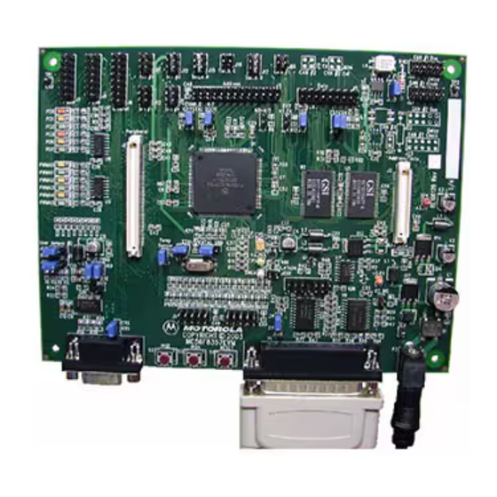
- Page 13 Chapter 1 Introduction The 56F8367EVM is used to demonstrate the abilities of the 56F8367 controller and to provide a hardware tool allowing the development of applications. The 56F8367EVM is an evaluation module board that includes a 56F8367 part, peripheral expansion connectors, a CAN interface, 512KB of external memory and a pair of daughter card connectors.
-
Page 14: 56F8367Evm Architecture
56F8367EVM provides the features necessary for a user to write and debug software, demonstrate the functionality of that software and interface with the user's application-specific device(s). The 56F8367EVM is flexible enough to allow a user to fully exploit the 56F8367's features to optimize the performance of his product, as shown in Figure 1-1. -
Page 15: 56F8367Evm Configuration Jumpers
56F8367EVM Configuration Jumpers 1.2 56F8367EVM Configuration Jumpers Ninteen jumper groups, (JG1-JG19), shown in Figure 1-2, are used to configure various features on the 56F8367EVM board. Table 1-1 describes the default jumper group settings. JG14 JG12 JG13 JG13 JG15 JG17 PWMA0 PWMA1 PWMA2 PWMA3... -
Page 16: 56F8367Evm Default Jumper Options
Table 1-1. 56F8367EVM Default Jumper Options Jumper Jumpers Comment Group Connections Use on-board EXTAL crystal input for oscillator 1–2 Use on-board XTAL crystal input for oscillator 1–2 Enable on-board Parallel JTAG Host/Target Interface Enable Internal Boot Mode 1–2 Enable A0 - A23 for external memory accesses Enable Crystal Mode 1–2 Enable SRAM Memory Bank 0 (use CS0) -
Page 17: 56F8367Evm Connections
56F8367EVM Connections 1.3 56F8367EVM Connections An interconnection diagram is shown in Figure 1-3 for connecting the PC and the external +12.0V DC/AC power supply to the 56F8367EVM board. Parallel extension cable MC56F8367EVM PC-compatible computer Connect cable to parallel / printer port External with 2.1mm, +12V... - Page 18 MC56F8367EVM User Manual, Rev. 2 Freescale Semiconductor Preliminary...
-
Page 19: Technical Summary
Chapter 2 Technical Summary The 56F8367EVM is designed as a versatile development card using the 56F8367 processor, allowing the creation of real-time software and hardware products to support a new generation of applications in servo and motor control, digital and wireless messaging, digital answering machines, feature phones, modems, and digital cameras. - Page 20 • CAN #2 interface, for high speed, 1.0Mbps, FlexCAN communications [U11 and J22] • CAN #2 bypass and bus termination [J23 and JG17] • CAN #2 interface signal isolation [JG14] • Peripheral Daughter Card connector, to allow the user to connect his own SCI, SPI or GPIO-compatible peripheral to the controller [J1] •...
- Page 21 • Address bus expansion connector, to allow the user to monitor the external address bus [J4] • Data bus expansion connector, to allow the user to monitor the external data bus [J5] • External memory bus control signal connector, to allow the user to monitor the external memory bus [J6] •...
-
Page 22: Mc56F8367
The 56F8367EVM uses a Freescale MC56F8367VPY60 part, designated as U1 on the board and in the schematics. This part will operate at a maximum external bus speed of 60MHz. A full description of the 56F8367, including functionality and user information, is provided in these documents: •... -
Page 23: Sram Bank 0
Additionally, CS0 can be configured to assign this memory’s size and starting address to any modulo address space. This memory bank will operate with zero wait state access while the 56F8367 is running at 60MHz and can be disabled by removing the jumper at JG7. -
Page 24: Sram Bank 1
This memory bank will operate with zero wait state access while the 56F8367 is running at 60MHz and can be disabled by removing the jumpers at JG8. -
Page 25: Rs-232 Serial Communications
RS-232 Serial Communications 2.3 RS-232 Serial Communications The 56F8367EVM provides an RS-232 interface by the use of an RS-232 level converter, Maxim MAX3245EEAI, designated as U4. Refer to the RS-232 schematic diagram in Figure 2-3. The RS-232 level converter transitions the SCI port’s +3.3V signal levels to RS-232-compatible signal levels and connects to the host’s serial port via connector P2. -
Page 26: Clock Source
The 56F8367EVM uses an 8.00MHz crystal, Y1, connected to its external crystal inputs, EXTAL and XTAL. To achieve its maximum internal operating frequency, the 56F8367 uses its internal PLL to multiply the input frequency. An external oscillator source can be connected to the processor by using the oscillator bypass connectors, JG1 and JG2;... -
Page 27: Operating Mode
The user can select between a 64K address space or an 8M address space. Refer to the 56F8300 Peripheral User Manual and the 56F8367 Technical Data Sheet for a complete description of the chip’s operating modes. -
Page 28: Clkmode
The user can select between the use of a crystal or an oscillator as the clock source for the processor. Refer to the 56F8300 Peripheral User Manual and the 56F8367 Technical Data Sheet for a complete description of the chip’s operating modes. -
Page 29: Debug Support
Debug Support Setting PC0, PC1, PC2, PC3, PD6, or PD7 to a Logic One value will turn on the associated LED. MC56F8367 INVERTING BUFFER +3.3V RED LED YELLOW LED GREEN LED RED LED YELLOW LED GREEN LED Figure 2-5. Schematic Diagram of the Debug LED Interface 2.7 Debug Support The 56F8367EVM provides an on-board parallel JTAG host target interface and a JTAG interface connector for external target interface support. -
Page 30: Jtag Connector
The JTAG connector on the 56F8367EVM allows the connection of an external host target interface for downloading programs and working with the 56F8367’s registers. This connector is used to communicate with an external host target interface, which passes information and data back and forth with a host processor running a debugger program. -
Page 31: Parallel Jtag Interface Connector
Debug Support 2.7.2 Parallel JTAG Interface Connector The Parallel JTAG Interface Connector, P1, allows the 56F8367 to communicate with a parallel printer port on a Windows PC; reference Figure 2-6. Using this connector, the user can download programs and work with the 56F8367’s registers. -
Page 32: Parallel Jtag Interface Connector Description
Table 2-9. Parallel JTAG Interface Connector Description Pin # Signal Pin # Signal PORT_RESET PORT_IDENT PORT_TMS PORT_TCK PORT_TDI PORT_TRST PORT_DE PORT_IDENT PORT_VCC PORT_TDO PORT_CONNECT Table 2-10. Parallel JTAG Interface Voltage Jumper Selection JG19 Comment 1 - 2 Interface with the PC’s printer port using +3.3V signals 2 - 3 Interface with the PC’s printer port using +5.0V signals MC56F8367EVM User Manual, Rev. -
Page 33: External Interrupts
External Interrupts 2.8 External Interrupts Two on-board push button switches are provided for external interrupt generation, as shown in Figure 2-7. S2 allows the user to generate a hardware interrupt for signal line IRQA. S3 allows the user to generate a hardware interrupt for signal line IRQB. These two switches allow the user to generate interrupts for his user-specific programs. -
Page 34: Reset
2.9 Reset Logic is provided on the 56F8367 to generate an internal power-on reset. Additional reset logic is provided to support the reset signals from the JTAG connector, the parallel JTAG interface and the user reset push button, S1; refer to Figure 2-8. -
Page 35: Power Supply
R72 to R71. Additonally, four zero ohm resistors or shorting wires must be added at R67, R68, R69, and R70 to allow the external +2.5V DC to pass to the 56F8367. +5.0V DC Power +5.0V... -
Page 36: Daughter Card Connectors
2.11 Daughter Card Connectors The EVM board contains two daughter card connectors. One connector, J1, contains the processor’s peripheral port signals. The second connector, J2, contains the processor’s external memory bus signals. 2.11.1 Peripheral Daughter Card Connector The processor’s peripheral port signals are connected to the peripheral daughter card connector, J1. - Page 37 Daughter Card Connectors Table 2-11. Peripheral Daughter Card Connector Description (Continued) Pin # Signal Pin # Signal IRQA IRQB RXD0 / PE1 RXD1 / PD7 PWMB0 PWMB1 PWMB2 PWMB3 PWMB4 PWMB5 ISB0 / PD10 ISB1 / PD11 ISB2 / PD12 FAULTB1 FAULTB0 FAULTB3...
-
Page 38: Memory Daughter Card Connector
Table 2-11. Peripheral Daughter Card Connector Description (Continued) Pin # Signal Pin # Signal REFH REFH GNDA GNDA AN10 AN11 AN12 AN13 AN14 AN15 2.11.2 Memory Daughter Card Connector The processor’s external memory bus signals are connected to the memory daughter card connector, J2. - Page 39 Daughter Card Connectors Table 2-12. Memory Daughter Card Connector Description (Continued) Pin # Signal Pin # Signal D0 / PF9 D15 / PF8 D1 / PF10 D14 / PF7 D2 / PF11 D13 / PF6 D3 / PF12 D12 / PF5 D4 / PF13 D11 / PF4 D5 / PF14...
-
Page 40: Motor Control Pwm Signals And Leds
2.12 Motor Control PWM Signals and LEDs The 56F8367 has two independent groups of dedicated PWM units. Each unit contains six PWM, three phase current sense inputs and four fault input lines. PWM group A’s PWM lines are connected to a set of six PWM LEDs via inverting buffers. The buffers are used to isolate and drive the Processor’s PWM group A’s outputs to the PWM LEDs. -
Page 41: Can Interfaces
The 56F8367EVM board contains a CAN physical-layer interface chip that is attached to the FlexCAN port’s CAN1_RX and CAN1_TX pins on the 56F8367. The EVM board uses a Phillips high-speed, 1.0Mbps, physical layer interface chip, PCA82C250. Due to the +5.0V operating voltage of the CAN interface chip, a pull-up to +5.0V is required to level shift the transmit data... -
Page 42: Flexcan #2 Interface
PCA82C250. Due to the +5.0V operating voltage of the CAN interface chip, a pull up to +5.0V is required to level shift the transmit data output line from the 56F8367. The CAN2H and CAN2L signals pass through inductors before attaching to the CAN bus connectors. A primary, J22, and daisy-chain, J23, CAN connector are provided to allow easy daisy-chaining of CAN devices. -
Page 43: Can #2 Interface
CAN Interfaces +5.0V MC56F8367 CAN Transceiver JG14 PD0 / CAN2_TX CANH CAN #2 Bus Connector CANL PD1 / CAN2_RX PCA82C250 Daisy-Chain CAN #2 Connector JG17 CAN #2 Bus Terminator Figure 2-12. CAN #2 Interface Table 2-14. CAN #2 Header Description J22 and J23 Pin # Signal... -
Page 44: Software Feature Jumpers
2.14 Software Feature Jumpers The 56F8367EVM board contains two software feature jumpers that allow the user to select user-defined software features. Two GPIO port pins, PE4 and PE7, are pulled high or low with 10K ohm resistors on JG15 and JG16. Attaching a jumper between pins 1 and 2 will place a high or 1 on the port pin. -
Page 45: Peripheral Expansion Connectors
2.15 Peripheral Expansion Connectors The EVM board contains a group of peripheral expansion connectors used to gain access to the resources of the 56F8367. The following signal groups have expansion connectors: • External Memory Address Bus (A0 - A23) General Purpose Port A (bits 0 - 13) General Purpose Port E (bits 2 &... -
Page 46: Address Bus Expansion Connector
2.15.1 Address Bus Expansion Connector The address bus expansion connector contains the 56F8367’s 24 external memory address signal lines. Address lines A6 and A7 can optionally be used as GPIO Port E lines (bits 2 and 3). Address lines A8 - A15 can optionally be used as GPIO Port A lines (bits 0 - 7). Address lines A0 - A5 can optionally be used as GPIO Port A lines (bits 8 - 13). -
Page 47: Data Bus Expansion Connector
Peripheral Expansion Connectors 2.15.2 Data Bus Expansion Connector The data bus expansion connector contains the 56F8367’s 16 external memory data signal lines. Refer to Table 2-17 for the data bus connector information. Data lines D0 - D15 can also be used as GPIO Port F lines (bits 0 - 15). -
Page 48: External Memory Control Signal Expansion Connector
2.15.3 External Memory Control Signal Expansion Connector The external memory control signal connector contains the 56F8367’s external memory control signal lines. CS2 and CS3 are MPIO signals, which can be configured as GPIO Port D lines (bits 0 and 1). Refer to Table 2-18 for the names of these signals. -
Page 49: Encoder #1 / Spi #1 Expansion Connector
Peripheral Expansion Connectors 2.15.5 Encoder #1 / SPI #1 Expansion Connector The Encoder #1 / SPI #1 port is an MPIO port attached to the SPI #1 expansion connector. This port can be configured as a Quadrature Decoder interface port, a Serial Peripherial Interface, Quad Timer port or General Purpose I/O port. -
Page 50: Timer Channel D Expansion Connector
2.15.7 Timer Channel D Expansion Connector The Timer Channel D port is a Quad Timer attached to the Timer D expansion connector. This port can be configured as a Quad Timer port or a General Purpose I/O port. Refer to Table 2-22 for the signals attached to the connector. -
Page 51: A/D Port A Expansion Connector
Peripheral Expansion Connectors 2.15.8 A/D Port A Expansion Connector The eight-channel Analog-to-Digital conversion Port A is attached to this connector. Refer to Table 2-23 for connection information. There is a Resistor/Connector (R/C) network on each of the Analog Port A input signals; see Figure 2-14. -
Page 52: A/D Port B Expansion Connector
2.15.9 A/D Port B Expansion Connector The eight-channel Analog-to-Digital conversion Port B is attached to this connector. Refer to Table 2-24 for connection information. There is an R/C network on each of the Analog Port B input signals; see Figure 2-14. -
Page 53: Serial Communications Port #1 Expansion Connector
Peripheral Expansion Connectors 2.15.11 Serial Communications Port #1 Expansion Connector The Serial Communications Port #1 is an MPIO port attached to the SCI #1 expansion connector. This port can be configured as a Serial Communications Interface or as a General Purpose I/O port. -
Page 54: Flexcan #1 Expansion Connector
2.15.13 FlexCAN #1 Expansion Connector The FlexCAN Port #1 is attached to this connector. Refer to Table 2-28 for connection information. Table 2-28. CAN #1 Connector Description Pin # Signal Pin # Signal CAN1_TX CAN1_RX 2.15.14 FlexCAN #2 Expansion Connector The FlexCAN Port #2 is attached to this connector. -
Page 55: Pwm Port A Expansion Connector
Peripheral Expansion Connectors 2.15.15 PWM Port A Expansion Connector The PWM Port A is attached to this connector. Refer to Table 2-30 for connection information. Table 2-30. PWM Port A Connector Description Pin # Signal Pin # Signal PWMA0 PWMA1 PWMA2 PWMA3 PWMA4... -
Page 56: Test Points
2.16 Test Points The 56F8367EVM board has a total of seven test points: • Analog Ground (AGND) • Three Digital Grounds (GND) • +3.3V • +3.3VA • +5.0V MC56F8367EVM User Manual, Rev. 2 2-38 Freescale Semiconductor Preliminary... -
Page 57: 56F8367Evm Schematics
Appendix A 56F8367EVM Schematics 56F8367EVM Schematics, Rev. 2 Freescale Semiconductor Appendix A-1 Preliminary... - Page 58 MC56F8367EVM User Manual, Rev. 2 Appendix A-2 Freescale Semiconductor Preliminary...
- Page 59 56F8367EVM Schematics, Rev. 2 Freescale Semiconductor Appendix A-3 Preliminary...
- Page 60 MC56F8367EVM User Manual, Rev. 2 Appendix A-4 Freescale Semiconductor Preliminary...
- Page 61 56F8367EVM Schematics, Rev. 2 Freescale Semiconductor Appendix A-5 Preliminary...
- Page 62 MC56F8367EVM User Manual, Rev. 2 Appendix A-6 Freescale Semiconductor Preliminary...
- Page 63 56F8367EVM Schematics, Rev. 2 Freescale Semiconductor Appendix A-7 Preliminary...
- Page 64 MC56F8367EVM User Manual, Rev. 2 Appendix A-8 Freescale Semiconductor Preliminary...
- Page 65 56F8367EVM Schematics, Rev. 2 Freescale Semiconductor Appendix A-9 Preliminary...
- Page 66 MC56F8367EVM User Manual, Rev. 2 Appendix A-10 Freescale Semiconductor Preliminary...
- Page 67 56F8367EVM Schematics, Rev. 2 Freescale Semiconductor Appendix A-11 Preliminary...
- Page 68 MC56F8367EVM User Manual, Rev. 2 Appendix A-12 Freescale Semiconductor Preliminary...
- Page 69 56F8367EVM Schematics, Rev. 2 Freescale Semiconductor Appendix A-13 Preliminary...
- Page 70 MC56F8367EVM User Manual, Rev. 2 Appendix A-14 Freescale Semiconductor Preliminary...
- Page 71 56F8367EVM Schematics, Rev. 2 Freescale Semiconductor Appendix A-15 Preliminary...
- Page 72 MC56F8367EVM User Manual, Rev. 2 Appendix A-16 Freescale Semiconductor Preliminary...
- Page 73 Appendix B 56F8367EVM Bill of Material Description Ref. Designators Vendor Part # Integrated Circuits MC56F8367 Freescale, MC56F8367VPY60 128K x 16-Bit SRAM U2, U3 GSI, GS72116ATP-8 RS-232 Transceiver Maxim, MAX3245EEAI 74AC04 U5, U6 ON Semiconductor, MC74AC04AD 74AC00 Fairchild, 74AC00SC 74HC244 ON Semiconductor, MC74LHC44AADW 74LCX244 ON Semiconductor, MC74LCX244ADW CAN Transceiver...
- Page 74 Description Ref. Designators Vendor Part # Resistors (Continued) 5.1KΩ R42 - R48 SMEC, RC73L2A512OHMJT 51Ω R50, R51 SMEC, RC73L2A51OHMJT 270Ω R52 - R64 SMEC, RC73L2A271OHMJT 10Ω SMEC, RC73L2A100OHMJT 0Ω R66, R72 - R77 SMEC, RC73JP2A 0Ω R67 - R71 (Optional) SMEC, RC73JP2A 100Ω...
- Page 75 Description Ref. Designators Vendor Part # Capacitors (Continued) 0.001µF SMEC, MCCE102K2NR-T1 100pF SMEC, MCCE101K2NR-T1 0.0022µF C59 - C74 SMEC, MCCE222K2NR-T1 10µF, +10V DC KEMET, T494B106M010AS Jumpers 3 × 1 Bergstick JG1, JG15, JG16, JG19 SAMTEC, TSW-103-07-S-S 1 × 2 Bergstick JG2 - JG7, JG10 - JG13, JG17, SAMTEC, TSW-102-07-S-S JG18...
- Page 76 Description Ref. Designators Vendor Part # Connectors (Continued) 9 x 2 Header SAMTEC, TSW-106-09-S-D 8 x 2 Header SAMTEC, TSW-106-08-S-D 7 x 2 Header J7, J8 SAMTEC, TSW-106-07-S-D 5 x 2 Header J9, J10, J20 - J23 SAMTEC, TSW-106-05-S-D 3 x 2 Header J11 - J15, J17 SAMTEC, TSW-106-03-S-D 2 x 2 Header...
- Page 77 INDEX Numerics 1.2 Amp power supply 2-17 FlexCAN Preface-ix 56F8300 Peripheral User Manual FlexCAN Interface Module 56F8357 Technical Data Sheet FlexCAN Preface-ix 8.00MHz crystal oscillator FSRAM Preface-ix General Purpose Input and Output Preface-ix GPIO Preface-ix Analog-to-Digital GPIO Preface-ix 2-28 Preface-ix Analog-to-Digital Converter Preface-ix Host Parallel Interface Connector...
- Page 78 Preface-ix Preface-x Light Emitting Diode Preface-x Preface-ix Random Access Memory Low-profile Quad Flat Package Preface-x LQFP Preface-ix Read-Only Memory LQFP Preface-ix Preface-x real-time debugging 2-10 Resistor/Capacitor Network Preface-x MPIO Preface-ix 2-31 Preface-x Multi Purpose Input and Output RS-232 MPIO Preface-ix level converter schematic diagram On-board power regulation...
- Page 80 How to Reach Us: Home Page: www.freescale.com E-mail: support@freescale.com USA/Europe or Locations Not Listed: Freescale Semiconductor Technical Information Center, CH370 1300 N. Alma School Road Chandler, Arizona 85224 +1-800-521-6274 or +1-480-768-2130 support@freescale.com Europe, Middle East, and Africa: Freescale Halbleiter Deutschland GmbH Technical Information Center Schatzbogen 7 81829 Muenchen, Germany...
- Page 81 Mouser Electronics Authorized Distributor Click to View Pricing, Inventory, Delivery & Lifecycle Information: MC56F8367EVME MC56F8367EVM DEMO56F8013...
Need help?
Do you have a question about the 56F8367 and is the answer not in the manual?
Questions and answers