
Subscribe to Our Youtube Channel
Related Manuals for OLIMEX LPC-E2468


Summary of Contents for OLIMEX LPC-E2468
-
Page 1: Users Manual
LPC-E2468 development board Users Manual Rev.B, February 2008 Copyright(c) 2008, OLIMEX Ltd, All rights reserved... -
Page 2: Board Features
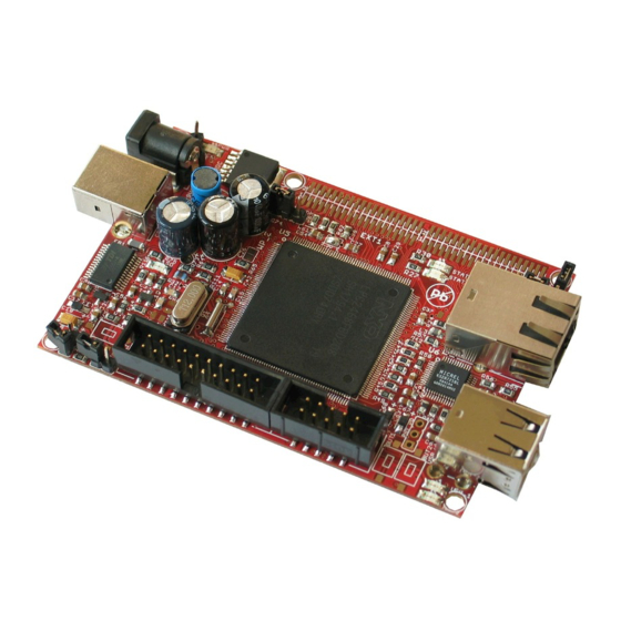
INTRODUCTION: LPC-E2468 uC Linux development prototype board with LPC2468 USB, Ethernet, SD/MMC in credit card format. BOARD FEATURES: MCU: LPC2468; 16MB SDRAM; 128 MB NAN Flash; standard JTAG connector with 2x10 layout programming/debugging with ARM-JTAG; Ethernet 100MBit; 2x USB hosts;... -
Page 3: Board Use Requirements
Software: The board is delivered with uC Linux pre-loaded. You could develop projects for the board with Eclipse, IAR, etc. Please, refer to the LPC-E2468 Quickstart Guide which is on the CD for more details on the software requirements. PROCESSOR FEATURES: The LPC2468 processor has the following features: ●... - Page 4 Four UARTs with fractional baud rate generation, one with ▬ modem control I/O, one with IrDA support, all with FIFO. CAN controller with two channels. ▬ SPI controller. ▬ Two SSP controllers, with FIFO and multi-protocol capabilities. ▬ One is an alternate for the SPI port, sharing its interrupt. SSPs can be used with the GPDMA controller.
- Page 5 ● On-chip power-on reset. On-chip crystal oscillator with an operating range of 1 MHz to 24 MHz. ● 4 MHz internal RC oscillator trimmed to 1 % accuracy that can optionally be used as the system clock. When used as the CPU clock, does not allow CAN and USB to run.
-
Page 6: Block Diagram
BLOCK DIAGRAM:... -
Page 7: Memory Map
MEMORY MAP: LPC2468 memory map... - Page 8 SCHEMATIC:...
-
Page 9: Board Layout
2MB SRAM and the RTC. The board power consumption is: about 150 mA at 9VDC. RESET CIRCUIT: LPC-E2468 reset circuit is made with RC group R4 – 47K, C20 – 100nF and RESET button. CLOCK CIRCUIT: Quartz crystal 12MHz is connected to LPC2468 pin 44 (XTAL1) and pin 46 (XTAL2). -
Page 10: Jumper Description
JUMPER DESCRIPTION: 3.3V_E This jumper, when closed, supplies 3.3 V voltage to the VDD1-10 pins of the MCU. Default state is closed. 3.3VA_E This jumper, when closed, supplies 3.3 V voltage to the VDDA pin of the MCU. Default state is closed. VREF_E This jumper, when closed, supplies 3.3 V reference voltage to the VREF pin... - Page 11 BDS_E Boundary scan enable. Default state is open. BAT/EXT This jumper controls the input power supply for the VBAT pin. If 1-2 are shorted, the external battery is connected to VBAT pin. If 2-3 are shorted, the VBAT pin is supplied by the board +3.3V supply.
- Page 12 INPUT/OUTPUT: One reset button with name RESET – connected to LPC2468 pin 35 (#RESET). Two user buttons with names BUT1 – connected to LPC2468 pin 102 (P2[13]/#EINT3/MCIDAT3/I2STX_SDA) and BUT2 – connected to LPC2468 pin 81 (P2[21]/#DYCS1); Two LEDs named STAT1(green) and STAT2(red) – connected to LPC2468 pin 104 (P4[17]/A17) and LPC2468 pin101 (P4[16]/A16);...
-
Page 13: External Connector Description
EXTERNAL CONNECTOR DESCRIPTION: PWR: Pin # Signal Name You should apply voltage +(9-12)VDC or (6-9) VAC at the PWR pin. USB_D: Pin # Signal Name USBDM USBDP USBDM, USBDP These signals form the differential input/output for the USB device depending on the direction of the data flow. USB_H: Pin # Signal Name Pin # Signal Name... - Page 14 USB_PWRD2 Output USB Power 2. This signal is output from the processor and input for the USB host 2. U2D-, U2D+ This signals form the differential input/output for USB host 2 depending on the direction of the data transfer. JTAG: Signal Name Pin # Signal Name Pin # 3.3V...
- Page 15 TXD1 OutputTransmit Data. This is the asynchronous serial data output (RS232) for the RS232 interface. RXD1 Input Receive Data. This is the asynchronous serial data input (RS232) for the RS232 interface. SCL0 Serial (Synchronization) Clock. This is the synchronization clock for the data transfer through I2C interface.
- Page 16 SD/MMC card slot: Pin # Signal Name Pin # Signal Name MCIDAT3 MCICMD GND (VSS1) MCICLK GND (VSS2) MCIDAT0 MCIDAT1 MCIDAT2 MCIDAT0-3 I/O Memory Card Interface Data 0-4. These are the data lines for the SD/MMC connector. They could be both input and output for the MCU depending on the data flow direction.
- Page 17 EXT1&EXT2: Pin # Signal Pin # Signal Pin # Signal Pin # Signal Name Name Name Name EXT1-1 3.3V EXT1-2 EXT2-1 3.3V EXT2-2 EXT1-3 EXT1-4 RSTN EXT2-3 EXT2-4 P4[23] EXT1-5 ALARM EXT1-6 P1[29] EXT2-5 P4[22] EXT2-6 P4[21] EXT1-7 P1[28] EXT1-8 P1[26] EXT2-7 P4[20]...
-
Page 18: Mechanical Dimensions
MECHANICAL DIMENSIONS: All measures are in mm. AVAILABLE DEMO SOFTWARE: LPC-E2468 is delivered pre-loaded with C Linux and the sources and binaries are on the accompanying CD. -
Page 19: Order Code
This document is intended only to assist the reader in the use of the product. OLIMEX Ltd. shall not be liable for any loss or damage arising from the use of any information in this document or any error or omission in such...
Need help?
Do you have a question about the LPC-E2468 and is the answer not in the manual?
Questions and answers