Table of Contents
Advertisement
Quick Links
SERVICE MANUAL
SERVICE MANUAL
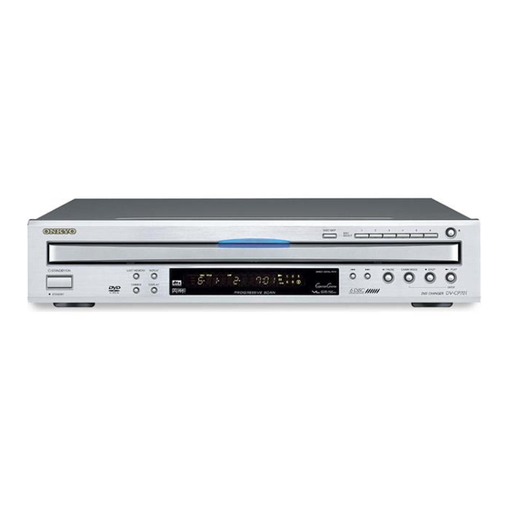
DVD CHANGER
DV-CP701
MODEL
Black and Silver models
B MDD, S MDD
120V AC, 60Hz
B MPA
220-230V AC, 50/60Hz
SAFETY-RELATED COMPONENT
WARNING!!
COMPONENTS IDENTIFIED BY MARK
SCHEMATIC DIAGRAM AND IN THE PARTS LIST ARE
CRITICAL FOR RISK OF FIRE AND ELECTRIC SHOCK.
REPLACE THESE COMPONENTS WITH ONKYO
PARTS WHOSE PART NUMBERS APPEAR AS SHOWN
IN THIS MANUAL.
MAKE LEAKAGE-CURRENT OR RESISTANCE
MEASUREMENTS TO DETERMINE THAT EXPOSED
PARTS ARE ACCEPTABLY INSULATED FROM THE
SUPPLY CIRCUIT BEFORE RETURNING THE
APPLIANCE TO THE CUSTOMER.
Ref. No. 3760
ON
STANDBY
SEARCH LAST M MEMORY CHAIN MODE
1
4
7
+10
TOP MENU
RETURN
AUDIO
ANGLE SUBTITLE
DISC 1
DISC 2
DISC 4
DISC 5
DISC SKIP
PROGRESSIVE
RC-542DV
ON THE
DV-CP701
052003
OPEN/
CLOSE
REPEAT
2
3
A-B
5
6
RANDOM
8
9
DISPLAY
0
CLEAR
MENU
ENTER
SETUP
ZOOM
DISC 3
STEP/SLOW
DISC 6
DIMMER
RC-542DV
Advertisement
Table of Contents

Related Manuals for Onkyo DV-CP701


Summary of Contents for Onkyo DV-CP701
- Page 1 COMPONENTS IDENTIFIED BY MARK ON THE SCHEMATIC DIAGRAM AND IN THE PARTS LIST ARE CRITICAL FOR RISK OF FIRE AND ELECTRIC SHOCK. REPLACE THESE COMPONENTS WITH ONKYO PARTS WHOSE PART NUMBERS APPEAR AS SHOWN IN THIS MANUAL. MAKE LEAKAGE-CURRENT OR RESISTANCE...
-
Page 2: Specifications
DV-CP701 SPECIFICATIONS Video system Standard NTSC (U.S. model), PAL/AUTO (Australian model) Region code 1 (U.S. model), 4 (Australian model) Laser Semiconductor laser, wavelength 650 nm (DVD), 780 nm (CD) 4 Hz-22 kHz @ 48 kHz sampling rate DVD linear audio... -
Page 3: Laser Warning
DV-CP701 SERVICE PROCEDURES-1 PROTECTION OF EYES FROM LASER BEAM DURING SERVICING This set employs a laser. Therefore, be sure to follow carefully the instructions below when servicing. Laser Diode Properties WARNING!! Wavelength: 650/780nm (DVD/CD) SERVICE WARNING : DO NOT APPROACH THE LASER EXIT WITH THE EYE TOO CLOSELY. -
Page 4: Service Procedures
DV-CP701 SERVICE PROCEDURES-2 2. Safety-check out (Only U.S.A. model) After correcting the original service problem perform the following safety check before releasing the set to the customer Connect the insulating-resistance tester between the plug of power supply cord and terminal GND on the back panel. - Page 5 DV-CP701 A215 A215 A215 A215 A215 A214 A215 (U6) (U7) P707 (U9) (U12) (U8) Cloth tape (80) <S> only...
-
Page 6: Exploded View
EXPLODED VIEW P702 (U3) Cloth tape (80) P1101 P1001 Cloth tape (160) P2001 Cloth tape P901 P2401 P2501 P2901 F001 E821 E102... - Page 7 DV-CP701 EXPLODED VIEW A215 A215 P702 A215 A215 (U3) Cloth tape (80) P1101 A215 P1001 A214 A215 Cloth tape (160) P2001 Cloth tape P901 P2401 P2501 P2901 (U6) (U7) P707 F001 (U9) (U12) (U8) Cloth tape (80) E821 <S> only...
- Page 8 DV-CP701 BLOCK DIAGRAM P2001A Q109:DTA114YKA P1001 NAAF-7811 DACCLK,LRCLK,BCLK,DATAD,DOUT0-1 Q110:DTC114YKA LASER etc MD,MC,CSDACD,DACRST Q403(2/2) Q401 Q403(1/2) Q109,Q110 DVD MECHA Q405 P1101 PCM1742KE FILTER CCT VLSC MUTING AUDIO OUT SPD+,SPD-,SLD+,SLD,LMT-SW P702B Q404(2/2) AUDIO DAC Q404(1/2) Q407,Q408 RI,RESET,AMUTE NADG-7807 Q406 DVD MAIN CIRCUIT PC BOARD...
-
Page 9: Block Diagram
BLOCK DIAGRAM P1001 LASER etc DVD MECHA P1101 SPD+,SPD-,SLD+,SLD,LMT-SW NADG-7807 DVD MAIN CIRCUIT PC BOARD P2901 P2501 POWER SUPPLY UNIT EV5V SW5V P 9 0 1 NGPS-0036 (US) SW3.3V P 7 1 0 A SW8V NGPS-0037( AUS) A+12V EV5V,SW5V,SW3. A-12V -30V SUBRST,SUBCL,SUBREQ,SUBSI,SUB NADIS-7808... - Page 10 DV-CP701 P2001A Q109:DTA114YKA NAAF-7811 DACCLK,LRCLK,BCLK,DATAD,DOUT0-1 Q110:DTC114YKA MD,MC,CSDACD,DACRST Q403(2/2) Q401 Q403(1/2) Q109,Q110 Q405 PCM1742KE FILTER CCT VLSC MUTING AUDIO OUT P702B Q404(2/2) AUDIO DAC Q404(1/2) Q407,Q408 RI,RESET,AMUTE Q406 Q403-Q406:NJM4580M-D Q407,Q408:HN1C03F DIG OUT P403A NAVD-7810 Q201 LA73054 COMPONENT P 2 4 0 1 A...
- Page 11 DV-CP701 IN CIRCUIT PC BOARD-1 (F/E SECTION) NADG-7807 NADG-7807 RFAC AMPSEN AMPSDT AMPSCK DFCT MIRR C2PO DADT LRCK DOUT R1224 R1225 DRVRDY DRVTX DRVIRQ DRVCLK DRVRX R1226 R1227 DRVRST DRVRST VDT7 DRVRX P100 VDT6 DRVCLK P101 VDT5 DRVIRQ P102 VDT4...
-
Page 12: Schematic Diagram
SCHEMATIC U1 : DVD MAIN A3.3V Q1004 R1004 CD/XDVD RFAC0 RFAC Q1003 DIAGRAM 2SK3019 CD/XDVD Q1005 C1032 22/16 104K C1029 C1028 2SK3019 C1031 104Z 104K 2SK3019 AGND RFOP AMPSEN AMPSDT RF-OP RF-OP AMPSEN VC25 AMPSDT AMPSCK C1001 104K RFSIN C1002 104K C1003 220J AGND C1004 220J... - Page 13 DV-CP701 SCHEMATIC U1 : DVD MAIN CIRCUIT PC BOARD-1 (F/E SECTION) NADG-7807 A3.3V Q1004 R1004 CD/XDVD RFAC0 RFAC Q1003 DIAGRAM 2SK3019 Q1005 CD/XDVD C1032 22/16 104K C1029 NADG-7807 RFAC C1028 2SK3019 C1031 104Z 104K 2SK3019 AGND RFOP AMPSEN AMPSDT RF-OP...
- Page 14 DV-CP701 MINAL PC BOARD AGND A3.3V P2001B DGND D3.3V AGND A1.8V DGND D1.8V C2901 100/6.3 MPC2918T Q2902 L2903 PGND 2.2U MPC29M33T Q2901 L2902 PGND 2.2U SW+5V DGND R2901 SW+3.3V R2902 DGND1 R2903 SW+3.3V MPC2918T SW+1.8V Q2903 BED+3.3V L2002 2.2U BED+1.8V L2001 2.2U...
- Page 15 SCHEMATIC U1 : DVD MAIN CIRCUIT PC BOARD-2 (B/E SECTION) NADG-7807 DIAGRAM To AUDIO OUTPUT TERMINAL NAAF-7811 P2002B DRVIRQ DRVRDY DRVCLK DRVRX DRVTX DRVRST DOUT LRCK DADT HDRQ XHAC R2054 XSHD VDT7 BED+3.3V VDT6 BED+1.8V VDT5 VCC 14 VDT4 4G 13 VDT3 4A 12 VDT2...
- Page 16 DV-CP701 SCHEMATIC U1 : DVD MAIN CIRCUIT PC BOARD-2 (B/E SECTION) NADG-7807 DIAGRAM To AUDIO OUTPUT TERMINAL PC BOARD NAAF-7811 AGND A3.3V P2002B P2001B DGND D3.3V AGND A1.8V DGND DRVIRQ D1.8V C2901 100/6.3 DRVRDY MPC2918T DRVCLK Q2902 L2903 DRVRX PGND DRVTX 2.2U...
- Page 17 DV-CP701 U3 : MECHANISM CONTROL CIRCUIT PC BOARD NADG-7809 UDZS5.1B 200mS Delay Q702 D733 1SS352 D734 VOUT R747 R748 AMUTE/UCOM 1SS352 R746 VDOFF S-80145 D731 1SS352 IRIN IRIN P64/GND R752 P/OFF P63/GND DSTBX P62/GND SUB_RDY P61/GND P04/GND P60/GND P05/GND P57/NC...
- Page 18 SCHEMATIC DIAGRAM P706 WRITE IN FLASH PLUG NCETC-7896 U12 : DISC SENSOR PC BOARD P706B NAETC-7818 P706A Q710 DISC SENSOR DTC114YKA Q709 R701 Q716 8.2K DTC114YKA GP2S28 R703 STOP_POSITION SENSOR Q711 DTC114YKA Q712 Q717 R705 8.2K DTC114YKA RPI-576 R707 R767 ROULETTE MOTOR DRIVE Q704 TA7291S...
- Page 19 DV-CP701 PRINTED CIRCUIT BOARD VIEW FROM COMPONENT SIDE VIEW (U3) : MECHANISM CONTROL PC BOARD (NADG-7809) J751 P701A P710A P702A J734 P711A J733 C719 J732 C721 J763 J737 J717 C717 J738 J711 C713 C715 J739 SW3.3 SW3.3 J716 SW5VGND SW5VGND...
- Page 20 DV-CP701 SCHEMATIC DIAGRAM U2 : DISPLAY CIRCUIT PC BOARD NADIS-7808 NADIS-7808 Q802 HNV-12SM34 P23 40 P24 39 P25 38 P26 37 P27 36 P28 35 P29 34 Q801 P30 33 P31 32 R838 U6 : DISC SELECT SWITCH PC BOARD NASW-7812...
-
Page 21: Naetc
SCHEMATIC DIAGRAM U2 : DISPLAY CIRCUIT PC BOARD NADIS-7808 NADIS-7808 Q802 HNV-12SM34 P23 40 P24 39 P25 38 P26 37 P27 36 P28 35 P29 34 Q801 P30 33 P31 32 MPD780232GC-070-8BT P32 31 P33 30 P34 29 P35 28 JOGB 27 JOGA 26 VDD 25... - Page 22 DV-CP701 R838 U6 : DISC SELECT SWITCH PC BOARD NASW-7812 100K R837 R836 100K R835 100K 100K R801 R802 R803 R804 R805 R806 R807 1.8K 3.9K R834 2.7K R833 2.7K R832 2.7K R847 R831 D802 R848 2.7K SLR-343BBT Q810 R849...
- Page 23 DV-CP701 SCHEMATIC DIAGRAM U4 : VIDEO SIGNAL OUTPUT TERMINAL PC BOARD (NAVD-7810) VIDEO/OFF L221 C231 R282 GAIN6DB 220UH Q201 R208 R281 C201 104K NCH-1482 LA73054 GAIN9DB R209 VCC1 AMP1.S 36 R211 R216 CV.IN DRIVE1 35 1_DRIVE SQEZ SQEZ SQUEEZE VCC3 34 C212 1000/6.3...
- Page 24 SCHEMATIC DIAGRAM U4 : VIDEO SIGNAL OUTPUT TERMINAL PC BOARD (NAVD-7810) VIDEO/OFF L221 C231 R282 220UH R281 NCH-1482 C201 104K SQEZ SQEZ LTTR LTTR C202 CR/R C203 CB/B 10/16 YC/C VIDEO/OFF SW+5V C205 10/16 C207 10/16 CR/R VGND CB/B C209 VGND 10/16 YC/G...
- Page 25 DV-CP701 GAIN6DB Q201 R208 LA73054 GAIN9DB R209 VCC1 AMP1.S 36 R211 R216 CV.IN DRIVE1 35 1_DRIVE SQUEEZE VCC3 34 C212 1000/6.3 R215 L201 LETTER CV.O 33 R210 R217 BK1608LM182-T MUTE1 GND8 32 L202 2_DRIVE R218 C.IN C.OUT 31 R212 BK1608LM182-T...
- Page 26 DV-CP701 SCHEMATIC DIAGRAM U14: POWER SUPPLY UNIT (NGPS-0036-100-120V <MDD>) (NGPS-0037-100-240V <MPA>) EV+12V P-con SJW1 SW+8V C30 R32 SW+8V C30: Open <MDD>, 102K <Other> R27: Open <MDD>, AC-H AC-G 8.2 ohm <Other> AC INPUT 15.16 SW+5V PHC1 R27 C11 C11: Open <MDD>, 102K <Other>...
-
Page 27: Wiring View
DV-CP701 WIRING VIEW AC IN P1292 P1291 P202A P202B Q412 SPD+ P301 SPD- P201 P402 SLD+ SLD- LMT-SW P201 DACRST DGND P202B AMUTE CSDMIX DGND1 DACCLK DGND1 U4: Video signal output terminal PC board D-DMIX LRCK BCTCLK NAVD-7810 DGND1 DOUT1... -
Page 28: Printed Circuit Board View
DV-CP701 PRINTED CIRCUIT BOARD VIEW : DVD MAIN CIRCUIT PC BOARD (NADG-7807) : Side A pattern : Sise B pattern... - Page 29 DV-CP701 PRINTED CIRCUIT BOARD VIEW : DVD MAIN CIRCUIT PC BOARD (NADVG-7807)
- Page 30 DV-CP701 PRINTED CIRCUIT BOARD VIEW FROM COMPONENT SIDE VIEW (U3) : MECHANISM CONTROL PC BOARD (NADG-7809) J751 P701A P710A P702A J734 P711A J733 C719 J732 C721 J763 J737 J717 C717 J738 J711 C713 C715 J739 SW3.3 SW3.3 J716 SW5VGND SW5VGND...
- Page 31 DV-CP701 PRINTED CIRCUIT BOARD VIEW FROM SOLDERING SIDE : DISPLAY CIRCUIT PC BOARD (NADIS-7807) P704 ANGLE_TYPE/DV-CP701 J803 J805 R846 J804 J812 NCDIS-7808 25137808A J802 J806 C804 Q802 Q808 Q802 Component side C813 C814 Q801 C818 Q805 R856 Q801 Q806 C803...
-
Page 32: Naaf
DV-CP701 PRINTED CIRCUIT BOARD VIEW FROM BOTTOM SIDE : AUDIO SIGNAL OUTPUT TERMINAL PC BOARD (NAAF-7811) NCAF-7811 25137811 C407 C405 AMUTE/M DACRST J426 CSDMIX DGND J420 DACCLK DAT-DMIX BITCLK C420 DIG1 J421 A-12V C402 C419 AGND C406 J414 A+12V C408 SW3.3V... - Page 33 DV-CP701 PRINTED CIRCUIT BOARD VIEW FROM SOLDERING SIDE (U6) : DISC SELECT SWITCH PC BOARD (NASW-7812) P802A DISC3 DISC4 DV-CP701 DISC1 DISC2 OPEN/CLOSE DISC/SKIP DISC5 DISC6 25137812 NCSW-7812 Component side view R807 R801 R802 R804 R806 R805 R803 Soldering side view...
- Page 34 DV-CP701 PRINTED CIRCUIT BOARD VIEW FROM SOLDERING SIDE (U12) : DISC SENSOR PC BOARD (NAETC-7818) NCETC-7818 25137818 R761 R764 P707B C764 C762 R763 C763 Q717 Component side view Soldering side view (U11) : LOADING MOTOR PC BOARD (NAETC-7817) C766 Z702...
-
Page 35: Navd
DV-CP701 PRINTED CIRCUIT BOARD VIEW FROM SOLDERING SIDE (U4) : VIDEO SIGNAL OUTPUT TERMINAL PC BOARD (NAVD-7810) P2401A J209 J202 J205 J201 J210 J206 P701B J207 J211 J208 P701B J212 J204 C211 J215 C210 J216 J213 J217 J214 J219 J220... -
Page 36: Pin Definition
DV-CP701 IC BLOCK DIAGRAM/ TERMINAL DESCRIPTION Q1101: FAN8042 5-CH MOTOR DRIVER-1 PIN ASSIGNMENT PIN DEFINITION Pin Number Pin Name Pin Function description IN1+ CH1 op-amp input (+) IN1- CH1 op-amp input (-) OUT1 CH1 op-amp output IN1+ DO1+ IN2+ CH2 op-amp input (+) - Page 37 DV-CP701 IC BLOCK DIAGRAM/ TERMINAL DESCRIPTION Q1101: FAN8042 5-CH MOTOR DRIVER-2 OP-AMP OP-AMP POWER IN1+ DO1+ SAVE IN1- DO1- OUT1 DO2+ IN2+ DO2- IN2- DO3+ OUT2 DO3- IN3+ Input DO4+ op-amp IN3- DO4- OUT3 DO5+ IN4+ MUTE123 MUTE4 TSD-M DO5-...
- Page 38 DV-CP701 IC BLOCK DIAGRAM/ TERMINAL DESCRIPTION Q2502: TC7SZ125FU (BUS BUFFER 3-STAGE OUTPUT) PIN ASSIGNMENT IN A Truth table INPUT OUTPUT OUT Y (Top view) X: Don't care Z: High impedance...
- Page 39 DV-CP701 IC BLOCK DIAGRAM / TERMINAL DESCRIPTION Q411 : TC74VHCU04FT Hex inverter Pin layout 14 Vcc 13 6A 12 6Y 11 5A Truth table 10 5Y 9 4A 8 4Y...
- Page 40 DV-CP701 IC BLOCK DIAGRAM/ TERMINAL DESCRIPTION Q2501: TC74VHCT125AF QUAD BUS BUFFER Pin Assignment Truth Table INPUTS OUTPUTS X: Don't Care Z: High Impedance...
-
Page 41: System Diagram
DV-CP701 IC BLOCK DIAGRAM/ TERMINAL DESCRIPTION Q2301: TC74VCX162373FT 16-BIT D-TYPE LATCH PIN ASSIGNMENT Truth Table Inputs Outputs 1D1-1D8 1Q1-1Q8 SYSTEM DIAGRAM Inputs Outputs 2D1-2D8 2Q1-2Q8 LE Q LE Q LE Q LE Q LE Q LE Q LE Q LE Q... - Page 42 DV-CP701 IC BLOCK DIAGRAM/ TERMINAL DESCRIPTION Q704, Q705: TA7291S (MOTOR DRIVER) Vcc Vref Reg. Power Supply INPUT OUTPUT OUT1 MODE OUT1 OUT2 STOP OUT2 CW/CCW Protection CCW/CW circuit BRAKE CW: Clockwise direction CCW: Counter clockwise direction IN1 IN2...
-
Page 43: Pin Configuration
DV-CP701 IC BLOCK DIAGRAM/ TERMINAL DESCRIPTION Q2002: S-80127CNMC-JKM VOLTAGE DETECTOR (12.7V N-ch open drain, Active L: out) Q702: S-80130CLMC-JKM VOLTAGE DETECTOR (13.0V CMOS, Active L: out) PIN CONFIGURATION PIN DESCRIPTION Symbol Description ON/OFF switch for delay time Top view Non-connection... -
Page 44: Pin Assignments
DV-CP701 IC BLOCK DIAGRAM/ TERMINAL DESCRIPTION Q401: PCM1742KE DIGITAL-TO-ANALOG CONVERTER 24-Bit, 192kHz Sampling Enhanced Multilevel, Delta-Sigma, Audio BLOCK DIAGRAM Audio LRCK Output Amp and Serial Port Low-Pass Filter 4x/8x DATA Enhanced Over sampling Multilevel Digital Filter Delta-Sigma with Modulator Function... -
Page 45: Exploded View Parts List
EXPLODED VIEW PARTS LIST !: Safety part REF. NO. PART NAME DESCRIPTION PART NO. Front Panel <B> 1466-1801-0 Front Panel 1466-1802-0 <S> KNOB (STBY) 2446-3901-0 <B> KNOB (STBY) <S> 2446-3701-0 KNOB (SEL) <B> 2446-4101-0 KNOB (SEL) <S> 2446-3801-0 KNOB (EJECT) 2446-4601-0 <B>... -
Page 46: Packing Parts List
P707 NCFC6-063012 7012-6522-0 P901 Power cord 253333VOL AS-UC-2 <MDD> P901 or Power cord AS-UC-2 <MDD> 253332HIT P901 Power cord AS-SAA <MPA> 253197HIT P901 or Power cord AS-SAA <MPA> 253307VOL GPE P/N DVD Main circuit PC board assy NADG-7807A-1A <MDD, MPA> 1H498507-1A SVC-7807-1A Display circuit PC board assy SVC-Q0090C-1A... - Page 47 E804 S- Cable (S CORD) 2010380 E804 or S- Cable TPX3000 2010360 E805 Remote Controller RC-542DV 8912-0036-0 24140542 E810 Instruction Manual E (DVCP701) 4301-7046-0 29343461A <B>: Black color model <S>: Silver color model <MDD>: North American and Canadian area only <MPA>: Australian area only...
- Page 48 CHANGER MECHANISM PARTS LIST REF. No. PART NAME DESCRIPTION PART No. Rail 4154-6031-0 24840157A Loading motor assy M002+M003 Q0090C-MOTCC Tapping screw 3TTB+8B 838130088 Screw 2.6TTP+4S 833126047 Rubber Belt DVCP701 4157-0281-0 Gear (PULLEY) 4154-6061-0 Gear 4154-6091-0 Gear (MAIN) 4154-6071-0 248100087A Gear (CAM) 4154-6101-0 Screw...
- Page 49 PRINTED CIRCUIT BOARD PARTS LIST U1: DVD MAIN CIRCUIT PC BOARD (NADG-7807) 1/8 PAGE CIRCUIT NO. PART NO. DESCRIPTION REMARK Q1001 3131-9990-0 CXD1881BR 22241902R3 Q1002 22241676R2 NJM2115V Q1101 3132-0020-0 FAN8042 22241905R3 Q1102 3132-0030-0 BA4510FV 22241907R2 Q1201 3132-0040-0 CXD1885Q 22241903R3 Q1251 3132-0050-0 IC41LV16100-50T, EDO-DRAM 22241909R2...
- Page 50 C2403 356721019R2 CEWX6.3V-100M C2415 356741009R2 CEWX16V-10M 2/8 PAGE C2418 356721019R2 CEWX6.3V-100M C2601 356722209R2 CEWX6.3V-22M C2602 356721019R2 CEWX6.3V-100M C2901 356721019R2 CEWX6.3V-100M C2902 356721019R2 CEWX6.3V-100M C2903 356721019R2 CEWX6.3V-100M C2904 356721019R2 CEWX6.3V-100M C2905 356721019R2 CEWX6.3V-100M C2907 3567A2219R2 CEWX4V-220M C2906 356721019R2 CEWX6.3V-100M Coils L1001 231237K470R2 NCH-1479 L1002...
- Page 51 R1237 43474410104R1 RM4KJ101X04 R1238 43474410104R1 RM4KJ101X04 3/8 PAGE R1241 43474410104R1 RM4KJ101X04 R1251 43474410104R1 RM4KJ101X04 R1252 43474410104R1 RM4KJ101X04 R1253 43474410104R1 RM4KJ101X04 R1254 43474410104R1 RM4KJ101X04 R1291 8911-0020-0 RM6KJ103X08 43474610308R1 R1292 8911-0020-0 RM6KJ103X08 43474610308R1 R1293 8911-0020-0 RM6KJ103X08 43474610308R1 R2022 43474447004R1 RM4KJ470X04 R2023 43474447004R1 RM4KJ470X04 R2025 43474447004R1...
-
Page 52: U4 : Video Signal Output Terminal Pc Board (Navd
Q707 2214373R2 2SA1162-O Q708 or 2216260R2 RN1407 4/8 PAGE Q708 or 2216340R2 KRC107S Q709 2216470R2 DTC114YKA Q709 or 2216260R2 RN1407 Q709 or 2216340R2 KRC107S Q710 2213145R2 2SC2712-GR Q711 2213145R2 2SC2712-GR Q712 2216470R2 DTC114YKA Q712 or 2216260R2 RN1407 Q712 or 2216340R2 KRC107S Q713 2211705... -
Page 53: Naaf
CIRCUIT NO. PART NO. DESCRIPTION REMARK 5/8 PAGE Q201 22241767R2 LA73054 Q411 22274004HR2TO TC74VHCU04FT Transistors Q202 2216470R2 DTC114YKA Q202 or 2216260R2 RN1407 Q202 or 2216340R2 KRC107S Q203 2216480R2 DTA114YKA Q203 or 2216360R2 RN2407 Q203 or 2216350R2 KRA107S Coils L201 230958R1 BK1608LM182-T, EMI Filter L202 230958R1... - Page 54 Q408 2216141R2 HN1C03F-B Coils 6/8 PAGE L403 231237M022R2 NCH-1471, Choke L406 231237M022R2 NCH-1471, Choke L407 230958R1 BK1608LM182-T, EMI Filter Diodes D101 223269R2 1SS355 D101 or 223234R2 1SS352 D102 223269R2 1SS355 D102 or 223234R2 1SS352 D103 223269R2 1SS355 D103 or 223234R2 1SS352 D104 223269R2...
- Page 55 P806A 7012-6549-0 NSAS-6P1137 200EE340615UL Push switch 7/8 PAGE S801 25035718 NPS-111-S681 S802 25035718 NPS-111-S681 S803 25035718 NPS-111-S681 S804 25035718 NPS-111-S681 S805 25035718 NPS-111-S681 S806 25035718 NPS-111-S681 S807 25035718 NPS-111-S681 S808 25035718 NPS-111-S681 U7: KEY OPERATION SWITCH PC BOARD (NASW-7813) CIRCUIT NO. PART NO.
- Page 56 Sockets P707B 25052239 NSCT-6P2136 8/8 PAGE P707Bor 25052052 NSCT-6P1839 P707Bor 25051850 NSCT-6P1637 Photo interrupter Q716 24190046 GP2S28, Disc sensor Photo coupler Q717 481P-I576-3 RPI-576, Disc stop sens. 24120107...
- Page 57 DV-CP701 IC BLOCK DIAGRAM/ TERMINAL DESCRIPTION Q403,Q404,Q405,Q406 NJM4580M-D (2-ch Ope. amp.) Pin description 1. A OUTPUT 2. A -INPUT 3. A +INPUT 4. V- 5. B +INPUT 6. B -INPUT 7. B OUTPUT 8. V+ (Top view)
- Page 58 DV-CP701 IC BLOCK DIAGRAM/ TERMINAL DESCRIPTION Q2401: NJM2373AF (Adjustable High Precision Shunt Regulator) Pin Configuration Block Diagram Cathode REFERENCE Reference ANODE CATHODE Anode...
- Page 59 DV-CP701 IC BLOCK DIAGRAM/ TERMINAL DESCRIPTION Q431: NJM2370 (Regulated power supply) CONT Thermal Protection NOISE PIN DESCRIPTION BYPASS 1. Control 2. GND 3. Noise Bypass Band gap Reference 4. Vout 5. Vin...
- Page 60 DV-CP701 IC BLOCK DIAGRAM/ TERMINAL DESCRIPTION Q1002: NJM2115V (2-ch Ope. amp.) Pin description 1. A OUTPUT 2. A -INPUT 3. A +INPUT 4. V- 5. B +INPUT 6. B -INPUT 7. B OUTPUT 8. V+ (Top view)
- Page 61 DV-CP701 IC BLOCK DIAGRAM/ TERMINAL DESCRIPTION Q201 : LA73054 6-CHANNEL VIDEO DRIVER Block Diagram AMP1 3 SW CC +5V (9dB/6dB) COMPOSITE IN CLAMP 2 Drive/1 Drive SQUEEZE SW 2 Step Amp 1 C_OFFSET CC +5V DC_CTL LETTER BOX SW COMPOSITE...
- Page 62 DV-CP701 IC BLOCK DIAGRAM/ TERMINAL DESCRIPTION Q2003 : IS24C08-3Z EEPROM (8K-Bit 2-Wire Serial CMOS EEPROM) PIN CONFIGURATION PIN DESCRIPTIONS A0-A2 Address Inputs Serial Address/Data I/O Serial Clock Input Write Protect Input Power Supply Ground This input clock pin is used to synchronize the data transfer to and from the device.
-
Page 63: Pin Configurations
DV-CP701 IC BLOCK DIAGRAM/ TERMINAL DESCRIPTION Q2303 : IC42S16400-7T SYNCHRONOUS DYNAMIC RAM The IC42S16400 are high-speed 67, 108, 864-bit synchronous dynamic ramdam-access memories, organized as 2,097, 152 x 8 x 4 and 1,48, 576 x 16 x 4 (word x bit x bank), respectively. -
Page 64: Truth Table
DV-CP701 IC BLOCK DIAGRAM/ TERMINAL DESCRIPTION Q1251: IC41LV16100-50T 16-MBIT DYNAMIC RAM PIN CONFIGURATION FUNCTIONAL BLOCK DIAGRAM I/O0 1/O15 1/O1 1/O14 LCAS 1/O2 1/O13 CLOCK CONTROL CONTROL 1/O3 1/O12 UCAS GENERATOR LOGICS LOGICS 1/O4 1/O11 1/O5 1/O10 1/O6 1/O9 1/O7 1/O8... - Page 65 DV-CP701 IC BLOCK DIAGRAM/ TERMINAL DESCRIPTION Q2901, Q2904 : uPC29M33T REGURATOR IC 3.3 V output Q2902, Q2903 : uPC2918T REGURATOR IC 1.8 V output BLOCK DIAGRAM INPUT Sate operating area protection Reference Start-up voltage Saturation circuit Drive Error protection OUTPUT circuit amp.
-
Page 66: Pin Layout
DV-CP701 MICROPROCESSOR TERMINAL DESCRIPTION PIN LAYOUT RESET RESET 60 P15/ANI5 P127/RTP7 59 P16/ANI6 MCRST P126/RTP6 58 P17/ANI7 AVSS RIOUT P125/RTP5 57 Avss RIIN P124/RTP4 56 P130/ANO0 FL ON/OFF P123/RTP3 55 P131/ANO1 AVREF1 P122/RTP2 54 AVREF1 FPSI P121/RTP1 53 P70/SI2/RxD0 FLSO... - Page 67 DV-CP701 MICROPROCESSOR TERMINAL DESCRIPTION-1 Sign Functional name I/O Description P15/ANI5 P16/ANI6 P17/ANI7 MCRST O Reset output pin for sub microprocessor. Avss AVSS I To connect VSS. P130/ANO0 P131/ANO1 FL ON/OFF O Power ON/ OFF pin of FL tube. AVREF1 AVREF1 I Reference voltage input pin for D/A converter.
- Page 68 DV-CP701 MICROPROCESSOR TERMINAL DESCRIPTION-2 Sign Functional name Description P64/RD Not used. To connect to GND P65/WR Not used. To connect to GND P66/WAIT Not used. To connect to GND P67/ASTB Not used. To connect to GND P30/TO0 VDOFF O Video off signal output pin.
-
Page 69: Part Replacement
DV-CP701 PART REPLACEMENT-1 1. CABINET REPLACEMENT 1-3. Tray panel and Mechanism assy <Mechanism assy> 1-1. Top cover and front panel 1-3-1. Remove four screws. (1) 1-1-1. Remove the top cover. (six screws) 1-3-2. Remove the mechanism assy. 1-1-2. Remove the front panel assy. Remove the FFC (P704) and 1-3-3. - Page 70 DV-CP701 PART REPLACEMENT-2 Tray panel <Mounting> 1-4-4. Insert the tray panel. 1-4-5. Set the FFC (P707) to mechanism control PC board assy. 1-4-6. The pin of main gear and fiting the position of the slot on the tray. 1-4-7. Pull up the nail on the tray panel and insert the tray.
- Page 71 DV-CP701 UPGRADE THE FIRMWARE/ TEST MODES 1 Updating the Firm Ware 1-1 Open the DISC tray and set the Firm Ware Recorded DISC on DISC1 bay. 1-2 Close the DISC tray. Will start the Firm Ware updating automatically. Will tray open after finish the updating.
- Page 72 5-5 Press "STANDBY" key of the DV-CP701 to exit the REGION setting mode. 6 Initialization 6-1 Press the "STOP" & "STANDBY" at the same on the DV-CP701 with NO DISC condition. 6-2 It's display "COMPLETE" on FL tube after initializing for setting and mechanism setting.
- Page 73 DV-CP701 UPGRADE THE FIRMWARE/ TEST MODES MDD1N Default Setting Layer 1 Layer 2 Layer 3 Layer 4 Picture TV Shape 4:3 Letter box Interlaced Setting Progressive Setting Audio Dolby Digital Out Dolby Digital Out Dolby Digital Linear PCM Out Down Sample On...
-
Page 74: Packing View
DV-CP701 PACKING VIEW E801 A652 E810 E805 E804 E802 E803 RC-542DV A604 A608 A701 A606 A602 A610 A603 A651 A655... - Page 75 EXPLODED VIEW PARTS LIST !: Safety part REF. NO. PART NAME DESCRIPTION PART NO. Front Panel <B> 1466-1801-0 Front Panel 1466-1802-0 <S> KNOB (STBY) 2446-3901-0 <B> KNOB (STBY) <S> 2446-3701-0 KNOB (SEL) <B> 2446-4101-0 KNOB (SEL) <S> 2446-3801-0 KNOB (EJECT) 2446-4601-0 <B>...
- Page 76 P707 NCFC6-063012 7012-6522-0 P901 Power cord 253333VOL AS-UC-2 <MDD> P901 or Power cord AS-UC-2 <MDD> 253332HIT P901 Power cord AS-SAA <MPA> 253197HIT P901 or Power cord AS-SAA <MPA> 253307VOL GPE P/N DVD Main circuit PC board assy NADG-7807A-1A <MDD, MPA> 1H498507-1A SVC-7807-1A Display circuit PC board assy SVC-Q0090C-1A...
- Page 77 E804 S- Cable (S CORD) 2010380 E804 or S- Cable TPX3000 2010360 E805 Remote Controller RC-542DV 8912-0036-0 24140542 E810 Instruction Manual E (DVCP701) 4301-7046-0 29343461A <B>: Black color model <S>: Silver color model <MDD>: North American and Canadian area only <MPA>: Australian area only...
- Page 78 CHANGER MECHANISM PARTS LIST REF. No. PART NAME DESCRIPTION PART No. Rail 4154-6031-0 24840157A Loading motor assy M002+M003 Q0090C-MOTCC Tapping screw 3TTB+8B 838130088 Screw 2.6TTP+4S 833126047 Rubber Belt DVCP701 4157-0281-0 Gear (PULLEY) 4154-6061-0 Gear 4154-6091-0 Gear (MAIN) 4154-6071-0 248100087A Gear (CAM) 4154-6101-0 Screw...
- Page 79 PRINTED CIRCUIT BOARD PARTS LIST U1: DVD MAIN CIRCUIT PC BOARD (NADG-7807) 1/8 PAGE CIRCUIT NO. PART NO. DESCRIPTION REMARK Q1001 3131-9990-0 CXD1881BR 22241902R3 Q1002 22241676R2 NJM2115V Q1101 3132-0020-0 FAN8042 22241905R3 Q1102 3132-0030-0 BA4510FV 22241907R2 Q1201 3132-0040-0 CXD1885Q 22241903R3 Q1251 3132-0050-0 IC41LV16100-50T, EDO-DRAM 22241909R2...
- Page 80 C2403 356721019R2 CEWX6.3V-100M C2415 356741009R2 CEWX16V-10M 2/8 PAGE C2418 356721019R2 CEWX6.3V-100M C2601 356722209R2 CEWX6.3V-22M C2602 356721019R2 CEWX6.3V-100M C2901 356721019R2 CEWX6.3V-100M C2902 356721019R2 CEWX6.3V-100M C2903 356721019R2 CEWX6.3V-100M C2904 356721019R2 CEWX6.3V-100M C2905 356721019R2 CEWX6.3V-100M C2907 3567A2219R2 CEWX4V-220M C2906 356721019R2 CEWX6.3V-100M Coils L1001 231237K470R2 NCH-1479 L1002...
- Page 81 R1237 43474410104R1 RM4KJ101X04 R1238 43474410104R1 RM4KJ101X04 3/8 PAGE R1241 43474410104R1 RM4KJ101X04 R1251 43474410104R1 RM4KJ101X04 R1252 43474410104R1 RM4KJ101X04 R1253 43474410104R1 RM4KJ101X04 R1254 43474410104R1 RM4KJ101X04 R1291 8911-0020-0 RM6KJ103X08 43474610308R1 R1292 8911-0020-0 RM6KJ103X08 43474610308R1 R1293 8911-0020-0 RM6KJ103X08 43474610308R1 R2022 43474447004R1 RM4KJ470X04 R2023 43474447004R1 RM4KJ470X04 R2025 43474447004R1...
- Page 82 Q707 2214373R2 2SA1162-O Q708 or 2216260R2 RN1407 4/8 PAGE Q708 or 2216340R2 KRC107S Q709 2216470R2 DTC114YKA Q709 or 2216260R2 RN1407 Q709 or 2216340R2 KRC107S Q710 2213145R2 2SC2712-GR Q711 2213145R2 2SC2712-GR Q712 2216470R2 DTC114YKA Q712 or 2216260R2 RN1407 Q712 or 2216340R2 KRC107S Q713 2211705...
- Page 83 CIRCUIT NO. PART NO. DESCRIPTION REMARK 5/8 PAGE Q201 22241767R2 LA73054 Q411 22274004HR2TO TC74VHCU04FT Transistors Q202 2216470R2 DTC114YKA Q202 or 2216260R2 RN1407 Q202 or 2216340R2 KRC107S Q203 2216480R2 DTA114YKA Q203 or 2216360R2 RN2407 Q203 or 2216350R2 KRA107S Coils L201 230958R1 BK1608LM182-T, EMI Filter L202 230958R1...
- Page 84 Q408 2216141R2 HN1C03F-B Coils 6/8 PAGE L403 231237M022R2 NCH-1471, Choke L406 231237M022R2 NCH-1471, Choke L407 230958R1 BK1608LM182-T, EMI Filter Diodes D101 223269R2 1SS355 D101 or 223234R2 1SS352 D102 223269R2 1SS355 D102 or 223234R2 1SS352 D103 223269R2 1SS355 D103 or 223234R2 1SS352 D104 223269R2...
- Page 85 P806A 7012-6549-0 NSAS-6P1137 200EE340615UL Push switch 7/8 PAGE S801 25035718 NPS-111-S681 S802 25035718 NPS-111-S681 S803 25035718 NPS-111-S681 S804 25035718 NPS-111-S681 S805 25035718 NPS-111-S681 S806 25035718 NPS-111-S681 S807 25035718 NPS-111-S681 S808 25035718 NPS-111-S681 U7: KEY OPERATION SWITCH PC BOARD (NASW-7813) CIRCUIT NO. PART NO.
- Page 86 Sockets P707B 25052239 NSCT-6P2136 8/8 PAGE P707Bor 25052052 NSCT-6P1839 P707Bor 25051850 NSCT-6P1637 Photo interrupter Q716 24190046 GP2S28, Disc sensor Photo coupler Q717 481P-I576-3 RPI-576, Disc stop sens. 24120107...
- Page 87 Sales & Product Planning Div. : 2-1, Nisshin-cho, Neyagawa-shi, OSAKA 572-8540, JAPAN Tel: 072-831-8111 Fax: 072-833-5222 ONKYO U.S.A. CORPORATION 18 Park Way, Upper Saddle River, N.J. 07458, U.S.A. Tel: 201-785-2600 Fax: 201-785-2650 E-mail: onkyo@onkyousa.com ONKYO EUROPE ELECTRONICS GmbH Liegnitzerstrasse 6, 82194 Groebenzell, GERMANY Tel: +49-8142-4401-0 Fax: +49-8142-4401-555 E-mail: info@onkyo.de...
Need help?
Do you have a question about the DV-CP701 and is the answer not in the manual?
Questions and answers