
Related Manuals for Lattice Semiconductor MachXO


Summary of Contents for Lattice Semiconductor MachXO
- Page 1 MachXO™ Standard Evaluation Board - Revisions 001 & 002 User’s Guide March 2008 Revision: EB21_01.6...
-
Page 2: General Description
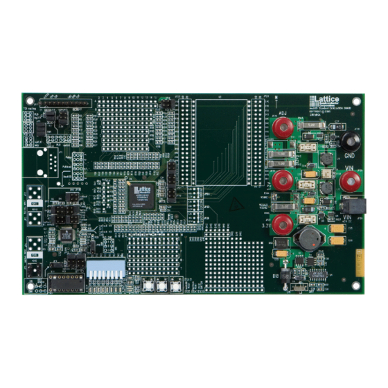
The MachXO Standard Evaluation board provides a convenient platform to evaluate electrical characteristics of the MachXO device, and to evaluate, test and de-bug custom logic designs. The board features a MachXO device in a 256-ball fpBGA package. The MachXO I/Os are connected to a rich variety of interfaces, including an 8-bit input switch, LEDs, PCB test points, 0.10”... -
Page 3: Additional Resources
Setting all of the 8-bit input switches to OFF reverses the direction of the count. If the switches are not all ON or all OFF, the LEDs for the switches that are ON will light up. Additionally, other I/Os on the MachXO device are also toggled using the internal counter outputs. -
Page 4: Power Supply
Power Supply The MachXO Standard Evaluation Board includes two locations to apply power. On the east side of the board are a pair of banana jacks (JP28 and JP29) and a coaxial DC connector (JP30), which receive power from either a bench power supply or a brick style power supply. - Page 5 Important Note: The board must be un-powered when connecting, disconnecting, or reconnecting the ispDOWN- LOAD Cable. Always connect the ispDOWNLOAD Cable's GND pin (black wire), before connecting any other JTAG pins. Failure to follow these procedures can in result in damage to the MachXO device and render the board inop- erable.
-
Page 6: Machxo And Support Interfaces
When pressed, LED D10 (yellow) illuminates. Adjacent, westward, to S2 is diode D11 (green). This is a LED tied to a general purpose I/O on the MachXO. This LED signals that the MachXO is done being programmed. However, it can be used to signal any status desired. - Page 7 Consult the MachXO device datasheet for further details regarding the MachXO pinout. Prototype Grid 1 and 2: Grid 1 is located in the northwest portion of the board. Grid 2 is due south of the MachXO device. Both areas have an alphanumeric grid located in the silkscreen indicating which plated through hole is attached to which MachXO pin.
- Page 8 5-6: 3.3V Prototype Grid 3: Just west (left) of the MachXO is a small array of nine test points. The MachXO I/O pin connec- tions are indicated in the silkscreen marking. For example, the top-left location connects to MachXO pin F5, etc.
- Page 9 U3 and JP23/JP24. JP23 and JP24 can then be populated with general-purpose headers. Jumpers can then be used to control connections between the MachXO device pins and the LCD. When this LCD is not populated (default condition), the outer columns of JP23 and JP24 can be used as general-...
- Page 10 Switches The evaluation board includes an eight-bit input toggle switch at the south edge of the board. The MachXO I/O location for each bit in the switch is indicated on the PCB silkscreen. When in the up position, the switch is pulled to 3.3V via a 10K resistor.
- Page 11 Pin 1 Note: XU2 pin 9 is routed to one of the two PLLs included on larger MachXO devices. These MachXO PLLs are not available on the MachXO640 device. XU2 pin 9 provides input to the PLL_T input pin M5.
- Page 12 The ispClock5610 has multiple configuration pins. The evaluation board includes a number of headers on the board allowing these configuration pins to be asserted, deasserted, or controlled from the MachXO. The headers have a general format as shown in Figure 7.
-
Page 13: Ordering Information
Mictor Header The left-side I/Os on the MachXO which are not used for the RJ-45 and small prototype test points are routed to a AMP/Tyco Mictor connector for additional off-board expansion. This connector can be mounted on the bottom side of the board. -
Page 14: Appendix A. Pcb Schematic
MachXO Standard Evaluation Board Lattice Semiconductor Revisions 001 & 002 User’s Guide Appendix A. PCB Schematic Figure 8. MachXO Control and Programming Interfaces... - Page 15 MachXO Standard Evaluation Board Lattice Semiconductor Revisions 001 & 002 User’s Guide Figure 9. MachXO I/O Connections...
- Page 16 MachXO Standard Evaluation Board Lattice Semiconductor Revisions 001 & 002 User’s Guide Figure 10. Power Section...
- Page 17 MachXO Standard Evaluation Board Lattice Semiconductor Revisions 001 & 002 User’s Guide Figure 11. Miscellaneous Interfaces...
- Page 18 MachXO Standard Evaluation Board Lattice Semiconductor Revisions 001 & 002 User’s Guide Figure 12. ispClock5610 Connections...
- Page 19 MachXO Standard Evaluation Board Lattice Semiconductor Revisions 001 & 002 User’s Guide Figure 13. LED and LCD Connections...
- Page 20 MachXO Standard Evaluation Board Lattice Semiconductor Revisions 001 & 002 User’s Guide Figure 14. Miscellaneous...
- Page 21 MachXO Standard Evaluation Board Lattice Semiconductor Revisions 001 & 002 User’s Guide Figure 15. Prototype Area...
- Page 22 MachXO Standard Evaluation Board Lattice Semiconductor Revisions 001 & 002 User’s Guide Figure 16. Prototype Area (Cont.)
- Page 23 MachXO Standard Evaluation Board Lattice Semiconductor Revisions 001 & 002 User’s Guide Figure 17. Prototype Area (Cont.)
- Page 24 MachXO Standard Evaluation Board Lattice Semiconductor Revisions 001 & 002 User’s Guide Figure 18. Prototype Area (Cont.)
- Page 25 Mouser Electronics Authorized Distributor Click to View Pricing, Inventory, Delivery & Lifecycle Information: Lattice LCMXO640C-L-EV LS-X2280-BASE-PC-N...
Need help?
Do you have a question about the MachXO and is the answer not in the manual?
Questions and answers