
Subscribe to Our Youtube Channel
Related Manuals for protech SP-7145


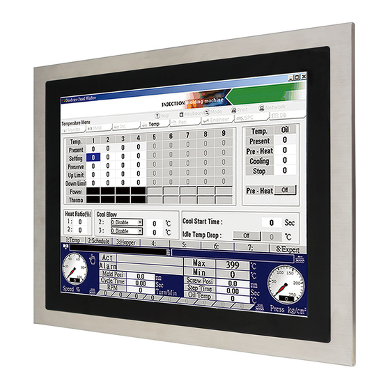
Summary of Contents for protech SP-7145
- Page 1 USER MANUAL SP-7145/7147 15” / 17” Fanless Panel PC Powered by Intel Atom E3845 / ® ® Celeron J1900 CPU Processor ® With DVI-I, 3COM, 4USB & 2LAN SP-7145/7147 M2...
- Page 2 SP-7145/7147 15”/17” High Performance Panel PC COPYRIGHT NOTICE & TRADEMARK All trademarks and registered trademarks mentioned herein are the property of their respective owners. This manual is copyrighted in August 2017. You may not reproduce or transmit in any form or by any means, electronic, or mechanical, including photocopying and recording.
- Page 3 FCC NOTICE This equipment has been tested and found to comply with the limits for a Class A digital device, pursuant to part 15 of the FCC Rules. These limits are designed to provide reasonable protection against harmful interference when the equipment is operated in a commercial environment.
-
Page 4: Table Of Contents
Rear I/O Ports Diagram (DC IN: 12V) ....... 3-2 JUMPER & CONNECTOR QUICK REFERENCE TABLE ..3-2 COMPONENT LOCATIONS ............. 3-3 3.3.1 Top View and Jumper Settings of SP-7145/7147 ....3-3 Setting Jumpers ................ 3-5 Setting Main Board Connectors and Jumpers ......3-7 3.5.1 LVDS POWER SELECTION .......... - Page 5 3.5.7 COM3 PIN9 DEFINITION SELECTION GUIDE ....3-13 3.5.8 COM4 VOLTAGE SELECTION ........3-14 3.5.9 AUDIO PORT ..............3-15 3.5.10 BATTERY WAFER ............3-16 3.5.11 COM2 and COM3 PORTS ..........3-16 3.5.12 COM4 CONNECTOR ............3-17 3.5.13 COM5 CONNECTOR ............3-18 3.5.14 COM6 CONNECTOR ............
- Page 6 3.8.1 RS-485 AUTO FLOW CONTROL FOR JCOM1_1 & JCOM1 ..................3-34 3.8.2 RS-232/422/485 SELECTION FOR JCOM1_1 & JCOM1 ..................3-35 3.8.3 RS-485 AUTO FLOW CONTROL FOR JCOM2_1 ..3-36 3.8.4 RS-232/422/485 SELECTION FOR JCOM2_1 ....3-37 DAUGHTER BOARD SR-6100 CONNECTOR & JUMPER QUICK REFERENCE TABLE ..........
- Page 7 Installing Sound Driver Utility ..........4-10 Installing Resistive Touch Driver Utility ........4-10 Installing Projected Capacitive Touch Driver Utility ....4-11 BIOS SETUP ..................5-1 Introduction ................5-2 Accessing Setup Utility .............. 5-3 Main ................... 5-7 Advanced .................. 5-9 5.4.1 Advanced –...
- Page 8 Appendix A System Diagrams ............1 SP-7145 System Exploded Diagram ..............2 SP-7145 Touch Panel & LCD Display Exploded Diagram ......3 SP-7145 Touch Panel & LCD Display Exploded Diagram ......5 SP-7145 Touch Panel & LCD Display Exploded Diagram ......7 SP-7145 Touch Panel &...
- Page 9 List of Figures Figure 3-1. Main Board Component Location (Top View) ....3-3 Figure 3-2. Daughter Board BR-6062 Component Location (Top View) .................. 3-33 Figure 3-2. Daughter Board SR-6100 Component Location (Top View) .................. 3-38 Figure 5-1. Extensible Firmware Interface Diagram ......5-2 Figure 5-2.
-
Page 10: Revision History
Revision History The revision history of SP-7145/7147 User Manual is described below: Version No. Revision History Date Initial Release 2017/06/27 1. SP-7145/7147 system diagrams have been changed. 2. SP-7145/7147 rear I/O ports diagrams 2017/08/15 have been changed. 3. SP-7145/7147 exploded diagrams have... -
Page 11: Introduction
Introduction This chapter provides the introduction for the SP-7145/7147 system as well as the framework of the user manual. The following topic is included: • About This Manual SP-7145/7147 SERIES USER MANUAL Page: 1-1... -
Page 12: About This Manual
Chapter 1 Introduction About This Manual Thank you for purchasing our SP-7145/7147 system. The SP-7145/7147 is an updated system designed to be comparable with the highest performance of IBM AT personal computers. The SP-7145/7147 provides faster processing speed, greater expandability and can handle more tasks than before. -
Page 13: Getting Started
Getting Started This chapter provides the information for the SP-7145/7147 system. It describes how to set up the system quickly and outlines the system specifications. The following topics are included: • Package List • System Overview • System Diagrams • System Specification •... -
Page 14: Package List
If you discover any of the items listed below are damaged or lost, please contact your local distributor immediately. Item Q’ty SP-7145/7147 Manual / Driver DVD Quick Guide AC Power Cord Power Adapter Power Adapter Cable SP-7145/7147 SERIES USER MANUAL Page: 2-2... -
Page 15: System Diagrams
Chapter 2 Getting Started System Diagrams Unit: mm SP-7145 Front View Rear View Top View SP-7145/7147 SERIES USER MANUAL Page: 2-3... - Page 16 Chapter 2 Getting Started Bottom View DC-IN: 9 ~ 36V DC-IN: 12V Unit: mm Left Side View Right Side View SP-7145/7147 SERIES USER MANUAL Page: 2-4...
- Page 17 Chapter 2 Getting Started Quarter View SP-7145/7147 SERIES USER MANUAL Page: 2-5...
- Page 18 Chapter 2 Getting Started SP-7147 Unit: mm Front View Rear View Top View SP-7145/7147 SERIES USER MANUAL Page: 2-6...
- Page 19 Chapter 2 Getting Started Bottom View DC-IN: 9 ~ 36V DC-IN: 12V Unit: mm Left Side View Right Side View SP-7145/7147 SERIES USER MANUAL Page: 2-7...
- Page 20 Chapter 2 Getting Started Quarter View SP-7145/7147 SERIES USER MANUAL Page: 2-8...
-
Page 21: System Specifications
1 x half-sized Mini PCIe slot Mounting Support Wall mount / VESA 75 / VESA 100 / Panel mount SP-7145: 6.8 kg, 408mm x 320mm x 26mm Net Weight & SP-7147: 7.9 kg, 436mm x 368mm x 27.4mm Dimension (WxHxD) Certificate ... - Page 22 0°C ~55°C SSD (with J1900) -20°C ~50°C SSD (with E3845, Sunlight readable panel) -20°C ~55°C SSD (with E3845) Storage Temp. -20°C ~ 80°C (-4°F ~ 176°F) Humidity 20%~ 90% SP-7145/7147 SERIES USER MANUAL Page: 2-10...
-
Page 23: Safety Precautions
Avoid direct sunlight exposure for a long period of time (for example, in a closed car in summer time. Also avoid the system from any heating device.). Or do not use SP-7145/7147 when it has been left outdoors in a cold winter day. -
Page 24: System Configuration
• External I/O Ports Diagram • Main Board Jumper Settings and Component Locations • How to Set Jumpers • Setting Main Board Connectors and Jumpers • Daughter Board Component Locations • Setting Daughter Board Connectors and Jumpers SP-7145/7147 SERIES USER MANUAL Page: 3-1... -
Page 25: External I/O Ports Diagrams
(optional) Connector Remote LAN2 (optional) Switch LAN1 COM4 COM5 DC IN 12V Remote SW LAN1 LAN2 PS/2 Power COM6 COM2 COM1 Button COM3 DVI-I USB2.0/2.0 USB2.0/3.0 DVI-I Line-out PS/2 Mouse/ Mic-in Connector Keyboard Connector SP-7145/7147 SERIES USER MANUAL Page: 3-2... -
Page 26: Jumper & Connector Quick Reference Table
JLAN_USB1 LAN& USB2.0/3.0 Port JLAN_USB2 LVDS Connector JLVDS1 SATA Connector JSATA1, JSATA2 SATA Power Connector JSATA_PWR1, JSATA_PWR2 USB Connector JUSB1 MINI PCIE Connector M_PCI_E1 PCIE BUS PCI_E1 LPC Connector JLPC1 Clear CMOS Data Selection SP-7145/7147 SERIES USER MANUAL Page: 3-2... -
Page 27: Component Locations
Chapter 3 Hardware Configuration COMPONENT LOCATIONS 3.3.1 Top View and Jumper Settings of SP-7145/7147 Figure 3-1 Main Board Component Location (Top View) WARNING: Always disconnect the power cord when you are working with connectors and jumpers on the main board. - Page 28 CAUTION: Always touch the motherboard components by the edges. Never touch components such as a processor by its pins. Take special cares while you are holding electronic circuit boards by the edges only. Do not touch the mainboard components. SP-7145/7147 SERIES USER MANUAL Page: 3-4...
-
Page 29: Setting Jumpers
2 to create one setting and shorting. You can also select to connect pins 2 and 3 to create another setting. The format of the jumper picture will be illustrated throughout this manual. The figure below shows different types of jumpers and jumper settings. SP-7145/7147 SERIES USER MANUAL Page: 3-5... - Page 30 Chapter 3 Hardware Configuration Jumper diagrams Jumper settings SP-7145/7147 SERIES USER MANUAL Page: 3-6...
-
Page 31: Setting Main Board Connectors And Jumpers
Chapter 3 Hardware Configuration Setting Main Board Connectors and Jumpers 3.5.1 LVDS POWER SELECTION JP4: LVDS Power Selection SELECTION JUMPTER SETTING JUMPER ILLUSTRATION 3.3V Note: Manufacturing default for SP-7145 is 3.3V. Manufacturing default for SP-7147 is 5V. SP-7145/7147 SERIES USER MANUAL Page: 3-7... -
Page 32: Backlight Inverter Pwm Voltage Selection
Chapter 3 Hardware Configuration 3.5.2 BACKLIGHT INVERTER PWM VOLTAGE SELECTION JP5: Backlight Inverter PWM Voltage Selection SELECTION JUMPTER SETTING JUMPER ILLUSTRATION 3.3V Note: Manufacturing default for SP-7145 is 3.3V. Manufacturing default for SP-7147 is 5V. SP-7145/7147 SERIES USER MANUAL Page: 3-8... -
Page 33: Power-On Mode Selection
Select by BIOS Note 1: Manufacturing default is Auto-on. Note 2: Manufacturing default for BS-H292 (SBOX) is "NC". Note 3: Auto-On means that system will turn on automatically whenever the main power is restored. SP-7145/7147 SERIES USER MANUAL Page: 3-9... -
Page 34: Backlight Enable Selection
Chapter 3 Hardware Configuration 3.5.4 BACKLIGHT ENABLE SELECTION JP9: BACKLIGHT ENABLE Selection SELECTION JUMPTER SETTING JUMPER ILLUSTRATION 3.3V Note: Manufacturing default for SP-7145 is 3.3V. Manufacturing default for SP-7147 is 5V. SP-7145/7147 SERIES USER MANUAL Page: 3-10... -
Page 35: Vga/Dvi Selection
Chapter 3 Hardware Configuration 3.5.5 VGA/DVI SELECTION JP10: VGA/DVI Selection SELECTION JUMPTER SETTING JUMPER ILLUSTRATION (1-3) (5-6) JP10 (1-2) (4-6) JP10 Note: Manufacturing default is DVI. SP-7145/7147 SERIES USER MANUAL Page: 3-11... -
Page 36: Lvds Resolution Selection
LVDS RESOLUTION SELECTION JP14 & JP15: LVDS Resolution Selection SELECTION JUMPTER SETTING JUMPER ILLUSTRATION JP15(4-6) 1024x768 JP15(3-5) 1CH/24bit JP14(2-4) (for SP-7145) JP14 JP15 JP14(3-5) JP15(4-6) 1280x1024 JP15(1-3) 2CH/24bit JP14(2-4) (for SP-7147) JP14 JP15 JP14(3-5) SP-7145/7147 SERIES USER MANUAL Page: 3-12... -
Page 37: Com3 Pin9 Definition Selection Guide
Chapter 3 Hardware Configuration 3.5.7 COM3 PIN9 DEFINITION SELECTION GUIDE JP_COM3: COM3 Port pin9 RI/5V/12V Selection SELECTION JUMPTER SETTING JUMPER ILLUSTRATION JP_COM3 JP_COM3 JP_COM3 Note: Manufacturing default is RI. SP-7145/7147 SERIES USER MANUAL Page: 3-13... -
Page 38: Com4 Voltage Selection
Chapter 3 Hardware Configuration 3.5.8 COM4 VOLTAGE SELECTION JP_COM4: COM4 Voltage Selection SELECTION JUMPTER SETTING JUMPER ILLUSTRATION JP_COM4 JP_COM4 JP_COM4 Note 1: Manufacturing default is RI. Note 2: Manufacturing default for BS-H292 (SBOX)) is 5V (5-6). SP-7145/7147 SERIES USER MANUAL Page: 3-14... -
Page 39: Audio Port
Chapter 3 Hardware Configuration 3.5.9 AUDIO PORT JAUDIO1: Line-In, Line-Out & Microphone The connector can also support only Microphone. Line-In: ASSIGNMENT LINE-IN-L LINE-IN-R Line-Out: ASSIGNMENT LINE-OUT-L LINE-OUT-R Mic-In: JAUDIO1 ASSIGNMENT MIC_L MIC_R Others: ASSIGNMENT SP-7145/7147 SERIES USER MANUAL Page: 3-15... -
Page 40: Battery Wafer
Chapter 3 Hardware Configuration 3.5.10 BATTERY WAFER JBAT1: Battery Wafer ASSIGNMENT RTC_BAT JBAT1 3.5.11 COM2 and COM3 PORTS JCOM2_3: COM Port ASSIGNMENT JCOM2_3 SP-7145/7147 SERIES USER MANUAL Page: 3-16... -
Page 41: Com4 Connector
Chapter 3 Hardware Configuration 3.5.12 COM4 CONNECTOR JCOM4: COM4 Connector ASSIGNMENT ASSIGNMENT JCOM4 SP-7145/7147 SERIES USER MANUAL Page: 3-17... -
Page 42: Com5 Connector
Chapter 3 Hardware Configuration 3.5.13 COM5 CONNECTOR JCOM5: COM5 Connector ASSIGNMENT ASSIGNMENT JCOM5 3.5.14 COM6 CONNECTOR JCOM6: COM6 Connector ASSIGNMENT ASSIGNMENT JCOM6 SP-7145/7147 SERIES USER MANUAL Page: 3-18... -
Page 43: Dvi-I & Com Port
3.5.15 DVI-I & COM PORT JCOM_DVII1: DVI-I & COM PORT DVI-I: DVI Connector ASSIGNMENT ASSIGNMENT TMDS_D2- TMDS_D2+ DDC_CLK DDC_DATA VSYNC TMDS_D1- TMDS_D1+ TMDS_D0- TMDS_D0+ JCOM_DVII1 TMDS_CLK+ TMDS_CLK- GREEN BLUE HSYNC COM1: COM Connector ASSIGNMENT SP-7145/7147 SERIES USER MANUAL Page: 3-19... -
Page 44: Fan Connector
Chapter 3 Hardware Configuration 3.5.16 FAN CONNECTOR JCPU_FAN1, JSYS_FAN1: Fan Connector ASSIGNMENT FAN_CONTROL FAN_SIGNAL JCPU_FAN1/ JSYS_FAN1 3.5.17 DC 12V CONNECTOR JDC_PWR1: DC 12V Connector ASSIGNMENT JDC_PWR1 SP-7145/7147 SERIES USER MANUAL Page: 3-20... -
Page 45: Dio Wafer (Optional)
ASSIGNMENT DIN0 DOUT0 JDIO1 DIN1 DOUT1 DIN2 DOUT2 DIN3 DOUT3 3.5.19 FRONT CONNECTOR JFP1: Front Connector ASSIGNMENT ASSIGNMENT HDD_LED+ RESET SWITCH PWR_LED+ SPEAKER SIGNAL HDD_LED- POWER BUTTON PWR_LED- SPEAKER SIGNAL SPK_VCC SPEAKER SIGNAL JFP1 SP-7145/7147 SERIES USER MANUAL Page: 3-21... -
Page 46: Inverter Wafer
Chapter 3 Hardware Configuration 3.5.20 INVERTER WAFER JINV1: Inverter Wafer ASSIGNMENT PWM SIGNAL JINV1 BACKLIGHT EN SP-7145/7147 SERIES USER MANUAL Page: 3-22... -
Page 47: Kb/Ms Port
Chapter 3 Hardware Configuration 3.5.21 KB/MS PORT JKB_MS1: KB/MS Port Keyboard: ASSIGNMENT DATA Mouse: ASSIGNMENT DATA JKB_MS1 SP-7145/7147 SERIES USER MANUAL Page: 3-23... -
Page 48: Lan & Usb2.0 Port
Chapter 3 Hardware Configuration 3.5.22 LAN & USB2.0 PORT Yellow Orange/ JLAN_USB1: LAN & USB2.0 PORT Green USB2.0: LAN: ASSIGNMENT ASSIGNMENT TX_D1+ TX_D1- RX_D2+ BI_D3+ BI_D3- RX_D2- BI_D4+ BI_D4- JLAN_USB1 SP-7145/7147 SERIES USER MANUAL Page: 3-24... -
Page 49: Lan& Usb2.0/3.0 Port
Chapter 3 Hardware Configuration 3.5.23 LAN& USB2.0/3.0 PORT JLAN_USB2: LAN & USB2.0/3.0 PORT Yellow Orange/ LAN: ASSIGNMENT Green TX_D1+ TX_D1- RX_D2+ BI_D3+ BI_D3- RX_D2- BI_D4+ BI_D4- USB2.0: ASSIGNMENT VBUS STDA_SSRX- STDA_SSRX+ JLAN_USB2 STDA_SSTX- STDA_SSTX+ SP-7145/7147 SERIES USER MANUAL Page: 3-25... -
Page 50: Lvds Connector
Chapter 3 Hardware Configuration 2-28. LVDS CONNECTOR JLVDS1: LVDS Connector JLVDS1 ASSIGNMENT ASSIGNMENT LVDS_VCC LVDS1_CLK- LVDS1_CLK+ LVDS1_D2- LVDS1_D2+ LVDS1_D1- LVDS1_D1+ LVDS1_D3+ LVDS1_D3- LVDS1_D0+ LVDS1_D0- LVDS0_CLK+ LVDS0_CLK- LVDS0_D2+ LVDS0_D2- LVDS0_D1+ LVDS0_D1- LVDS0_D0+ LVDS0_D0- LVDS0_D3+ LVDS0_D3- LVDS_VCC LVDS_VCC SP-7145/7147 SERIES USER MANUAL Page: 3-26... -
Page 51: Sata Connector
Chapter 3 Hardware Configuration 3.5.24 SATA CONNECTOR JSATA1, JSATA2: Two Serial ATA Connectors ASSIGNMENT JSATA1/ JSATA2 2-30. SATA POWER CONNECTOR JSATA_PWR1, JSATA_PWR2: SATA Power Connector ASSIGNMENT JSATA_PWR1/ JSATA_PWR2 SP-7145/7147 SERIES USER MANUAL Page: 3-27... -
Page 52: Usb Connector
Chapter 3 Hardware Configuration 3.5.25 USB CONNECTOR JUSB1: USB Connector ASSIGNMENT ASSIGNMENT JUSB1 SP-7145/7147 SERIES USER MANUAL Page: 3-28... -
Page 53: Mini Pcie Connector
Chapter 3 Hardware Configuration 3.5.26 MINI PCIE CONNECTOR M_PCI_E1: MINI PCIE Connector ASSIGNMENT ASSIGNMENT WAKE# 3.3V M_PCI_E1 1.5V CLKREQ# REFCLK- REFCLK+ PERST# PERn0 3.3V PERp0 1.5V SMB_CLK PETn0 SMB_DATA PETp0 USB_D- USB_D+ 3.3V 3.3V 1.5V 3.3V SP-7145/7147 SERIES USER MANUAL Page: 3-29... -
Page 54: Pcie Bus
Chapter 3 Hardware Configuration 3.5.27 PCIE BUS PCI_E1: PCIE BUS ASSIGNMENT ASSIGNMENT SMB_CLK SMB_DATA 3.3V 3.3V 3.3V 3.3V_SB PWRGD WAKE# PCI_E1 REFCLK+ REFCLK- HSOP0 HSON0 HSIP0 HSIN0 PRSNT# SP-7145/7147 SERIES USER MANUAL Page: 3-30... -
Page 55: Lpc Connector
Chapter 3 Hardware Configuration 3.5.28 LPC CONNECTOR JLPC1: LPC Connector ASSIGNMENT ASSIGNMENT FRAME RESET VCC5 LAD3 LAD2 VCC3 LAD1 JLPC1 LAD0 SMBCLK SMBDATA 3VSB SERIRQ CLK RUN SUS_TAT DREQ0 SP-7145/7147 SERIES USER MANUAL Page: 3-31... -
Page 56: Clear Cmos Data Selection
Step 4. Power on the PC and the PC will then auto-reboot for once in order to set SoC’s register. Step 5. Done! SELECTION JUMPER SETTINGS JUMPER ILLUSTRATION Open Normal (Default Setting) Clear CMOS Close Data Note: Please make sure the main power is off before you clear CMOS. SP-7145/7147 SERIES USER MANUAL Page: 3-32... -
Page 57: Daughter Board Br-6062 Jumper Quick Reference
RS-232/422/485 Selection for JCOM1_1 & JCOM1 RS-485 Auto Flow Control for JCOM2_1 RS-232/422/485 Selection for JCOM2_1 COMPONENT LOCATIONS DAUGHTER BOARD BR-6062 3.7.1 BR-6062 Top View Figure 3-2 Daughter Board BR-6062 Component Location (Top View) SP-7145/7147 SERIES USER MANUAL Page: 3-33... -
Page 58: Setting Daughter Board Br-6062 Jumpers
Chapter 3 Hardware Configuration SETTING DAUGHTER BOARD BR-6062 JUMPERS 3.8.1 RS-485 AUTO FLOW CONTROL FOR JCOM1_1 & JCOM1 JP1: RS-485 Auto Flow Control Selection for JCOM1_1 and JCOM1 JUMPTER SELECTION JUMPER ILLUSTRATION SETTING Normal (Default) Auto SP-7145/7147 SERIES USER MANUAL Page: 3-34... -
Page 59: Rs-232/422/485 Selection For Jcom1_1 & Jcom1
Chapter 3 Hardware Configuration 3.8.2 RS-232/422/485 SELECTION FOR JCOM1_1 & JCOM1 JP2: RS-232/422/485 Selection for JCOM1_1 & JCOM1 Selection Jumper Setting Jumper Illustration RS-232 Open (Default) RS-422 1-2, 3-4, 9-10 RS-485 1-2, 5-6, 7-8 SP-7145/7147 SERIES USER MANUAL Page: 3-35... -
Page 60: 3.8.3 Rs-485 Auto Flow Control For Jcom2_1
Chapter 3 Hardware Configuration 3.8.3 RS-485 AUTO FLOW CONTROL FOR JCOM2_1 JP3: RS-485 Auto Flow Control Selection for JCOM2_1 JUMPTER SELECTION JUMPER ILLUSTRATION SETTING Normal (Default) Auto SP-7145/7147 SERIES USER MANUAL Page: 3-36... -
Page 61: Rs-232/422/485 Selection For Jcom2_1
Chapter 3 Hardware Configuration 3.8.4 RS-232/422/485 SELECTION FOR JCOM2_1 JP4: RS-232/422/485 Selection for JCOM2_1 Selection Jumper Setting Jumper Illustration RS-232 Open (Default) RS-422 1-2, 3-4, 9-10 RS-485 1-2, 5-6, 7-8 SP-7145/7147 SERIES USER MANUAL Page: 3-37... -
Page 62: Daughter Board Sr-6100 Connector & Jumper
Continuous Mode Selection CONNECTOR NAME VIN Voltage Selection (+9V ~ +36V) VOUT VOUT Voltage Selection (+12V) 3.10 COMPONENT LOCATIONS DAUGHTER BOARD SR-6100 3.10.1 SR-6100 Top View Figure 3-3 Daughter Board SR-6100 Component Location (Top View) SP-7145/7147 SERIES USER MANUAL Page: 3-38... -
Page 63: Setting Daughter Board Sr-6100 Connectors
Chapter 3 Hardware Configuration 3.11 SETTING DAUGHTER BOARD SR-6100 CONNECTORS & JUMPERS 3.11.1 VIN Connector (+9V~+36V) VIN: VIN Connector ASSIGNMENT VIN+ VIN+ 3.11.2 VOUT Connector (+12V) VIN: VIN Connector ASSIGNMENT VOUT VOUT VOUT SP-7145/7147 SERIES USER MANUAL Page: 3-39... -
Page 64: Run Control Input Selection
Chapter 3 Hardware Configuration 3.11.3 RUN CONTROL INPUT SELECTION JP1: Run Control Input Selection JUMPTER SELECTION JUMPER ILLUSTRATION SETTING VIN+ (Turn On) (Default) (Shut Down) SP-7145/7147 SERIES USER MANUAL Page: 3-40... -
Page 65: Pulse Skipping Mode Selection
PULSE SKIPPING MODE SELECTION JP2/JP3: Pulse Skipping Mode Selection JUMPTER SELECTION JUMPER ILLUSTRATION SETTING Pulse Skipping Mode (Default) Open 3.11.5 CONTINUOUS MODE SELECTION JP2/JP3: Continuous Mode Selection JUMPTER SELECTION JUMPER ILLUSTRATION SETTING Open Continuous Mode (Default) SP-7145/7147 SERIES USER MANUAL Page: 3-41... -
Page 66: Software Utilities
• Installing Graphics Driver Utility • Installing LAN Driver Utility • Installing Intel ® USB 3.0 eXtensible Host Controller Utility • Installing Sound Driver Utility • Installing Resistive Touch Driver Utility • Installing Projected Capacitive Touch Driver Utility SP-7145/7147 SERIES USER MANUAL Page: 4-1... -
Page 67: Introduction
Chapter 4 Software Utilities Introduction Enclosed with the SP-7145/7147 Series package is our driver utilities contained in a DVD-ROM disk. Refer to the following tables for driver locations: Filename (Assume that Purpose DVD- ROM drive is D:) Win7/32 bit For Aptio(EFI) BIOS update ... - Page 68 D:\Driver\Platform\Sound Realtek ALC888S For Codec Sound driver installation Resistive touch driver D:\Driver\Device\touch driver installation X : Not support : Support Note: Install the driver utilities immediately after the OS installation is completed. SP-7145/7147 SERIES USER MANUAL Page: 4-3...
- Page 69 D:\Driver\Platform\Sound Realtek ALC888S For Codec Sound driver installation Resistive touch driver D:\Driver\Device\touch driver installation X : Not support : Support Note: Install the driver utilities immediately after the OS installation is completed. Page: 4-4 SP-7145/7147 SERIES USER MANUAL...
-
Page 70: Intel ® Chipset Software Installation Utility
7/10 series, and it should be installed immediately after the OS installation is finished. Please follow the steps below: Connect the USB DVD-ROM device to SP-7145/7147 and insert the driver disk. Enter the Main Chip folder where the Chipset driver is located. -
Page 71: Intel ® Trusted Execution Engine Installation Utility
Installation Instructions for Intel Trusted Execution Engine Installation Utility Connect the USB DVD-ROM device to SP-7145/7147 and insert the driver disk. Enter the TXE folder where the driver is located. Select Windows 7 (32/64-bit) / Windows 10 (32/64-bit) for your OS platform. -
Page 72: Installing Graphics Driver Utility
SP-7145/7147 for the changes to take effect. Installing Graphics Driver Utility The graphics interface embedded in SP-7145/7147 can support a wide range of display types. You can have dual displays via DVI-D ports and make the system work simultaneously. -
Page 73: Installing Lan Driver Utility
Installing LAN Driver Utility Enhanced with LAN function, SP-7145/7147 supports various network adapters. To install the LAN Driver, follow the steps below: Connect the USB DVD-ROM device to SP-7145/7147 and insert the driver disk. Enter the LAN folder where the driver is located. -
Page 74: Intel® Usb 3.0 Extensible Host Controller Utility
To install the utility, follow the steps below: Insert the driver disk into a DVD-ROM device. Under Windows system, go to the directory where the driver is located. Run the application with administrative privileges. SP-7145/7147 SERIES USER MANUAL Page: 4-9... -
Page 75: Installing Sound Driver Utility
Windows 7/10 series. To install the Sound Driver, follow the steps below: Connect the USB DVD-ROM device to SP-7145/7147 and insert the driver disk. Open the Sound folder where the driver is located. Select Windows 7 (32/64-bit) / Windows 10 (32/64-bit) for your OS platform. -
Page 76: Installing Projected Capacitive Touch Driver Utility
Installing Projected Capacitive Touch Driver Utility To install the Projected Capacitive Touch Driver, follow the steps below: Connect the USB DVD-ROM device to SP-7145/7147 and insert the driver disk. Enter the Touch driver > WES7 folder where the driver is located. -
Page 77: Bios Setup
The BIOS Setup Utilities consist of the following menu items: Accessing Setup Utilities • Main Menu • Advanced Menu • Chipset Menu • Security Menu • Boot Menu • Save & Exit Menu • SP-7145/7147 SERIES USER MANUAL Page: 5-1... -
Page 78: Introduction
Chapter 5 BIOS Setup Introduction The SP-7145/7147 System uses an AMI (American Megatrends Aptio BIOS that is stored in the Serial Peripheral Interface Incorporated) Flash Memory (SPI Flash) and can be updated. The SPI Flash contains the built-in BIOS setup program, Power-On Self-Test (POST), PCI auto-configuration utility, LAN EEPROM information, and Plug and Play support. -
Page 79: Accessing Setup Utility
All the menu settings are described in details in this chapter. Accessing Setup Utility After the system is powered on, BIOS will enter the Power-On Self-Test (POST) routines and the POST message will be displayed: SP-7145/7147 SERIES USER MANUAL Page: 5-3... -
Page 80: Figure 5-2. Post Screen With Ami Logo
Chapter 5 BIOS Setup Figure 5-2. POST Screen with AMI Logo Press <Del> or <Esc> to access the Setup Utility program and the Main menu of the Aptio Setup Utility will appear on the screen as below: SP-7145/7147 SERIES USER MANUAL Page: 5-4... - Page 81 US English. You may use <↑> or <↓> key to select among the items and press <Enter> to confirm and enter the sub-menu. The following table provides the list of the navigation keys that you can use while operating the BIOS setup menu. SP-7145/7147 SERIES USER MANUAL Page: 5-5...
- Page 82 The CMOS battery The battery may be losing power and users is bad or has been should replace the battery immediately. Also, this message is displayed once the new battery recently replaced. is replaced. SP-7145/7147 SERIES USER MANUAL Page: 5-6...
-
Page 83: Main
Build Date and No changeable options Displays the date of current BIOS version. Time BayTrail SoC No changeable options SoC stepping (BayTrail-I only) Sec RC Version No changeable options Displays the current Sec RC version. SP-7145/7147 SERIES USER MANUAL Page: 5-7... - Page 84 The “Day” is automatically changed. System Time Hour, minute, second Sets the system time. The format is [Hour: Minute: Second]. Users can directly enter values or use <+> or <-> arrow keys to increase/decrease it. SP-7145/7147 SERIES USER MANUAL Page: 5-8...
-
Page 85: Advanced
Super I/O Chip Configuration. Configuration Hardware Monitor Sub-Menu Monitor hardware status F81866 Watchdog Sub-Menu F81866 Watchdog Parameters. CPU Configuration Sub-Menu CPU Configuration. Parameters. IDE Configuration Sub-Menu SATA Configuration Parameters. OS Selection Sub-Menu OS Selection (BayTrail-D only). SP-7145/7147 SERIES USER MANUAL Page: 5-9... -
Page 86: Advanced - Trusted Computing (Baytrail-I Only)
O.S. will not show Security Device. TCG EFI Protocol and INT1A interface will not be available. TPM 1.2 will restrict support to TPM Device Select - TPM 1.2 1.2 devices.TPM 2.0 will restrict - TPM 2.0 SP-7145/7147 SERIES USER MANUAL Page: 5-10... -
Page 87: Advanced - Acpi Settings
Enable ACPI Auto - Disabled Enables or Disables ACPI feature. Configuration - Enabled Enable Hibernation - Disabled Enables or Disables System ability to - Enabled Hibernate (OS/S4 Sleep State). This option may be not effective with SP-7145/7147 SERIES USER MANUAL Page: 5-11... -
Page 88: Advanced - F81866 Super Io Configuration
Displays the super IO chip model and its options manufacturer. Sets the parameters of Serial Port 1 Serial Port 1 Configuration Sub-menu (COMA). Serial Port 2 Configuration Sub-menu Sets the parameters of Serial Port 2 SP-7145/7147 SERIES USER MANUAL Page: 5-12... - Page 89 Serial Port 1 Configuration Screen BIOS Setting Options Description/Purpose - Disabled Enables or Disables Serial Serial Port - Enabled Port 1. Displays the current settings Device Settings No changeable options of Serial Port 1. SP-7145/7147 SERIES USER MANUAL Page: 5-13...
- Page 90 No changeable options of Serial Port 2. Change Settings - IO=2F8h; IRQ=3 Allows you to select specific - IO=3F8h; IRQ=3,4,5,6,7,9,10,11,12 IO address and IRQ for Serial - IO=2F8h; IRQ=3,4,5,6,7,9,10,11,12 Port 2. - IO=3E8h;IRQ=3,4,5,6,7,9,10,11,12 - IO=2E8h;IRQ=3,4,5,6,7,9,10,11,12 SP-7145/7147 SERIES USER MANUAL Page: 5-14...
- Page 91 No changeable options of Serial Port 3. Change Settings - IO=3E8h; IRQ=10 Allows you to select specific - IO=3F8h; IRQ=3,4,5,6,7,9,10,11,12 IO address and IRQ for Serial - IO=2F8h; IRQ=3,4,5,6,7,9,10,11,12 Port 3. - IO=2F0h;IRQ=3,4,5,6,7,9,10,11,12 - IO=2E0h;IRQ=3,4,5,6,7,9,10,11,12 SP-7145/7147 SERIES USER MANUAL Page: 5-15...
- Page 92 Device Settings No changeable options of Serial Port 4. Change Settings - IO=2E8h; IRQ=5 Allows you to select specific - IO=3E8h;IRQ=3,4,5,6,7,9,10,11,12 IO address and IRQ for Serial - IO=2E8h;IRQ=3,4,5,6,7,9,10,11,12 Port 4. - IO=2F0h;IRQ=3,4,5,6,7,9,10,11,12 - IO=2E0h;IRQ=3,4,5,6,7,9,10,11,12 SP-7145/7147 SERIES USER MANUAL Page: 5-16...
- Page 93 Device Settings No changeable options of Serial Port 5. Change Settings - IO=2F0h; IRQ=7 Allows you to select specific - IO=3E8h;IRQ=3,4,5,6,7,9,10,11,12 IO address and IRQ for Serial - IO=2E8h;IRQ=3,4,5,6,7,9,10,11,12 Port 5. - IO=2F0h;IRQ=3,4,5,6,7,9,10,11,12 - IO=2E0h;IRQ=3,4,5,6,7,9,10,11,12 SP-7145/7147 SERIES USER MANUAL Page: 5-17...
- Page 94 Device Settings No changeable options of Serial Port 6. Change Settings - IO=2E0h; IRQ=7 Allows you to select specific - IO=3E8h;IRQ=3,4,5,6,7,9,10,11,12 IO address and IRQ for Serial - IO=2E8h;IRQ=3,4,5,6,7,9,10,11,12 Port 6. - IO=2F0h;IRQ=3,4,5,6,7,9,10,11,12 - IO=2E0h;IRQ=3,4,5,6,7,9,10,11,12 SP-7145/7147 SERIES USER MANUAL Page: 5-18...
-
Page 95: Advanced - Hardware Monitor
Boundary Temperature -5~10 Adjusts boundary Temperature Step. Step Segment Speed Count -20~60 Adjusts Segment Speed Count.(%)If set Segment Speed Count=60%, Step=10%, the segment speed will set 60% , 70%, 80% , 90% , 100% SP-7145/7147 SERIES USER MANUAL Page: 5-19... - Page 96 No changeable options the VSB5V in supply. VCC5 Detects and displays voltage level of No changeable options the VCC5V in supply. VCC12 Detects and displays voltage level of No changeable options the VCC12 in supply. SP-7145/7147 SERIES USER MANUAL Page: 5-20...
-
Page 97: Advanced - F81866 Watchdog Configuration
Selects 1s (second) or 60s (minute) as Watchdog timer unit - 60s the time unit of Watchdog timer. Count for Timer Numeric Sets the timeout for Watchdog timer. (Seconds) (from 1 to 255) (Max. value: 255 seconds or minutes) SP-7145/7147 SERIES USER MANUAL Page: 5-21... -
Page 98: Advanced - Cpu Configuration
No changeable options Reports if the processor supports Intel x86-64 (amd64) implementation. Intel Virtualization - Disabled When enabled, a VMM can utilize the Technology additional hardware capabilities - Enabled provided by Vanderpool Technology (VT).(BayTrail -D only) SP-7145/7147 SERIES USER MANUAL Page: 5-22... - Page 99 Reports if Intel Hyper-Threading Technology is supported by the processor Intel VT-x Technology No changeable options Reports if Intel VT-x Technology is supported by the processor. L1 Data Cache No changeable options Displays L1 Data Cache size. SP-7145/7147 SERIES USER MANUAL Page: 5-23...
- Page 100 Options Description/Purpose L1 Code Cache No changeable options Displays L1 Code Cache size. L2 Cache No changeable options Displays L2 Cache size. L3 Cache No changeable options Displays L3 Cache size. BayTrail-I SoC E3845 SP-7145/7147 SERIES USER MANUAL Page: 5-24...
-
Page 101: Advanced - Ide Configuration
Gen1 mode sets device to 1.5 Gbit/s - Gen2 speed. • Gen2 mode sets the device to 3 Gbit/s speed (in case it is compatible). SATA Mode - IDE mode Configures SATA as following: SP-7145/7147 SERIES USER MANUAL Page: 5-25... -
Page 102: Os Selection (Baytrail-D Only)
SATA Port 1 [drive] Displays the drive installed on this SATA port 1. Shows [Empty] if no drive is installed. (BayTrail-D only) 5.4.8 OS Selection (BayTrail-D only) Menu Path Advanced > OS Selection OS Selection Screen SP-7145/7147 SERIES USER MANUAL Page: 5-26... -
Page 103: Advanced - Csm Configuration
CSM Configuration Screen BIOS Setting Options Description/Purpose CSM Support - Disabled Enables or Disables CSM Support. - Enabled CSM16 Module No changeable options Displays the CSM 16 Module version. Version SP-7145/7147 SERIES USER MANUAL Page: 5-27... - Page 104 Controls the execution of UEFI and Legacy Video. - UEFI only - Legacy only Other PCI - UEFI first Select launch method for other PCI devices devices, such as NIC, mass storage or - Legacy only video card. SP-7145/7147 SERIES USER MANUAL Page: 5-28...
-
Page 105: Advanced - Usb Configuration
- Enabled only) EHCI Hand-off - Disabled This is a workaround for OSes without EHCI hand-off support. - Enabled USB Mass Storage Driver - Disabled Enables/Disables USB mass storage driver Support. support. - Enabled SP-7145/7147 SERIES USER MANUAL Page: 5-29... - Page 106 100 ms, for a Hub port the delay is taken from Hub descriptor. Mass Storage Devices: - Auto Displays the device name and choose the device emulation type. - Force FDD - Hard Disk - CD-ROM SP-7145/7147 SERIES USER MANUAL Page: 5-30...
-
Page 107: Chipset
This menu allows users to configure advanced Chipset settings such as North Bridge and South Bridge configuration parameters. Chipset Screen BIOS Setting Options Description/Purpose North Bridge Sub-menu Sets Parameter for (North Bridge) configuration. South Bridge Sub-menu Sets Parameter for (South Bridge) configuration. SP-7145/7147 SERIES USER MANUAL Page: 5-31... -
Page 108: Chipset - North Bridge
Displays the DRAM information on Information platform. Total Memory No changeable options Displays the DRAM size Max TOLUD - 2 GB Maximum Value of TOLUD. - 2.25 GB - 2.5 GB - 2.75 GB - 3 GB SP-7145/7147 SERIES USER MANUAL Page: 5-32... - Page 109 Chapter 5 BIOS Setup BayTrail-D SP-7145/7147 SERIES USER MANUAL Page: 5-33...
- Page 110 Enables or disables IGD Turbo. Enable - Enabled DVMT - 32M Selects DVMT 5.0 Pre-Allocated (Fixed) Pre-Allocated Graphics Memory size used by the - 64M Internal Graphics Device. - 96M - 128M - 256M SP-7145/7147 SERIES USER MANUAL Page: 5-34...
- Page 111 Primary IGFX - VBIOS Default Select the video Device which will be Boot Display activated during POST. This has no effect - CRB if an external graphics is present. - DVI (BayTrail-I only) - LVDS SP-7145/7147 SERIES USER MANUAL Page: 5-35...
-
Page 112: Chipset - South Bridge
• Power On turns on the system power after AC power is restored to the board. • Last State brings the system back to the last power state before AC power is removed. SP-7145/7147 SERIES USER MANUAL Page: 5-36... - Page 113 Chapter 5 BIOS Setup BayTrail-I SoC SP-7145/7147 SERIES USER MANUAL Page: 5-37...
- Page 114 The Azalia HD Audio allows users to controls the detection of the Azalia device. Azalia HD Audio Screen BIOS Setting Options Description/Purpose Audio Controller - Disabled Controls the detection of the Azalia device. - Enabled SP-7145/7147 SERIES USER MANUAL Page: 5-38...
- Page 115 Enabled: Enable USB per port Disabled: Use USB port X settings. (BayTrail-I only) USB Port 0 - Disabled Enables or Disables USB port 0. - Enabled USB Port 1 - Disabled Enables or Disables USB port 1. SP-7145/7147 SERIES USER MANUAL Page: 5-39...
- Page 116 Description/Purpose - Enabled (USB Hub 1~4) USB Port 2 - Disabled Enabled or Disabled USB port 2 - Enabled USB Port 3 - Disabled Enabled or Disabled USB port 3 - Enabled BayTrail-I SoC SP-7145/7147 SERIES USER MANUAL Page: 5-40...
- Page 117 - Auto Selects PCI Express port Speed. - Gen1 - Gen2 Mini PCI-E - Disabled Enabled or Disabled Mini PCI-E port. - Enabled Speed - Auto Selects Mini PCI-E port Speed. - Gen1 - Gen2 SP-7145/7147 SERIES USER MANUAL Page: 5-41...
-
Page 118: Security
Setup utility. Security Screen BIOS Setting Options Description/Purpose Administrator Password can be 3-20 Specifies the administrator password. Password alphanumeric characters. Password can be 3-20 User Password Specifies the user password. alphanumeric characters. SP-7145/7147 SERIES USER MANUAL Page: 5-42... - Page 119 2. Select the configured Administrator Password or User Password that you want to delete. Leave the dialog box blank and press <Enter>. 3. Press <Enter> again when the password confirmation box appears. SP-7145/7147 SERIES USER MANUAL Page: 5-43...
-
Page 120: Boot
NumLock State NumLock Key. - Off Quiet Boot - Disabled Enables/Disables Quiet Boot Options - Enabled Boot Option - [Drive(s)] Allows to set the boot option listed in #1~#n Hard Drive BBS Priorities. - Disabled SP-7145/7147 SERIES USER MANUAL Page: 5-44... - Page 121 BBS Priorities available drive(s) Boot – Hard Drive BBS Priorities Hard Drive BBS Priorities BIOS Setting Options Description/Purpose Boot Option #1 - #n - [Drive(s)] Change the boot order of available drive(s). - Disabled SP-7145/7147 SERIES USER MANUAL Page: 5-45...
- Page 122 Chapter 5 BIOS Setup Boot – Network Drive BBS Priorities Network Drive BBS Priorities BIOS Setting Options Description/Purpose Boot Option #1 - #n - [Drive(s)] Change the boot order of available drive(s). - Disabled SP-7145/7147 SERIES USER MANUAL Page: 5-46...
-
Page 123: Save & Exit
Discard Changes and Reset to discard any changes you have made and restore the factory BIOS defaults. Load User Defaults You may simply press F3 at any time to load the Optimized Values which resets all BIOS settings to the factory defaults. Save & Exit Screen SP-7145/7147 SERIES USER MANUAL Page: 5-47... - Page 124 Resets the system without saving any No changeable options and Reset changes configured in BIOS settings. Loads the optimized defaults for BIOS Restore Defaults No changeable options settings. Boot Override - [Drive(s)] Forces to boot from selected [drive(s)]. SP-7145/7147 SERIES USER MANUAL Page: 5-48...
-
Page 125: Appendix A System Diagrams
This appendix contains exploded diagrams and part numbers of the SP-7145/7147 system. The following topics are included: • SP-7145 System Exploded Diagram • SP-7145 Touch Panel & LCD Display Exploded Diagram • SP-7145 Box PC Exploded Diagram • SP-7145 HDD Tray Exploded Diagram •... -
Page 126: Sp-7145 System Exploded Diagram
Appendix A System Diagrams SP-7145 System Exploded Diagram The exploded diagram and part numbers below applies to SP-7145 system equipped with the following features: • Resistive touch screen (DC-IN: 9-36V or 12V) • Projected capacitive touch screen (DC-IN: 9-36V or 12V) Component Name P/N No. -
Page 127: Sp-7145 Touch Panel & Lcd Display Exploded Diagram
Appendix A System Diagrams SP-7145 Touch Panel & LCD Display Exploded Diagram The exploded diagram and part numbers applies to SP-7145 system equipped with the following feature: • Projected capacitive touch screen (DC-IN: 9-36V) SP-7145/7147 SERIES USER MANUAL Page: A-3... - Page 128 Backlight), 450 nits, HD(1024x768) SP-7145 TOUCH THIN GAP 30-013-01100411 EPDM H (370x5x3mm) SP-7145 TOUCH THIN GAP 30-013-01200411 EPDM V (274x5x3mm) SP-7145 THIN GAP LCD PORON 30-013-24100411 H (326x8x1mm) SP-7145 THIN GAP LCD PORON 30-013-24200411 V (233x8x1mm) SP-7145 DOUBLE TAPE H 34-026-06203411 (358x4.5x1.1mm)
-
Page 129: Sp-7145 Touch Panel & Lcd Display Exploded Diagram
Appendix A System Diagrams SP-7145 Touch Panel & LCD Display Exploded Diagram The exploded diagram and part numbers applies to SP-7145 system equipped with the following feature: • Projected capacitive touch screen (DC-IN: 12V) SP-7145/7147 SERIES USER MANUAL Page: A-5... - Page 130 Backlight), 450 nits, HD(1024x768) SP-7145 TOUCH THIN GAP 30-013-01100411 EPDM H (370x5x3mm) SP-7145 TOUCH THIN GAP 30-013-01200411 EPDM V (274x5x3mm) SP-7145 THIN GAP LCD PORON 30-013-24100411 H (326x8x1mm) SP-7145 THIN GAP LCD PORON 30-013-24200411 V (233x8x1mm) SP-7145 DOUBLE TAPE H 34-026-06203411 (358x4.5x1.1mm)
-
Page 131: Sp-7145 Touch Panel & Lcd Display Exploded Diagram
Appendix A System Diagrams SP-7145 Touch Panel & LCD Display Exploded Diagram The exploded diagram and part numbers applies to SP-7145 system equipped with the following feature: • Resistive touch screen (DC-IN: 9-36V) Page: A-7 SP-7145/7147 SERIES USER MANUAL... - Page 132 Backlight), 450 nits, HD(1024x768) SP-7145 TOUCH THIN GAP 30-013-01100411 EPDM H (370x5x3mm) SP-7145 TOUCH THIN GAP 30-013-01200411 EPDM V (274x5x3mm) SP-7145 THIN GAP LCD PORON 30-013-24100411 H (326x8x1mm) SP-7145 THIN GAP LCD PORON 30-013-24200411 V (233x8x1mm) SP-7145 DOUBLE COATED TAPE 34-026-06201411 A (358.49x14.5x0.8mm)
-
Page 133: Sp-7145 Touch Panel & Lcd Display Exploded Diagram
Appendix A System Diagrams SP-7145 Touch Panel & LCD Display Exploded Diagram The exploded diagram and part numbers applies to SP-7145 system equipped with the following feature: • Resistive touch screen (DC-IN: 12V) SP-7145/7147 SERIES USER MANUAL Page: A-9... - Page 134 Backlight), 450 nits, HD(1024x768) SP-7145 TOUCH THIN GAP 30-013-01100411 EPDM H (370x5x3mm) SP-7145 TOUCH THIN GAP 30-013-01200411 EPDM V (274x5x3mm) SP-7145 THIN GAP LCD PORON 30-013-24100411 H (326x8x1mm) SP-7145 THIN GAP LCD PORON 30-013-24200411 V (233x8x1mm) SP-7145 DOUBLE COATED TAPE 34-026-06201411 A (358.49x14.5x0.8mm)
-
Page 135: Sp-7145 Box Pc Exploded Diagram
Appendix A System Diagrams SP-7145 Box PC Exploded Diagram The exploded diagram and part numbers applies to SP-7145 system equipped with the following feature: • Projected capacitive touch screen (DC-IN: 9-36V) Page: A-11 SP-7145/7147 SERIES USER MANUAL... - Page 136 BR-6062RA-00N COM BOARD BR-6062RA-01N SP-7147 COM3 DB9 (Male Pin) 27-024-41202031 CABLE (9M to 10F) L=90mm SP-7147 COM4 DB9 (Male Pin) 27-024-41206031 CABLE (9M to 10F) L=270mm FLAT HEAD SCREW #2 /φ5 / 22-212-30005311 M3x0.5Px5mm SP-7145/7147 SERIES USER MANUAL Page: A-12...
- Page 137 Appendix A System Diagrams SP-7145 Box PC Exploded Diagram The exploded diagram and part numbers applies to SP-7145 system equipped with the following feature: • Projected capacitive touch screen (DC-IN: 12V) Page: A-13 SP-7145/7147 SERIES USER MANUAL...
- Page 138 BR-6062RA-00N COM BOARD BR-6062RA-01N SP-7147 COM3 DB9 (Male Pin) 27-024-41202031 CABLE (9M to 10F) L=90mm SP-7147 COM4 DB9 (Male Pin) 27-024-41206031 CABLE (9M to 10F) L=270mm FLAT HEAD SCREW #2 /φ5 / 22-212-30005311 M3x0.5Px5mm SP-7145/7147 SERIES USER MANUAL Page: A-14...
-
Page 139: Sp-7145 Box Pc Exploded Diagram
Appendix A System Diagrams SP-7145 Box PC Exploded Diagram The exploded diagram and part numbers applies to SP-7145 system equipped with the following feature: • Resistive touch screen (DC-IN: 9-36V) SP-7145/7147 SERIES USER MANUAL Page: A-15... - Page 140 BR-6062RA-00N COM BOARD BR-6062RA-01N SP-7147 COM3 DB9 (Male Pin) 27-024-41202031 CABLE (9M to 10F) L=90mm SP-7147 COM4 DB9 (Male Pin) 27-024-41206031 CABLE (9M to 10F) L=270mm FLAT HEAD SCREW #2 /φ5 / 22-212-30005311 M3x0.5Px5mm SP-7145/7147 SERIES USER MANUAL Page: A-16...
-
Page 141: Sp-7145 Box Pc Exploded Diagram
Appendix A System Diagrams SP-7145 Box PC Exploded Diagram The exploded diagram and part numbers applies to SP-7145 system equipped with the following feature: Resistive touch screen (DC-IN: 12V) • SP-7145/7147 SERIES USER MANUAL Page: A-17... - Page 142 BR-6062RA-00N COM BOARD BR-6062RA-01N SP-7147 COM3 DB9 (Male Pin) 27-024-41202031 CABLE (9M to 10F) L=90mm SP-7147 COM4 DB9 (Male Pin) 27-024-41206031 CABLE (9M to 10F) L=270mm FLAT HEAD SCREW #2 /φ5 / 22-212-30005311 M3x0.5Px5mm SP-7145/7147 SERIES USER MANUAL Page: A-18...
-
Page 143: Sp-7145 Hdd Tray Exploded Diagram
Appendix A System Diagrams SP-7145 HDD Tray Exploded Diagram The exploded diagram and part numbers below applies to SP-7145 system equipped with the following features: • Resistive touch screen (DC-IN: 9-36V or 12V) • Projected capacitive touch screen (DC-IN: 9-36V or 12V) Component Name P/N No. -
Page 144: Sp-7145 Panel Mount Exploded Diagram
Appendix A System Diagrams SP-7145 Panel Mount Exploded Diagram The exploded diagram and part numbers below applies to SP-7145 system equipped with the following features: Resistive touch screen (DC-IN: 9-36V or 12V) • • Projected capacitive touch screen (DC-IN: 9-36V or 12V) -
Page 145: Sp-7147 System Exploded Diagram
Projected capacitive touch screen (DC-IN: 9-36V or 12V) Component Name P/N No. Q’ty SP-7147_PANEL_MODULE_EXP SEE PAGE A-22 ~ A-25 BOX_PC_BM0962_NO_VESA_EXP SEE PAGE A-26 ~ A-33 SP-7147_WALL_ORING 30-013-01300412 TRUSS HEAD SCREW #2 / 22-232-40004011 M4x0.7Px4mm Page: A-21 SP-7145/7147 SERIES USER MANUAL... -
Page 146: Sp-7147 Touch Panel & Lcd Display Exploded Diagram
Appendix A System Diagrams SP-7147 Touch Panel & LCD Display Exploded Diagram The exploded diagram and part numbers applies to SP-7147 system equipped with the following feature: • Projected capacitive touch screen (DC-IN: 9-36V or 12V) SP-7145/7147 SERIES USER MANUAL Page: A-22... - Page 147 SP-7147 ABON TP A-68170-0401 34-026-06205412 EPDM-V B (304x5x1.1mm) Touch Control Board for P-CAP,USB & RS-232 52-370-02318007 Interface(Abon Touch) FILLISTER HEAD SCREW #2 / 22-272-30049015 M3x0.5Px5mm FLAT HEAD SCREW #2 /ψ 5 / 22-212-30005311 M3x0.5Px5mm (BLACK) Page: A-23 SP-7145/7147 SERIES USER MANUAL...
-
Page 148: Sp-7147 Touch Panel & Lcd Display Exploded Diagram
Appendix A System Diagrams SP-7147 Touch Panel & LCD Display Exploded Diagram The exploded diagram and part numbers applies to SP-7147 system equipped with the following feature: • Resistive touch screen (DC-IN: 9-36V or 12V) SP-7145/7147 SERIES USER MANUAL Page: A-24... - Page 149 34-026-06201412 EPDM-H (386.92x30x0.8mm) SP-7147 ABON A-15170-1452 34-026-06202412 EPDM-V (271.24x20x0.8mm) Touch Control Board for 5-wire, 52-370-01040504 USB Interface FILLISTER HEAD SCREW #2 / 22-272-30049015 M3x0.5Px5mm FLAT HEAD SCREW #2 /ψ 5 / 22-212-30005311 M3x0.5Px5mm (BLACK) Page: A-25 SP-7145/7147 SERIES USER MANUAL...
-
Page 150: Sp-7147 Box Pc Exploded Diagram
Appendix A System Diagrams SP-7147 Box PC Exploded Diagram The exploded diagram and part numbers applies to SP-7147 system equipped with the following feature: • Projected capacitive touch screen (DC-IN: 9-36V) SP-7145/7147 SERIES USER MANUAL Page: A-26... - Page 151 BR-6062RA-00N COM BOARD BR-6062RA-01N SP-7147 COM3 DB9 (Male Pin) 27-024-41202031 CABLE (9M to 10F) L=90mm SP-7147 COM4 DB9 (Male Pin) 27-024-41206031 CABLE (9M to 10F) L=270mm FLAT HEAD SCREW #2 /φ5 / 22-212-30005311 M3x0.5Px5mm Page: A-27 SP-7145/7147 SERIES USER MANUAL...
- Page 152 Appendix A System Diagrams SP-7147 Box PC Exploded Diagram The exploded diagram and part numbers applies to SP-7147 system equipped with the following feature: • Projected capacitive touch screen (DC-IN: 12V) SP-7145/7147 SERIES USER MANUAL Page: A-28...
- Page 153 BR-6062RA-00N COM BOARD BR-6062RA-01N SP-7147 COM3 DB9 (Male Pin) 27-024-41202031 CABLE (9M to 10F) L=90mm SP-7147 COM4 DB9 (Male Pin) 27-024-41206031 CABLE (9M to 10F) L=270mm FLAT HEAD SCREW #2 /φ5 / 22-212-30005311 M3x0.5Px5mm Page: A-29 SP-7145/7147 SERIES USER MANUAL...
-
Page 154: Sp-7147 Box Pc Exploded Diagram
Appendix A System Diagrams SP-7147 Box PC Exploded Diagram The exploded diagram and part numbers applies to SP-7147 system equipped with the following feature: • Resistive touch screen (DC-IN: 9-36V) SP-7145/7147 SERIES USER MANUAL Page: A-30... - Page 155 BR-6062RA-00N COM BOARD BR-6062RA-01N SP-7147 COM3 DB9 (Male Pin) 27-024-41202031 CABLE (9M to 10F) L=90mm SP-7147 COM4 DB9 (Male Pin) 27-024-41206031 CABLE (9M to 10F) L=270mm FLAT HEAD SCREW #2 /φ5 / 22-212-30005311 M3x0.5Px5mm Page: A-31 SP-7145/7147 SERIES USER MANUAL...
-
Page 156: Sp-7147 Box Pc Exploded Diagram
Appendix A System Diagrams SP-7147 Box PC Exploded Diagram The exploded diagram and part numbers applies to SP-7147 system equipped with the following feature: • Resistive touch screen (DC-IN:12V) SP-7145/7147 SERIES USER MANUAL Page: A-32... - Page 157 BR-6062RA-00N COM BOARD BR-6062RA-01N SP-7147 COM3 DB9 (Male Pin) 27-024-41202031 CABLE (9M to 10F) L=90mm SP-7147 COM4 DB9 (Male Pin) 27-024-41206031 CABLE (9M to 10F) L=270mm FLAT HEAD SCREW #2 /φ5 / 22-212-30005311 M3x0.5Px5mm Page: A-33 SP-7145/7147 SERIES USER MANUAL...
-
Page 158: Sp-7147 Hdd Tray Exploded Diagram
20-006-03005284 SP-7625 HDD BRACKET FIX 80-006-03011328 PLATE RUBBER WASHER (OD=φ9.62mm, ID=φ3.9mmx5.8T) 23-680-39580963 (Blue) FILLISTER HEAD SCREW 82-272-30005013 M3x0.5Px4.8mm ROUND WASHER HEAD SCREW 22-242-30005311 M3x0.5Px5mm 2.5-Inch HDD SP-7625 SATA HDD & POWER 27-012-32805081 CABLE L=150mm+250mm SP-7145/7147 SERIES USER MANUAL Page: A-34... -
Page 159: Sp-7147 Panel Mount Exploded Diagram
SP-7147 Panel Mount Exploded Diagram The exploded diagram and part numbers below applies to SP-7147 system equipped with the following features: • Resistive touch screen (DC-IN: 9-36V or 12V) Projected capacitive touch screen (DC-IN: 9-36V or 12V) • Page: A-35 SP-7145/7147 SERIES USER MANUAL... -
Page 160: Appendix B Technical Summary
This appendix will give you a brief introduction of the allocation maps for the system resources. The following topics are included: • System Block Diagram • Interrupt Map • I/O Map • Memory Map • Configuring WatchDog Timer • Flash BIOS Update Page: B-1 SP-7145/7147 SERIES USER MANUAL... -
Page 161: System Block Diagram
LOW PIN COUNT 80 port for Debug CO1/2/3/4 Connector RS232 FINTEK COM3/4 support 5V/12V HW monitor LPC SIO COM5/6 F81846AD-I RS232/422/485 COM5/6 Wafer with TTL Level Keyboard VR12.5 Mouse ISL95816 3 Phase PWM TPS51216 For DDR3 SP-7145/7147 SERIES USER MANUAL Page: B-2... -
Page 162: Interrupt Map
Microsoft ACPI-Compliant System Microsoft ACPI-Compliant System Microsoft ACPI-Compliant System Microsoft ACPI-Compliant System Microsoft ACPI-Compliant System Microsoft ACPI-Compliant System Microsoft ACPI-Compliant System Microsoft ACPI-Compliant System Microsoft ACPI-Compliant System Microsoft ACPI-Compliant System Microsoft ACPI-Compliant System Microsoft ACPI-Compliant System SP-7145/7147 SERIES USER MANUAL Page: B-3... - Page 163 Microsoft ACPI-Compliant System Microsoft ACPI-Compliant System Microsoft ACPI-Compliant System Microsoft ACPI-Compliant System Microsoft ACPI-Compliant System Microsoft ACPI-Compliant System Microsoft ACPI-Compliant System Microsoft ACPI-Compliant System Microsoft ACPI-Compliant System Microsoft ACPI-Compliant System Microsoft ACPI-Compliant System Microsoft ACPI-Compliant System SP-7145/7147 SERIES USER MANUAL Page: B-4...
- Page 164 Microsoft ACPI-Compliant System Microsoft ACPI-Compliant System Microsoft ACPI-Compliant System Microsoft ACPI-Compliant System Microsoft ACPI-Compliant System Microsoft ACPI-Compliant System Microsoft ACPI-Compliant System Microsoft ACPI-Compliant System Microsoft ACPI-Compliant System Microsoft ACPI-Compliant System Microsoft ACPI-Compliant System Microsoft ACPI-Compliant System SP-7145/7147 SERIES USER MANUAL Page: B-5...
- Page 165 I210 Gigabit Network Connection ® 4294967291 Intel I210 Gigabit Network Connection ® 4294967292 Intel I210 Gigabit Network Connection ® 4294967293 Intel Trusted Execution Engine Interface ® ® ® 4294967294 Intel Atom™ Processor E3800 Series/Intel Celeron Processor N2920/J1900 SP-7145/7147 SERIES USER MANUAL Page: B-6...
-
Page 166: I/O Map
Programmable interrupt controller 0x000000B2-0x000000B3 Motherboard resources 0x000000B4-0x000000B5 Programmable interrupt controller 0x000000B8-0x000000B9 Programmable interrupt controller 0x000000BC-0x000000BD Programmable interrupt controller 0x000002E8-0x000002EF Communications Port (COM4) 0x000002F8-0x000002FF Communications Port (COM2) ® ® 0x000003B0-0x000003BB Intel Atom™ Processor E3800 Series/Intel SP-7145/7147 SERIES USER MANUAL Page: B-7... - Page 167 ® ® ® 0x0000E060-0x0000E063 Intel Atom™/Celeron /Pentium Processor AHCI - 0F23 ® ® ® 0x0000E070-0x0000E077 Intel Atom™/Celeron /Pentium Processor AHCI - 0F23 ® ® 0x0000E080-0x0000E087 Intel Atom™ Processor E3800 Series/Intel ® Celeron Processor N2920/J1900 SP-7145/7147 SERIES USER MANUAL Page: B-8...
- Page 168 Programmable interrupt controller 0x000000AC-0x000000AD Programmable interrupt controller 0x000000B0-0x000000B1 Programmable interrupt controller 0x000000B2-0x000000B3 Motherboard resources 0x000000B4-0x000000B5 Programmable interrupt controller 0x000000B8-0x000000B9 Programmable interrupt controller 0x000000BC-0x000000BD Programmable interrupt controller 0x000002E8-0x000002EF Communications Port (COM4) 0x000002F8-0x000002FF Communications Port (COM2) SP-7145/7147 SERIES USER MANUAL Page: B-9...
- Page 169 ® ® ® 0x0000F060-0x0000F063 Intel Atom™/Celeron /Pentium Processor AHCI - 0F23 ® ® ® 0x0000F070-0x0000F077 Intel Atom™/Celeron /Pentium Processor AHCI - 0F23 ® ® 0x0000F080-0x0000F087 Intel Atom™ Processor E3800 Series/Intel ® Celeron Processor N2920/J1900 SP-7145/7147 SERIES USER MANUAL Page: B-10...
-
Page 170: Memory Map
Motherboard resources 0xFEF00000-0xFEFFFFFF Motherboard resources ® ® ® 0x9080C000-0x9080C01F Intel Atom™/Celeron /Pentium Processor Platform Control Unit - SMBus Port - 0F12 ® 0x90500000-0x905FFFFF Intel Trusted Execution Engine Interface ® 0x90400000-0x904FFFFF Intel Trusted Execution Engine Interface SP-7145/7147 SERIES USER MANUAL Page: B-11... - Page 171 Appendix B Technical Summary MEMORY MAP ASSIGNMENT ® ® 0xA0000-0xBFFFF Intel Atom™ Processor E3800 Series/Intel ® Celeron Processor N2920/J1900 0xA0000-0xBFFFF PCI bus 0xC0000-0xDFFFF PCI bus 0xE0000-0xFFFFF PCI bus SP-7145/7147 SERIES USER MANUAL Page: B-12...
-
Page 172: Configuring Watchdog Timer
To exit the Extended Function Mode, writing 0xAA to the EFER is required. Once the chip exits the Extended Function Mode, it is in the normal running mode and is ready to enter the configuration mode. SP-7145/7147 SERIES USER MANUAL Page: B-13... - Page 173 ;------ Select Logical Device 7 of watchdog timer -------------------------------------------- ;------ Enable Watch dog feature ------------------------------------------------------------------ 030h ;------ Enable Watch PME-------------------------------------------------------------------------- 0FAh ;------ Set second as counting unit ---------------------------------------------------------------- 0f5h ;------ Set timeout interval as 30seconds and start counting ---------------------------------- 0f6h SP-7145/7147 SERIES USER MANUAL Page: B-14...
- Page 174 Appendix B Technical Summary ;------ Exit the extended function mode ---------------------------------------------------------- 0aah SP-7145/7147 SERIES USER MANUAL Page: B-15...
-
Page 175: Flash Bios Update
(4) Select [Boot] menu. (5) Select [Hard Drive BBS Priorities] and set the USB bootable device as the 1st boot device. (6) Press F4 to save the configuration and exit the BIOS setup menu. SP-7145/7147 SERIES USER MANUAL Page: B-16... - Page 176 Users can type “AFUDOS/ ?” to see all the definition of each control options. The recommended options for BIOS ROM update include following parameters: Program main BIOS image. Program Boot Block. Program NVRAM. Don’t check ROM ID. SP-7145/7147 SERIES USER MANUAL Page: B-17...
- Page 177 After the BIOS update procedure is completed, the following messages will be shown: Restart the system and boot up with the new BIOS configurations. The BIOS Update is completed after the system is restarted. SP-7145/7147 SERIES USER MANUAL Page: B-18...
- Page 178 Appendix B Technical Summary Reboot the system and verify if the BIOS version shown on the initialization screen has been updated. SP-7145/7147 SERIES USER MANUAL Page: B-19...
Need help?
Do you have a question about the SP-7145 and is the answer not in the manual?
Questions and answers