Table of Contents
Advertisement
Quick Links
KENWOOD
NOTE: Please replace this service manual with the old DP-1100's manual (B51-1592-00). This manual
has all descriptions for DP-1100 and DP-110011.
TRIO-KENWOOD Corp.
certifies this
equipment conforms to DHHS Regula
tions No. 21 C F R 1 0 4 0 . 1 0 , Chapter I,
Subchapter J .
DANGER: Laser radiation when open
and interlock defeated.
AVOID DIRECT EXPOSURE TO BEAM.
C O M P A C T D I S C P L A Y E R
DP-1100 B
DP-1100II
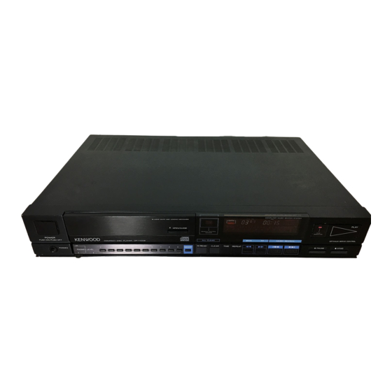
Photo is DP-1100B
•Refer to Parts List on page 177.
Photo is DP-110011
'Refer to Parts List on page 1 9 1 ,
Advertisement
Table of Contents


Need help?
Do you have a question about the DP-1100 B and is the answer not in the manual?
Questions and answers