Table of Contents
Advertisement
Quick Links
SERVICE MANUAL
2-LINE CORDLESS TELEPHONE WITH ANSWERING SYSTEM
SPECIFICATIONS
General
Frequency band
902 - 928 MHz
Operating channel
30 channels
Dial signal
Tone, 10 PPS (pulse) selectable
Supplied accessories
AC power adaptor (AC-T131)
Telephone line cords (3)
Wall bracket for base unit
Rechargeable battery pack (BP-T23)
Belt clip
Handset
Power source
Rechargeable battery pack BP-T23
Battery charging time
Approx. 12 hours
Battery life
Standby: Approx. 7 days
Talk:
Approx. 7 hours
Dimensions
Approx. 57 x 190 x 48 mm (w/h/d),
antenna excluded
1
1
15
(approx. 2
⁄
x 7
⁄
x 1
⁄
inches)
4
2
16
Antenna: Approx. 87 mm
1
(approx. 3
⁄
inches)
2
Mass
Approx. 268 g
(approx. 9.5 oz), battery included
SPP-A972
Base unit
Power source
DC 9V from AC power adaptor
AC-T131
Battery charging time
Approx. 24 hours
Dimensions
Approx. 185 x 70 x 225 mm (w/h/d),
antenna excluded
3
7
7
(approx. 7
⁄
x 2
⁄
x 8
⁄
inches)
8
8
8
Antenna: Approx. 150 mm
(approx. 6 inches)
Mass
Approx. 656 g
(approx. 1 lb 7 oz), wall bracket excluded
Answering machine
Maximum recording time
About 15 minutes, using incorporated IC
Greeting message
Up to 90 seconds per each
Incoming and Memo message
Up to 4 minutes per message
Design and specifications are subject to
change without notice.
US Model
Advertisement
Table of Contents

Related Manuals for Sony SPP-A972


Summary of Contents for Sony SPP-A972
- Page 1 SPP-A972 SERVICE MANUAL US Model SPECIFICATIONS General Base unit Frequency band Power source 902 - 928 MHz DC 9V from AC power adaptor Operating channel AC-T131 30 channels Battery charging time Dial signal Approx. 24 hours Tone, 10 PPS (pulse) selectable...
-
Page 2: Table Of Contents
LINE WITH MARK 0 ON THE SCHEMATIC DIAGRAMS AND IN THE PARTS LIST ARE CRITICAL TO SAFE OPERATION. REPLACE THESE COMPONENTS WITH SONY PARTS WHOSE PART NUMBERS APPEAR AS SHOWN IN THIS MANUAL OR IN SUPPLEMENTS PUB- LISHED BY SONY. -
Page 3: General
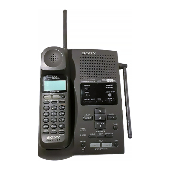
SECTION 1 This section is extracted from instruction manual. GENERAL Identifying the parts Refer to the pages indicated in parentheses for details. Base Unit 1 Message counter (p. 54, 75) 7 Battery compartment (p. 16) qg OFF button (p. 29) wf RINGER LEVEL switches (L1, L2) (p. -
Page 4: Setting Up The Base Unit
To L1/L1+L2 You can connect a computer or FAX, etc. to the and/or L2 DATA jack. AC power adaptor DATA jack SPP-A972 (supplied AC-T131) Notes To the • L2 jack is used for receiving or sending To DATA telephone outlets... -
Page 5: Preparing The Battery Pack
If the battery lasts only a few minutes even after 12 hours of charging, the usable life of the battery has expired and needs replacement. Contact your local Sony authorized dealer or service center, and ask Close the battery compartment for a Sony BP-T23 rechargeable battery pack. -
Page 6: Making Calls
Step 4: Entering the area code (continued) Select the number (”#1“ to ”#5“) to enter the local area code by turning Jog Dial. Enter three digits of your home area code using the dialing keys. Press Jog Dial. Press (PGM). ”ENTER AREA CODE“... -
Page 7: Receiving Calls
Making calls (continued) Making another call while talking If you have a spare battery Example: Making a call on line 2 while talking on line 1 You can replace the battery pack without disconnecting the call during Press (HOLD) while talking. a conversation. -
Page 8: Telephone Features
M t N t O t 6 • You may press Jog Dial instead of (PGM) in steps 4 and 6. Example: to enter “SONY”, press (7) P t Q t R t S t 7 four times (S), press (6) three times... -
Page 9: Setting The Ringer Type
• Alphabetical order: ABC...XYZ y symbols y * y # y 0 - 9 • Initial character: To search for “SONY” for example, press (7) and then turn Jog Dial to search through the names starting with P, Q, R, Press Jog Dial. -
Page 10: Switching The Phones During A Call
Switching the phones during a call Setting the ringer type (continued) You can easily switch between the handset and speakerphone on the Turning off the ringer of the handset base unit without disconnecting the call. The call on line 1 will be switched to line 1 on another phone and that on line 2 is switched to Perform steps 1 to 5 on page 37. -
Page 11: Transferring A Call
Transferring a call To transfer from the handset to the base unit You can transfer a call between the handset and base unit without disconnecting the call. Press (INTERCOM) to page the base unit. To transfer from the base unit to the handset The call is put on hold on the handset. -
Page 12: Answering Machine Features
Answering Machine Features Setting up the answering machine Having a conference call (continued) Setting the time and day of the week Switching conference from the handset to the base unit Press (MENU) repeatedly until Press (HOLD) on the handset to put both lines on hold. you hear “Set day and time”. -
Page 13: Setting The Number Of Rings
Setting up the answering machine (continued) Setting the audible message alert Setting the number of rings You have the option of having a beep to tell you if you have received any new incoming messages. You can select the number of times the phone rings before it answers to take a message. -
Page 14: Playing Back Messages
Playing back messages Adjusting the speaker volume If there are new messages, the display flashes the number of new To adjust the speaker volume, press messages. (VOLUME)(+) or (-). You will hear beeps if the audible message alert setting is on (see page 51). Message counter If the MAILBOX lamp flashes, press the mailbox button... -
Page 15: Caller Id Features
Operating from an outside phone Recording a memo message Setting the remote ID code (security code) You can leave messages for other users of the unit. To operate the answering machine from a touch-tone phone while you are away from home, you need to set the remote ID code (security Press (REC/MEMO). -
Page 16: Looking At The Caller Id List
Looking at the Caller ID list About the “*” mark The phone stores the data of the last 20 calls received including “OUT OF AREA” and “PRIVATE” calls. It keeps track of all calls received; “*” appears if there are more than two calls SMITH JOHN even if they were not answered. - Page 17 Using the Caller ID list (continued) To change the number of digits of the phone Storing a number of the Caller ID list into number the Phone Directory If the number of digits of the phone number in the Caller ID list is different from the actual phone number, you need to adjust the Display the name and phone number you want number of digits of the phone number to call back or store into the...
-
Page 18: Disassembly
SECTION 2 DISASSEMBLY Note: Follow the disassembly procedure in the numerical order given. CASE (REAR) 6 Remove the case (rear) in the direction of arrow B. 2 two screws (BVTP3 × 12) 1 Remove the “lid (hand), battery case” in the direction of arrow A. 5 claw 4 two claws 3 two claws... - Page 19 BASE (BOTTOM) 2 claw 1 five screws (BTP3 × 12) 3 base (bottom) 2 claw “ringer (SW), knob”, “knob, TP SW” S1001, S1002, S1003 NOTE: On installation BASE MAIN board, adjust to the S1001, S1002 and the S1003. BASE MAIN BOARD, RF UNIT (BASE) 1 three screws BASE MAIN board (BTP3 ×...
- Page 20 BASE KEY BOARD, SPEAKER (SP1) 1 four screws 2 plate, shield 6 eghit screws 9 BASE KEY board 4 bracket, SPK board 8 contact-C, B/S 5 speaker (SP1), “holder, speaker” 3 Remove two solders of lead. – 20 –...
-
Page 21: Electrical Adjustments
SECTION 3 ELECTRICAL ADJUSTMENTS ** FSK SEL is logic “1” (L1 FSK routed to External CID & L2 FSK BASE UNIT routed to ASIC) in the “Base Unit on L1, L2 Idle” condition. FSK SEL is logic “0” (L2 FSK routed to External CID & L1 FSK 1. -
Page 22: Handset
HANDSET 1. Test Mode 2. Adjustment Equipment and Connection [Entering the Test Mode] frequency counter [PGM] 1. Press the key, then displayed “DIRECTORY AREA RINGER” on the LCD. 2. Press the keys, then displayed on – the LCD as below. –... - Page 23 • Frequency Allocation Tables The RF channels for the SPP-A972 are allocated in fixed pairs as indicated in the tables below. The duplex frequency is maintained at 22.75 MHz for 19 of the 30 channels and 17.95 MHz for the remaining 11 channels.
-
Page 24: Diagrams
SPP-A972 SECTION 4 DIAGRAMS 4-1. BLOCK DIAGRAM – MAIN Section – CONF, INT COM, LINE SPK2, SPK1, L2, L1 SELECT (Page 27) U1001 (1/4) CONF ANT1 (ANTENNA) TX DATA TX DATA LINE SELECT U1004 (3/4) RX AUDIO DSIN AF AMP... -
Page 25: Block Diagram - Display/Key Shift/Power Supply Section
SPP-A972 4-2. BLOCK DIAGRAM – DISPLAY/KEY SHIFT/POWER SUPPLY Section – MAIL BOX MAIL BOX MAIL BOX Ref No. PANEL DESIGNATION Ref No. PANEL DESIGNATION B+ SWITCH TAD TARM REC/MEMO SKIP/QUICK P1.7 (FOR LEDS) S DATA ERASE MAIL BOX 1 TAD CTR... -
Page 26: Block Diagram - Handset Section
SPP-A972 4-3. BLOCK DIAGRAM – HANDSET Section – ANT2 (ANTENNA) RX PWR B+ RX PWR U1005 RX AUDIO DSIN (SPEAKER) TX PWR B+ BUZZER DRIVE U1002 RINGER Q1009 (BUZZER) TX PWR U1003 TX DATA TXDATA (MIC) RF UNIT B+ SWITCH... -
Page 27: Note For Printed Wiring Boards And Schematic Diagrams
4-4. NOTE FOR PRINTED WIRING BOARDS AND SCHEMATIC DIAGRAMS Note on Printed Wiring Board: Note on Schematic Diagram: • X : parts extracted from the component side. • All capacitors are in µF unless otherwise noted. pF: µµF • Y : parts extracted from the conductor side. 50 WV or less are not indicated except for electrolytics •... -
Page 28: Base Main Board (Component Side)
• Waveforms – BASE MAIN Board – – HAND MAIN Board – 1 U1014 qa (XOUT) 3 U1001 rl (XTAL1) IV/DIV, 100 ns/DIV 400 mV/DIV, 20 ns/DIV 820 mVp-p 2.8 Vp-p 279 ns 54.3 ns 2 U1000 rl (XTAL1) 400 mV/DIV, 20 ns/DIV 820 mVp-p 54.3 ns –... - Page 29 SPP-A972 4-5. PRINTED WIRING BOARD – BASE MAIN Board (Component Side) – • Semiconductor Location BASE MAIN BOARD (COMPONENT SIDE) Ref. No. Location D1010 C1056 D1000 I-10 D1002 D1003 H-11 R1171 Q1008 Q1009 R1180 R1165 D1007 R1153 C1129 R1181 D1008...
-
Page 30: Printed Wiring Board - Base Main Board (Conductor Side)
SPP-A972 4-6. PRINTED WIRING BOARD – BASE MAIN Board (Conductor Side) – • Semiconductor Location BASE MAIN BOARD (CONDUCTOR SIDE) Ref. No. Location J1008 DATA D1004 D1005 D1006 J1018 D1011 T1000 D1014 LINE D1016 TRANSFORMER D1021 D1017 C1084 D1018 D1017... -
Page 31: Schematic Diagram – Base Main Board (1/3)
SPP-A972 4-7. SCHEMATIC DIAGRAM – BASE MAIN Board (1/3) – • See page 49 for IC Block Diagram. (Page 41) (Page 39) – 37 – – 38 –... -
Page 32: Schematic Diagram – Base Main Board (2/3)
SPP-A972 4-8. SCHEMATIC DIAGRAM – BASE MAIN Board (2/3) – • See page 32 for Waveform. • See page 49 for IC Block Diagrams. (Page 41) (Page 38) – 39 – – 40 –... -
Page 33: Schematic Diagram – Base Main Board (3/3)
SPP-A972 4-9. SCHEMATIC DIAGRAM – BASE MAIN Board (3/3) – • See page 32 for Waveform. • See page 50 for IC Block Diagram. (Page 38) (Page 40) (Page 44) (Page 44) – 41 – – 42 –... -
Page 34: 4-10. Printed Wiring Board - Base Key Board
4-10. PRINTED WIRING BOARD – BASE KEY Board – • Semiconductor Location Ref. No. Location BASE KEY BOARD B C E E C B E C B NEW CALL REC/MEMO MESSAGE COUNTER D3, S3 ERASE ANSWER ON/OFF TIME/SET SELECT MENU –... -
Page 35: Schematic Diagram - Base Key Board
SPP-A972 4-11. SCHEMATIC DIAGRAM – BASE KEY Board – • See page 51 for IC Block Diagram. (Page 42) (Page 42) – 44 –... -
Page 36: 4-12. Printed Wiring Board - Hand Main Board
SPP-A972 4-12. PRINTED WIRING BOARD – HAND MAIN Board – • Semiconductor Location HAND MAIN BOARD (COMPONENT SIDE) Ref. No. Location D1001 D-12 D1002 B-12 D1003 E-11 C1055 D1004 D-12 U1005 R1079 C1021 3 2 1 D1006 C-12 C1048 –... -
Page 37: Schematic Diagram - Hand Main Board
SPP-A972 4-13. SCHEMATIC DIAGRAM – HAND MAIN Board – • See page 32 for Waveform. • See page 51 for IC Block Diagram. – 47 – – 48 –... - Page 38 • IC Block Diagrams – BASE MAIN Board – U1013 U4083B U1002, 1028 MC74HC4053DTR2 15 14 BIAS CIRCUIT U1012, 1020, 1021 SN74HC595ADB-E05 SHIFT REGISTER LATCH PARALLEL DATA OUTPUT – 49 –...
- Page 39 U1015 ILC7081AIM5-30 U1014 PCC317 TRANS- ERROR ALERT SIGNAL CONDUCTANCE BANDGAP HIGH TONE REFERENCE – IN– VOUT FILTER VREF TONE DETECTION ST/GT ALGORITHM ALERT SIGNAL INTERNAL LOW TONE ANTI-ALIAS FILTER GUARD CNOISE FILTER TIME ON/OFF BIAS VREF GENERATOR INTERRUPT GENERATOR TRIGIN CARRIER DETECTOR TRIGRC...
- Page 40 U1019 U4082B VREF ATTEN- DIAL UATOR TONE DETECTOR BACKGROUND BACKGROUND LEVEL LEVEL NOISE NOISE DETECTOR DETECTOR DETECTOR DETECTOR LEVEL COMPARATOR COMPARATOR LEVEL DETECTOR DETECTOR HYBRID HYBRID ATTENUATOR AMP 2 AMP 1 FILTER – – – – HAND MAIN Board – –...
-
Page 41: Exploded Views
SECTION 5 EXPLODED VIEWS NOTE: • -XX and -X mean standardized parts, so they • Items marked “*” are not stocked since they may have some difference from the original are seldom required for routine service. Some one. delay should be anticipated when ordering •... - Page 42 (2) BASE SET SECTION ANT1 (Including A) supplied not supplied supplied supplied Ref. No. Part No. Description Remark Ref. No. Part No. Description Remark 3-041-534-01 FOOT, RUBBER 3-039-826-01 BASE (1), BUTTON 3-039-825-01 BASE (BOTTOM) 3-039-818-01 BASE (2), BUTTON 3-041-211-01 RUBBER, MIC 1-678-979-11 BASE KEY BOARD 3-041-523-01 RINGER (SW), KNOB 4-356-741-21 SCREW TAPPING (BIND 2X8)
-
Page 43: Electrical Parts List
BASE KEY SECTION 6 BASE MAIN ELECTRICAL PARTS LIST NOTE: • Due to standardization, replacements in the • Items marked “*” are not stocked since they The components identified by mark 0 or dotted line with mark are seldom required for routine service. parts list may be different from the parts speci- 0 are critical for safety. - Page 44 BASE MAIN Ref. No. Part No. Description Remark Ref. No. Part No. Description Remark C1036 1-162-970-11 CERAMIC CHIP 0.01uF C1102 1-107-826-11 CERAMIC CHIP 0.1uF C1037 1-162-964-11 CERAMIC CHIP 0.001uF C1103 1-162-927-11 CERAMIC CHIP 100P C1104 1-162-965-11 CERAMIC CHIP 0.0015uF 10% C1038 1-124-233-11 ELECT 10uF...
- Page 45 BASE MAIN Ref. No. Part No. Description Remark Ref. No. Part No. Description Remark C1200 1-102-106-00 CERAMIC 100PF Q1008 8-729-026-07 TRANSISTOR MMBT3906LT1 C1201 1-102-106-00 CERAMIC 100PF Q1009 8-729-026-07 TRANSISTOR MMBT3906LT1 C1202 1-102-106-00 CERAMIC 100PF Q1010 T-941-615-31 TRANSISTOR MMBT3904LT1 C1204 1-102-106-00 CERAMIC 100PF Q1012 T-941-615-31 TRANSISTOR MMBT3904LT1...
- Page 46 BASE MAIN Ref. No. Part No. Description Remark Ref. No. Part No. Description Remark R1060 1-216-833-11 RES, CHIP 1/16W R1126 1-216-833-11 RES, CHIP 1/16W R1061 1-216-833-11 RES, CHIP 1/16W R1127 1-216-858-11 RES, CHIP 1.2M 1/16W R1062 1-216-833-11 RES, CHIP 1/16W R1128 1-216-852-11 RES, CHIP 390K...
- Page 47 BASE MAIN HAND MAIN Ref. No. Part No. Description Remark Ref. No. Part No. Description Remark U1021 8-759-268-32 IC SN74HC595ADB-E05 R1195 1-216-864-11 METAL CHIP 1/16W U1022 8-719-018-89 PHOTO COUPLER LTV817-C R1203 1-218-462-11 METAL FILM 1/4W U1023 8-719-018-89 PHOTO COUPLER LTV817-C R1204 1-218-462-11 METAL FILM 1/4W...
- Page 48 HAND MAIN Ref. No. Part No. Description Remark Ref. No. Part No. Description Remark C1053 1-162-964-11 CERAMIC CHIP 0.001uF R1004 1-216-853-11 METAL CHIP 470K 1/16W C1055 1-164-346-11 CERAMIC CHIP R1008 1-216-818-11 METAL CHIP 1/16W C1056 1-164-346-11 CERAMIC CHIP R1009 1-216-804-11 METAL CHIP 1/16W C1062 1-110-563-11 CERAMIC CHIP...
- Page 49 SPP-A972 HAND MAIN Ref. No. Part No. Description Remark Ref. No. Part No. Description Remark < ROTARY ENCODER/SWITCH > S1002 1-475-568-12 ENCODER, ROTARY (JOG) S1003 1-771-833-11 SWITCH, SLIDE (VOL) < BUZZER/MIC/SPEAKER/IC > U1001 A-3649-041-A ASIC ASSY, HAND U1002 1-505-594-11 BUZZER...
Need help?
Do you have a question about the SPP-A972 and is the answer not in the manual?
Questions and answers