Sony SPP-A946 Service Manual
Cordless telephone with ansering system
Hide thumbs
Also See for SPP-A946:
- Operating instructions manual (112 pages) ,
- Operating instructions manual (112 pages)

Related Manuals for Sony SPP-A946


Summary of Contents for Sony SPP-A946
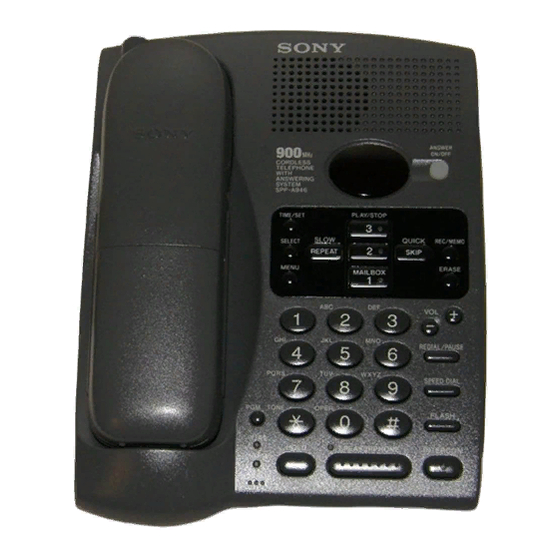
- Page 1 SPP-A946/A947 SERVICE MANUAL US Model SPP-A946 Ver 1.0 2000. 02 Canadian Model SPP-A947 SPECIFICATIONS CORDLESS TELEPHONE WITH ANSERING SYSTEM MICROFILM...
-
Page 2: Table Of Contents
SONY PARTS WHOSE PART NUMBERS APPEAR AS DE FONCTIONNEMENT. NE REMPLACER CES COM- SHOWN IN THIS MANUAL OR IN SUPPLEMENTS PUB- POSANTS QUE PAR DES PIÈCES SONY DONT LES LISHED BY SONY. NUMÉROS SONT DONNÉS DANS CE MANUEL OU DANS LES SUPPLÉMENTS PUBLIÉS PAR SONY. - Page 3 SECTION 1 This section is extracted from instruction manual. GENERAL – 3 –...
- Page 4 – 4 –...
- Page 5 – 5 –...
- Page 6 – 6 –...
- Page 7 – 7 –...
- Page 8 – 8 –...
- Page 9 – 9 –...
- Page 10 – 10 –...
- Page 11 – 11 –...
- Page 12 – 12 –...
-
Page 13: Disassembly
SECTION 2 DISASSEMBLY Note: Follow the disassembly procedure in the numerical order given. HAND CABINET (REAR) 5 Remove the hand cabinet (rear) in the direction of arrow B. 3 two claws 4 claw 2 two screws (BTP3 × 12) 1 Remove the battery case lid in the direction of arrow A. - Page 14 CABINET (LOWER) ASSY 2 three claws 1 four screws (BTP2.6 × 12) 3 cabinet (lower) assy BASE KEY BOARD, SPEAKER (SP701) 1 ten screws 4 holder (SP) (BTP2.6 × 8) 3 two screws (BTP2.6 × 8) 5 speaker (SP701) 2 BASE KEY board –...
- Page 15 BASE MAIN BOARD 1 flat cable 2 seven screws (BTP2.6 × 8) 2 four screws (BTP2.6 × 8) 5 two screws (BTP2.6 × 8) 3 spring washer 6 BASE MIC board 4 BASE MAIN board – 15 –...
-
Page 16: Test Mode
SECTION 3 TEST MODE BASE UNIT – MAIN Section – [Setting the Test Mode] [INTERCOM] 1. Power on with pressing the key for five seconds. 2. When the test mode is set, it beeps confirm tone and CHARGE LED turns on for 50 msec. [TONE] [DIAL MODE] Note: If setting the test mode with the status that... - Page 17 [Test Mode Execution] [INTERCOM] Press the key to execute any of the following tests: Test Mode Step Name VCO/TX FREQ. ADJ TX MOD CHECK TX DATA RX SENS SQ SENS BELL CHECK L/IN DTMF DUAL TONE DATA IN CHECK CHARGE CHECK DUPLEX INTERCOM DTMF SINGLE TONE...
- Page 18 – DSP Section – [Setting the DSP Test Mode] [ANSWER ON/OFF] 1. Power on with pressing the key for 3 seconds. 2. When the DSP test mode (step 1) is set, it beeps confirm tone. [Releasing the DSP Test Mode] To release the test mode, perform as follows: •...
- Page 19 4. STEP 4 When set to this step, it indicates “ 4” on the 7 segments LED (D217), and keep beeps DTMF tone. [SLOW, REPEAT] Each time the key is pressed, DTMF tone is change. 5. STEP 5 When set to this step, the 7 segments LED (D217) goes off. In this step, it will be recording mode from line input (LINE jack: J1) every time.
-
Page 20: Handset
HANDSET [Setting the Test Mode] 1. Power on with press the key and the key simultaneously for one second. 2. It beeps confirm tone, and the test mode is set. [PGM] Note: If the key is pressed, the unit cold starts next time when the power is turned on. [Releasing the Test Mode] To release the test mode, perform as follows: [TALK]... -
Page 21: Electrical Adjustments
SECTION 4 ELECTRICAL ADJUSTMENTS – RX Adjustments – 0 dBm = 0.775 V, 0 dBV = 1 V BASE UNIT DISCRI Voltage Adjustment Setting: • Make the set in test mode. (See page 16) • Remove the solder of the BP (ANT) on the BASE MAIN board when performing adjustments. - Page 22 3. SQ Sensitivity Adjustment Setting: TP (ANT) TP (GND) Carrier frequency: 902.902467 MHz Modulation: no modulation Output level: –114 dBm Procedure: 1. Change the modulation to no modulation and change the out- put level of SSG to –114 dBm. [INTERCOM] 2.
-
Page 23: Handset
– RX Adjustments – HANDSET 1. DISCRI Voltage Adjustment • Make the set in test mode. (See page 20) Setting: • Remove the solder of the BP (ANT) on the HAND MAIN board when performing adjustments. After completing the adjustments, short the BP (ANT) by solder. - Page 24 3. SQ Sensitivity Adjustment Setting: TP (ANT) TP (GND) Carrier frequency: 926.997467 MHz Modulation: 1 kHz, ±8 kHz deviation Output level: –113 dBm Procedure: 1. Change the output level of SSG to –113 dBm. 2. Press the key to change the test mode step to SQ SENS. 3.
-
Page 25: Diagrams
SPP-A946/A947 SECTION 5 DIAGRAMS 5-1. BLOCK DIAGRAM – BASE UNIT Section (1/2) – B+ (3V) DISCRI VOLTAGE 2nd MIXER, LIMITER AMP, DET, 1st MIXER, VCO, PLL SYNTHESIZER AF AMP, SQUELCH CONTROL ANT701 IC302 EXPANDER, COMPRESSOR (ANTENNA) OUT LEVEL QUAD COIL 10.555MHz... - Page 26 SPP-A946/A947 5-2. BLOCK DIAGRAM – BASE UNIT Section (2/2) – LINE TRANSFORMER LINE AF AMP TX LINE MUTE HYBRID AMP (Page 26) IC4 (1/2) BUFFER RX LINE MUTE AF AMP (Page 26) IC6 (1/2) IC4 (2/2) BUFFER IC6 (2/2) IC202...
-
Page 27: Block Diagram - Handset Section
SPP-A946/A947 5-3. BLOCK DIAGRAM – HANDSET Section – L602 B+ (3V) DISCRI VOLTAGE 2nd MIXER, LIMITER AMP, DET, 1st MIXER, VCO, PLL SYNTHESIZER AF AMP, SQUELCH CONTROL RT602 IC502 EXPANDER, COMPRESSOR IC601 SPEAKER IC602 OUT LEVEL QUAD COIL FT601 FT602 10.555MHz... -
Page 28: Note For Printed Wiring Boards And Schematic Diagrams
SPP-A946/A947 5-5. PRINTED WIRING BOARD – BASE RF Section – 5-4. NOTE FOR PRINTED WIRING BOARDS AND SCHEMATIC DIAGRAMS Note on Printed Wiring Board: Note on Schematic Diagram: • X : parts extracted from the component side. • All capacitors are in µF unless otherwise noted. pF: µµF •... - Page 29 SPP-A946/A947 5-6. SCHEMATIC DIAGRAM – BASE RF Section – • See page 52 for IC Block Diagram. (Page 37) (Page 37) (Page 37) – 33 – – 34 –...
-
Page 30: Printed Wiring Boards - Base Main Section
SPP-A946/A947 5-7. PRINTED WIRING BOARDS – BASE MAIN Section – • Semiconductor Location – RINGER DIAL MODE BASE MAIN BOARD DC IN 9V OFF , L , H PULSE < TONE Ref. No. Location 5 3 1 2 4 6... - Page 31 SPP-A946/A947 5-8. SCHEMATIC DIAGRAM – BASE MAIN Section – • See page 43 for Waveforms. • See page 51 for IC Block Diagrams. (Page 34) (Page 33) (Page 34) (Page 41) – 37 – – 38 –...
-
Page 32: Printed Wiring Board - Base Key Section
SPP-A946/A947 5-9. PRINTED WIRING BOARD – BASE KEY Section – • Semiconductor Location BASE KEY BOARD (CONDUCTOR SIDE) Ref. No. Location D201 B-11 SP701 D202 B-12 (ANTENNA) C209 D203 D-12 BASE KEY BOARD D217 D204 B-11 (COMPONENT SIDE) D213, S216... -
Page 33: Schematic Diagram - Base Key Section
SPP-A946/A947 5-10. SCHEMATIC DIAGRAM – BASE KEY Section – • See page 43 for Waveform. • See page 51 for IC Block Diagrams. (Page 38) – 41 – – 42 –... -
Page 34: Printed Wiring Board - Hand Rf Section
SPP-A946/A947 5-11. PRINTED WIRING BOARD – HAND RF Section – • Waveforms – BASE MAIN Board – – BASE KEY Board – – HAND MAIN Board – 1 IC3 1 (OSC1) 3 IC202 tf (XIN) 4 IC601 1 (OSC1) HAND RF BOARD... -
Page 35: Schematic Diagram - Hand Rf Section
SPP-A946/A947 5-12. SCHEMATIC DIAGRAM – HAND RF Section – (Page 49) (Page 49) (Page 49) – 45 – – 46 –... -
Page 36: Printed Wiring Board - Hand Main Section
SPP-A946/A947 5-13. PRINTED WIRING BOARD – HAND MAIN Section – • Semiconductor Location Ref. No. Location D601 D602 HAND MAIN BOARD (COMPONENT SIDE) SP801 D603 C-12 (SPEAKER) D604 C-12 D605 C-11 D606 D-10 D601 D607 (A947) D608 D609 B C E... -
Page 37: Schematic Diagram - Hand Main Section
SPP-A946/A947 5-14. SCHEMATIC DIAGRAM – HAND MAIN Section – • See page 43 for Waveforms. • See page 51 for IC Block Diagrams. (Page 46) (Page 45) (Page 46) – 49 – – 50 –... - Page 38 • IC Block Diagrams IC302 M64884FP-C60J (BASE RF Board) IC502 M64884FP-C60J (BASE RF Board) IC1 IR3N74AN (BASE MAIN Board) IC602 IR3N74AN (HAND MAIN Board) 16 15 VCO (RX) LOCK VREF VREF DETECTOR ∆G – – MUTE LIMITER PHASE PULSE VREF DETECTOR COUNTER –...
-
Page 39: Ic Pin Function Description
5-15. IC PIN FUNCTION DESCRIPTION • BASE MAIN BOARD IC8 MB89174APF-G-288-BND (SYSTEM CONTROLLER) Pin No. Pin Name Description DTMF DTMF tone signal output terminal System reset signal input from the reset signal generator (Q18) “L”: reset RESET For several hundreds msec. after the power supply rises, “L” is input, then it changes to “H” 3, 4 MOD0, MOD1 Setting terminal for the CPU operational mode Fixed at “L”... - Page 40 Pin No. Pin Name Description — Ground terminal DATA EN Transmit data enable signal output terminal INT LED LED drive signal output of the INTERCOM indicator (D210) “L”: LED on CHG LED LED drive signal output of the CHARGE indicator (D209) “L”: LED on RING VOL Bell volume control terminal “L”: bell volume is low LINE MUTE...
- Page 41 • BASE KEY BOARD IC202 D16559UAC11AQC (DSP) Pin No. Pin Name Description SP LED LED drive signal output of the SPEAKERPHONE indicator (D211) “L”: LED on TBUSY Busy signal output to the system controller (IC8) “H”: in the midst dialing 3 to 5 ENB1 to ENB3 Telephone mode signal output to the system controller (IC8)
- Page 42 Pin No. Pin Name Description Microphone output from the internal operational amplifier VREF Reference voltage output terminal PLLGND — Ground terminal (for PLL) PLLVCC — Power supply terminal (+5V) (for PLL) PLLVCC — Power supply terminal (+5V) (for PLL) XOUT System clock output terminal (4.081408 MHz) System clock input terminal (4.081408 MHz) DGND...
- Page 43 • HAND MAIN BOARD IC603 MB89174LPF-G-289-BND (SYSTEM CONTROLLER) Pin No. Pin Name Description Not used (open) System reset signal input from the reset signal generator (Q615) “L”: reset RESET For several hundreds msec. after the power supply rises, “L” is input, then it changes to “H” 3, 4 MOD0, MOD1 Setting terminal for the CPU operational mode Fixed at “L”...
-
Page 44: Exploded Views
SECTION 6 EXPLODED VIEWS NOTE: • -XX and -X mean standardized parts, so they • Items marked “*” are not stocked since they may have some difference from the original are seldom required for routine service. Some one. delay should be anticipated when ordering •... - Page 45 (2) BASE UNIT SECTION SP701 supplied supplied (BASE MIC board, complete) supplied supplied supplied D217 not supplied AT701 (Including A) Ref. No. Part No. Description Remark Ref. No. Part No. Description Remark 3-043-638-01 CUSHION 3-036-336-01 HOOK * 52 A-3672-931-A BASE KEY BOARD, COMPLETE * 63 A-3672-930-A BASE MAIN BOARD, COMPLETE 1-771-869-11 SWITCH, RUBBER KEY (BASE 12 KEY)
-
Page 46: Electrical Parts List
SECTION 7 BASE KEY ELECTRICAL PARTS LIST NOTE: • Due to standardization, replacements in the • Items marked “*” are not stocked since they The components identified by mark 0 or dotted line with mark are seldom required for routine service. parts list may be different from the parts speci- 0 are critical for safety. - Page 47 BASE KEY Ref. No. Part No. Description Remark Ref. No. Part No. Description Remark IC203 8-759-583-75 IC KM29W040AT R222 1-216-821-11 METAL CHIP 1/16W IC204 8-759-235-99 IC TC74HC132AF (EL) R223 1-216-821-11 METAL CHIP 1/16W IC206 1-781-631-11 FILTER, SAW R224 1-216-821-11 METAL CHIP 1/16W R225 1-216-821-11 METAL CHIP...
- Page 48 BASE KEY BASE MAIN Ref. No. Part No. Description Remark Ref. No. Part No. Description Remark R284 1-216-821-11 METAL CHIP 1/16W 1-107-826-11 CERAMIC CHIP 0.1uF R285 1-216-821-11 METAL CHIP 1/16W 1-162-964-11 CERAMIC CHIP 0.001uF R286 1-216-821-11 METAL CHIP 1/16W 1-107-826-11 CERAMIC CHIP 0.1uF R287 1-216-827-11 METAL CHIP...
- Page 49 BASE MAIN Ref. No. Part No. Description Remark Ref. No. Part No. Description Remark 1-162-970-11 CERAMIC CHIP 0.01uF 1-162-920-11 CERAMIC CHIP 27PF 8-719-055-76 DIODE 1N4148 1-162-920-11 CERAMIC CHIP 27PF 8-719-109-71 DIODE RD3.9ES-B1 1-104-665-11 ELECT 100uF 8-719-055-76 DIODE 1N4148 8-719-055-76 DIODE 1N4148 1-162-970-11 CERAMIC CHIP 0.01uF 8-719-910-68 DIODE HZ6C2L...
- Page 50 BASE MAIN Ref. No. Part No. Description Remark Ref. No. Part No. Description Remark 8-729-216-22 TRANSISTOR 2SA1162-G 8-729-120-28 TRANSISTOR 2SC1623-L5L6 1-216-841-11 METAL CHIP 1/16W 8-729-216-22 TRANSISTOR 2SA1162-G 1-216-833-11 RES-CHIP 1/16W 8-729-120-28 TRANSISTOR 2SC1623-L5L6 1-216-021-00 METAL CHIP 1/10W 1-216-848-11 METAL CHIP 180K 1/16W 8-729-216-22 TRANSISTOR...
- Page 51 BASE MAIN BASE MIC BASE RF Ref. No. Part No. Description Remark Ref. No. Part No. Description Remark R102 1-216-851-11 METAL CHIP 330K 1/16W R168 1-216-845-11 METAL CHIP 100K 1/16W R103 1-216-845-11 METAL CHIP 100K 1/16W R169 1-216-821-11 METAL CHIP 1/16W R104 1-216-833-11 RES-CHIP...
- Page 52 BASE RF Ref. No. Part No. Description Remark Ref. No. Part No. Description Remark C319 1-162-921-11 CERAMIC CHIP 33PF < DIODE > C320 1-162-964-11 CERAMIC CHIP 0.001uF D302 8-719-076-89 DIODE 1SV270 (TPH3) C321 1-162-921-11 CERAMIC CHIP 33PF D303 8-719-076-90 DIODE 1SV314 C323 1-162-910-11 CERAMIC CHIP 0.25PF 50V...
- Page 53 BASE RF HAND MAIN Ref. No. Part No. Description Remark Ref. No. Part No. Description Remark R351 1-216-809-11 METAL CHIP 1/16W C645 1-127-573-11 CERAMIC CHIP R352 1-216-797-11 METAL CHIP 1/16W C647 1-107-826-11 CERAMIC CHIP 0.1uF R353 1-216-840-11 METAL CHIP 1/16W C648 1-162-907-11 CERAMIC CHIP 0.25PF 50V...
- Page 54 HAND MAIN Ref. No. Part No. Description Remark Ref. No. Part No. Description Remark < JACK > R622 1-216-821-11 METAL CHIP 1/16W J602 1-573-753-11 JACK R624 1-216-809-11 METAL CHIP 1/16W R625 1-216-809-11 METAL CHIP 1/16W < RESISTOR > R626 1-216-825-11 METAL CHIP 2.2K 1/16W R627...
- Page 55 HAND MAIN HAND RF Ref. No. Part No. Description Remark Ref. No. Part No. Description Remark C540 1-162-921-11 CERAMIC CHIP 33PF R688 1-216-178-00 RES-CHIP 1/8W C541 1-162-909-11 CERAMIC CHIP 0.25PF 50V (A947) R689 1-216-821-11 METAL CHIP 1/16W C542 1-162-908-11 CERAMIC CHIP 0.25PF 50V (A947) C543...
- Page 56 SPP-A946/A947 HAND RF Ref. No. Part No. Description Remark Ref. No. Part No. Description Remark < COIL > MISCELLANEOUS ************** L501 1-403-663-41 INDUCTOR 22nH L502 1-403-657-11 INDUCTOR 6.8nH 1-771-870-11 SWITCH, RUBBER KEY (HAND 12 KEY) (A946) L503 1-403-661-11 INDUCTOR 15nH...
Need help?
Do you have a question about the SPP-A946 and is the answer not in the manual?
Questions and answers