Advertisement
Quick Links
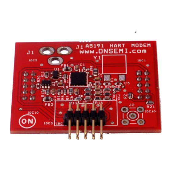
A5191HRTNGEVB
A5191HRTNGEVB
Evaluation Board User's
Manual
Introduction
The A5191HRTNGEVB evaluation board includes all
external
components
needed
A5191HRT IC and demonstrates the small PCB surface area
such an implementation requires. The EVB allows easy
design of HART® implementations using A5191HRT.
Overview
The A5191HRT is a single−chip, CMOS modem for use
in highway addressable remote transducer (HART) field
instruments and masters. The modem and a few external
passive components provide all of the functions needed to
satisfy HART physical layer requirements including
modulation, demodulation, receive filtering, carrier detect,
and transmit−signal shaping.
The A5191HRT uses phase continuous frequency shift
keying (FSK) at 1200 bits per second. To conserve power the
receive circuits are disabled during transmit operations and
vice versa. This provides the half−duplex operation used in
HART communications.
© Semiconductor Components Industries, LLC, 2016
July, 2016 − Rev. 5
for
operating
the
Figure 1. A5191HRTNGEVB Evaluation Board
1
www.onsemi.com
EVAL BOARD USER'S MANUAL
Features
•
Single−chip, Half−duplex 1200 Bits per Second FSK
Modem
•
Bell 202 Shift Frequencies of 1200 Hz and 2200 Hz
•
3.0 V − 5.5 V Power Supply
•
Transmit−signal Wave Shaping
•
Receive Band−pass Filter
•
Low Power: Optimal for Intrinsically Safe Applications
•
Compatible with 3.3 V or 5 V Microcontroller
•
Internal Oscillator Requires 460.8 kHz Crystal or
Ceramic Resonator
•
Meets HART Physical Layer Requirements
•
Industrial Temperature Range of −40°C to +85°C
•
Available in 28−pin PLCC, 32−pin QFN and 32−pin
LQFP Packages
Applications
•
HART Multiplexers
•
HART Modem Interfaces
•
4 – 20 mA Loop Powered Transmitters
Publication Order Number:
EVBUM2130/D
Advertisement

Related Manuals for ON Semiconductor A5191HRTNGEVB


Summary of Contents for ON Semiconductor A5191HRTNGEVB
- Page 1 A5191HRTNGEVB Evaluation Board User's Manual www.onsemi.com EVAL BOARD USER’S MANUAL Introduction Features • The A5191HRTNGEVB evaluation board includes all Single−chip, Half−duplex 1200 Bits per Second FSK external components needed operating Modem • A5191HRT IC and demonstrates the small PCB surface area Bell 202 Shift Frequencies of 1200 Hz and 2200 Hz such an implementation requires.
-
Page 2: Electrical Characteristics
A5191HRTNGEVB ELECTRICAL CHARACTERISTICS Table 1. ELECTRICAL CHARACTERISTICS OF THE A5191HRTNGEVB BOARD Value Symbol Parameter / Condition Unit Supply voltage 2.78 6.00 CURRENT CONSUMPTION = 2.78V, idle = 3.00 V, idle = 6.00V, idle External clock, V = 3.00 V, idle TRANSMITTED FREQUENCY Mark “1”... - Page 3 A5191HRTNGEVB A5191HRTNGEVB DESCRIPTION Schematic Diagram Figure 2. Schematic of A5191HRTNEVB www.onsemi.com...
- Page 4 ON Semiconductor 460.8 kHz ECS Crystal ZTBF−460.8−E General Overview The A5191HRTNGEVB evaluation board demonstrates alternatives. A drawing of the board where the different the external components required for the operation of the IC. sections are indicated is shown below. We will cover the different sections below as well as possible Figure 3.
- Page 5 Power Supply and References Power Supply Figure 4. Supply Voltage and Power on Reset The A5191HRTNGEVB is designed for a nominal Current consumption of the module is very limited, voltage of 3 V. However, A5191HRT can be operated up to making it ideal to be battery or loop−powered.
- Page 6 The CDREF through the band−pass receive filter. The ideal value for the reference voltage on the A5191HRTNGEVB is generated AREF reference voltage depends on the voltage supply, and by a resistor division of the AREF reference. This will create is chosen roughly half−way the operating range of the...
- Page 7 Value approximately 2.5 mA. A bias resistor of 499 kW is used on AREF reference voltage 1.212 V the A5191HRTNGEVB. For low cost solutions, a 470 kW is acceptable with minimal effect on operation. CDREF reference voltage 1.128 V 22 mA Current through R Figure 6.
- Page 8 A5191HRTNGEVB Microcontroller Interface IDC1 RESET PC20110513 .4 Figure 8. Microcontroller Interface Table 5. MICROCONTROLLER INTERFACE Pin Number Signal Type Description Open drain Reset signal from the voltage supervisor, open drain with pull−up Output Carrier Detect Input Receive from microcontroller Output...
- Page 9 A5191HRTNGEVB Figure 9. Clock Skew Even if your own time base is perfect, you still must plan can only drive impedances higher than 30 kW, and as a on a possible 35% shift in a bit boundary, since you don’t consequence may need to be amplified to drive low have control over time bases in other HART devices.
- Page 10 The receive band pass filter is implemented on the minimal changes to the filter characteristic. This A5191HRTNGEVB. The values are listed in Table 6 and the implementation will have a slightly reduced gain in the pass filter schematic is displayed in Figure 12. For cost purposes, band.
- Page 11 A5191HRTNGEVB Table 6. RECEIVE FILTER COMPONENT VALUES Value E12 (Low−cost) Reference Value E96 215 kW 1% 220 kW 1% 215 kW 1% 220 kW 1% 499 kW 1% 470 kW 1% 787 kW 1% 680 kW 1% 422 kW 1%...
- Page 12 A5191HRTNGEVB Figure 14. Monte Carlo Analysis of the First Filter Stage for 10% (above) and 1% (below) Accuracy In Figure 15 the measured filter characteristic of both too high in frequency to have an influence on the phase of variations are shown next to a simulated result. These HART signals.
- Page 13 A5191HRTNGEVB Figure 16. Group Delay of the Total Filter First Stage the operational amplifier, and the removal of R . The filter The first stage of the filter is implemented as a modified is a variation on the Sallen−Key topology with three poles.
- Page 14 A5191HRTNGEVB The transfer function of this type of filter is: Introducing R does not introduce another pole or zero but changes the denominator of the transfer function, and thus the location of the poles. The final transfer function of the first filter stage is thus a...
-
Page 15: Application Ideas
A5191HRTNGEVB Figure 20. Characteristic of the Second Stage of the Filter APPLICATION IDEAS The A5191HRT takes care of the HART modulation. This Next, the values of R and R are chosen depending on the HART signal must then be superimposed on a 4−20mA most significant bit of the DAC. - Page 16 Figure 22. To use this schematic, the coupling capacitor resistor used, some gain or attenuation may be required to C4 on the A5191HRTNGEVB will need to be replaced by get a 1 mA peak−to−peak HART output signal. This can be a 0 W resistor, or new biasing must be provided.
- Page 17 A5191HRTNGEVB nRTS Loop + AREF Loop − Figure 22. Sample Master Implementation APPENDIX Calculation of a three Pole Sallen−Key High Pass Filter The first stage of the receive filter uses a three pole active Resistors R and R serve only to bias the amplifier...
- Page 18 A5191HRTNGEVB Equation 6 simplifies to: (eq. 7) Substituting V1 and V2 in Equation 7 using Equations 4 and 5, and simplifying we find the transfer function: Where: Adding the compensation capacitor on the operational amplifier results in the following transformation on the transfer...
- Page 19 A5191HRTNGEVB Adding a series resistor to the capacitor results in the following transformation: Since C3 is not present in the numerator or in the highest−order coefficient, no extra poles or zeros will be introduced by this transformation. The form of the transfer function hence remains the same.
-
Page 20: Evaluation Board Layout
FDA Class 3 medical devices or medical devices with a same or similar classification in a foreign jurisdiction or any devices intended for implantation in the human body. Should Buyer purchase or use ON Semiconductor products for any such unintended or unauthorized...
Need help?
Do you have a question about the A5191HRTNGEVB and is the answer not in the manual?
Questions and answers