Table of Contents
Advertisement
Quick Links
Advertisement
Table of Contents

Related Manuals for Clevo W170HN


Summary of Contents for Clevo W170HN
- Page 1 W170HN...
- Page 3 Preface Notebook Computer W170HN Service Manual...
- Page 4 Preface Notice The company reserves the right to revise this publication or to change its contents without notice. Information contained herein is for reference only and does not constitute a commitment on the part of the manufacturer or any subsequent ven- dor.
- Page 5 This manual is intended for service personnel who have completed sufficient training to undertake the maintenance and inspection of personal computers. It is organized to allow you to look up basic information for servicing and/or upgrading components of the W170HN series notebook PC.
- Page 6 Preface IMPORTANT SAFETY INSTRUCTIONS Follow basic safety precautions, including those listed below, to reduce the risk of fire, electric shock and injury to per- sons when using any electrical equipment: 1. Do not use this product near water, for example near a bath tub, wash bowl, kitchen sink or laundry tub, in a wet basement or near a swimming pool.
-
Page 7: Instructions For Care And Operation
Preface Instructions for Care and Operation The notebook computer is quite rugged, but it can be damaged. To prevent this, follow these suggestions: Don’t drop it, or expose it to shock. If the computer falls, the case and the components could be damaged. Do not expose the computer Do not place it on an unstable Do not place anything heavy... -
Page 8: Power Safety
Preface Avoid interference. Keep the computer away from high capacity transformers, electric motors, and other strong mag- netic fields. These can hinder proper performance and damage your data. Take care when using peripheral devices. Use only approved brands of Unplug the power cord before peripherals. -
Page 9: Battery Precautions
Preface Battery Precautions • Only use batteries designed for this computer. The wrong battery type may explode, leak or damage the computer. • Do not continue to use a battery that has been dropped, or that appears damaged (e.g. bent or twisted) in any way. Even if the computer continues to work with a damaged battery in place, it may cause circuit damage, which may possibly result in fire. -
Page 10: System Startup
Preface Related Documents You may also need to consult the following manual for additional information: User’s Manual on CD/DVD This describes the notebook PC’s features and the procedures for operating the computer and its ROM-based setup pro- gram. It also describes the installation and operation of the utility programs provided with the notebook PC. System Startup 1. -
Page 11: Table Of Contents
Preface Contents Introduction ..........1-1 SATA BLU-RAY Combo ............. A-6 SATA DVD ................... A-7 Overview ..................1-1 HDD ....................A-8 Specifications ..................1-2 Schematic Diagrams......... B-1 External Locator - Top View with LCD Panel Open ......1-4 External Locator - Front & Right Side Views .........1-5 System Block Diagram ..............B-2 External Locator - Left Side &... - Page 12 Preface WLAN, 3G, Mini PCIE ..............B-28 USB, Fan, TP, FP, Multi-Conn ............ B-29 USB 3.0 ..................B-30 Card Reader (JMC251C) .............. B-31 SATA ODD, LED, Hotkey, LID SW ........... B-32 HDMI, RJ45 ................. B-33 Audio Codec ALC269 ..............B-34 KBC-ITE IT8518E ...............
-
Page 13: Introduction
Overview This manual covers the information you need to service or upgrade the W170HN series notebook computer. Information about operating the com- puter (e.g. getting started, and the Setup utility) is in the User’s Manual. Information about dri-vers (e.g. VGA & audio) is also found in the User’s Manual. -
Page 14: Specifications
Introduction Specifications Processor Options Video Adapter Intel® Core™ i7 Processor Intel® GMA HD and NVIDIA® GeForce N12P-GS i7-2820QM (2.30GHz) Supports NVIDIA® Optimus Technology 8MB L3 Cache, 32nm, DDR3-1600MHz, TDP 45W Intel Integrated GPU (Intel® GMA HD): i7-2720QM (2.20GHz) Microsoft DirectX®10.1 Compatible Latest Specification Information 6MB L3 Cache, 32nm, DDR3-1600MHz, TDP 45W NVIDIA Discrete GPU (NVIDIA®... - Page 15 Introduction Keyboard Power Full-size “WinKey” keyboard (with numeric keypad) Full Range AC/DC Adapter AC Input: 100 - 240V, 50 - 60Hz Pointing Device DC Output: 19V, 4.74A (90W) 6 Cell Smart Lithium-Ion Battery Pack, 48.84WH Built-in Touchpad (scrolling key functionality integrated) (Factory Option) 6 Cell Smart Lithium-Ion Battery Pack, Communication 62.16WH...
-
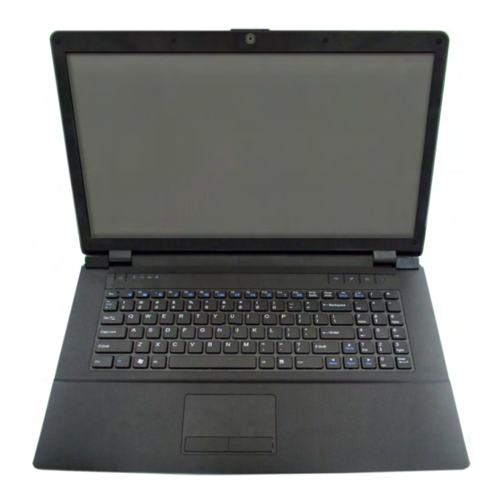
Page 16: External Locator - Top View With Lcd Panel Open
Introduction External Locator - Top View with LCD Panel Open Figure 1 Top View 1. PC Camera (Optional) 2. LCD 3. Power Button 4. GPU Button 5. LED Indicators 6. Hot Key Buttons 7. Keyboard 8. Built-In Microphone 9. Touchpad & Buttons 1 - 4 External Locator - Top View with LCD Panel Open... -
Page 17: External Locator - Front & Right Side Views
Introduction External Locator - Front & Right Side Views Figure 2 Front View 1. LED Indicators Figure 3 Right Side View 1. Headphone-Out Jack 2. Microphone-In Jack 3. S/PDIF-Out Jack 4. USB 2.0 Port 5. Optical Device Drive Bay 6. Emergency Eject Hole External Locator - Front &... -
Page 18: External Locator - Left Side & Rear View
Introduction External Locator - Left Side & Rear View Figure 4 Left Side View 1. External Monitor Port 2. RJ-45 LAN Jack 3. HDMI-Out Port 4. USB 2.0 Port 5. 2 * USB 3.0 Ports 6. Vent 7. eSATA Port 8. -
Page 19: External Locator - Bottom View
Introduction External Locator - Bottom View Figure 5 Bottom View 1. Battery 2. Component Bay Cover 3. Vent 4. Hard Disk Bay Cover 5. Speakers Overheating To prevent your com- puter from overhea- ting, make sure no- thing blocks any vent while the computer is in use. -
Page 20: Mainboard Overview - Top (Key Parts)
Introduction Mainboard Overview - Top (Key Parts) Figure 6 Mainboard Top Key Parts 1. JMC251C 2. KBC-ITE IT8502E 3. Audio Codec 1 - 8 Mainboard Overview - Top (Key Parts) -
Page 21: Mainboard Overview - Bottom (Key Parts)
Introduction Mainboard Overview - Bottom (Key Parts) Figure 7 Mainboard Bottom Key Parts 1. CPU Socket (no CPU installed) 2. Memory Slots DDR3 SO-DIMM 3. Mini-Card Connector (WLAN Module) 4. Platform Controller 5. Multi-in-1 Card Reader Mainboard Overview - Bottom (Key Parts) 1 - 9... -
Page 22: Mainboard Overview - Top (Connectors)
Introduction Mainboard Overview - Top (Connectors) Figure 8 Mainboard Top Connectors 1. HDMI-Out Port 2. USB 2.0 Port 3. USB 3.0 Ports 4. eSATA Port 5. LED Cable Connector 6. Microphone Cable Connector 7. Audio Cable Connector 8. TouchPad Cable Connector 9. -
Page 23: Mainboard Overview - Bottom (Connectors)
Introduction Mainboard Overview - Bottom (Connectors) Figure 9 Mainboard Bottom Connectors 1. Battery Connector 2. CMOS Battery Connector 3. Speaker Cable Connector 4. CPU Fan Cable Connector 5. RJ-45 LAN Jack 6. External Monitor Port 7. DC-In Jack 8. LCD Cable Connector 9. -
Page 24: Disassembly
Chapter 2: Disassembly Overview This chapter provides step-by-step instructions for disassembling the W170HN series notebook’s parts and subsystems. When it comes to reassembly, reverse the procedures (unless otherwise indicated). We suggest you completely review any procedure before you take the computer apart. -
Page 25: Maintenance Tools
Disassembly NOTE: All disassembly procedures assume that the system is turned OFF, and disconnected from any power supply (the battery is removed too). Maintenance Tools The following tools are recommended when working on the notebook PC: • M3 Philips-head screwdriver •... -
Page 26: Maintenance Precautions
Disassembly Maintenance Precautions The following precautions are a reminder. To avoid personal injury or damage to the computer while performing a re- moval and/or replacement job, take the following precautions: Power Safety Warning 1. Don't drop it. Perform your repairs and/or upgrades on a stable surface. If the computer falls, the case and other Before you undertake components could be damaged. -
Page 27: Disassembly Steps
Disassembly Disassembly Steps The following table lists the disassembly steps, and on which page to find the related information. PLEASE PERFORM THE DISASSEMBLY STEPS IN THE ORDER INDICATED. To remove the Battery: 1. Remove the battery page 2 - 5 To remove the HDD: 1. -
Page 28: Removing The Battery
Disassembly Removing the Battery Figure 1 Battery Removal 1. Turn the computer off, and turn it over. 2. Slide the latch in the direction of the arrow (Figure 1a a. Slide the latch and hold it 3. Slide the latch in the direction of the arrow, and hold it in place (Figure 1a in place. -
Page 29: Removing The Hard Disk Drive
Disassembly Removing the Hard Disk Drive The hard disk drive can be taken out to accommodate other 2.5" serial (SATA) hard disk drives with a height of 9.5mm Figure 2 (h). Follow your operating system’s installation instructions, and install all necessary drivers and utilities (as outlined in HDD Assembly Chapter 4 of the User’s Manual) when setting up a new hard disk. - Page 30 Disassembly 3. Remove the hard disk bay cover (Figure 3b Figure 3 4. Grip the tab and slide the hard disk in the direction of arrow (Figure 3c HDD Assembly 5. Lift the hard disk assembly out of the bay (Figure 3d Removal (cont’d.) 6.
-
Page 31: Removing The Optical (Cd/Dvd) Device
Disassembly Removing the Optical (CD/DVD) Device Figure 4 Optical Device 1. Turn off the computer, remove the battery (page 2 - 5) and hard disk (page 2 - Removal 2. Remove the screw at point (Figure 4a 3. Use a screwdriver to carefully push out the optical device at point (Figure 4b a. -
Page 32: Removing The System Memory (Ram)
Disassembly Removing the System Memory (RAM) Figure 5 RAM Module The computer has two memory sockets for 200 pin Small Outline Dual In-line Memory Modules (SO-DIMM) supporting Removal DDRIII (DDR3) Up to 1333/1600MHz. The main memory can be expanded up to 8GB. The SO-DIMM modules sup- ported are 1024MB and 2048MB DDRIII Modules. - Page 33 Disassembly 4. Gently pull the two release latches ( & ) on the sides of the memory socket in the direction indicated by the Figure 6 arrows (Figure 5c). The RAM module will pop-up Figure 6d , and you can then remove it RAM Module 5.
-
Page 34: Removing And Installing A Processor
Disassembly Removing and Installing a Processor Figure 7 Processor Removal Processor Removal Procedure 1. Turn off the computer, remove the battery (page 2 - 5) and the component bay cover (page 2 - a. Remove the cover and 2. The CPU heat sink will be visible at point (Figure 7a) on the mainboard. - Page 35 Disassembly 4. Carefully lift up the heat sink (Figure 8c) off the computer. 5. Turn the release latch towards the unlock symbol , to release the CPU (Figure 8d). Figure 8 6. Carefully (it may be hot) lift the CPU up out of the socket (Figure 8e).
- Page 36 Disassembly Processor Installation Procedure Figure 9 1. Insert the CPU (Figure 9a), pay careful attention to the pin alignment, it will fit only one way (DO NOT FORCE Processor Installation IT!), and turn the release latch towards the lock symbol (Figure 9b).
-
Page 37: Removing The Wireless Lan Module
Disassembly Removing the Wireless LAN Module Figure 10 Wireless LAN 1. Turn off the computer, turn it over, and remove the battery (page 2 - 5) and the component bay cover (page 2 - Module Removal 2. The Wireless LAN module will be visible at point on the mainboard (Figure 10a). -
Page 38: Removing The Keyboard
Disassembly Removing the Keyboard Figure 11 Keyboard Removal 1. Turn off the computer and remove the battery (page 2 - 2. Remove the screws and use a screwdriver to carefully push out the top cover module at point (Figure a. Remove the screws and 11a). - Page 39 Disassembly 2 - 16...
-
Page 40: Part Lists
Appendix A:Part Lists This appendix breaks down the W170HN series notebook’s construction into a series of illustrations. The component part numbers are indicated in the tables opposite the drawings. Note: This section indicates the manufacturer’s part numbers. Your organization may use a different system, so be sure to cross-check any relevant documentation. -
Page 41: Part List Illustration Location
Part List Illustration Location The following table indicates where to find the appropriate part list illustration. Table A - 1 Part List Illustration Part W170HN Location page A - 3 page A - 4 Bottom page A - 5 page A - 6... -
Page 42: Top
Figure A - 1 非耐落 黑色 灰色 Top A - 3... -
Page 43: Bottom
Bottom Figure 2 Bottom A - 4 Bottom... -
Page 44: Lcd
Figure A - 3 LCD A - 5... -
Page 45: Sata Blu-Ray Combo
SATA BLU-RAY Combo Figure A - 4 SATA BLU-RAY Combo (非耐落) A - 6 SATA BLU-RAY Combo... -
Page 46: Sata Dvd
SATA DVD Figure A - 5 SATA DVD (非耐落) SATA DVD A - 7... -
Page 47: Hdd
Figure A - 6 A - 8 HDD... - Page 48 Schematic Diagrams Appendix B: Schematic Diagrams This appendix has circuit diagrams of the W170HN notebook’s PCB’s. The following table indicates where to find the appropriate schematic diagram. Diagram - Page Diagram - Page Diagram - Page Table B - 1...
-
Page 49: Schematic Diagrams
Schematic Diagrams System Block Diagram VDD3,VDD5 W150HNM/W170HN Huron River System Block Diagram W150HNM 7IN1 6-7P- W1507- 001 W150HNM MAIN BOARD GPU NVDIDA N12x NVVDD 6-71- W1500- D02 PCIE*8 AUDIO BOARD PHONE JACK x3, USB x1 5V,3V,5VS,3VS,1.5VS, RJ-11 6-71- W150A- D02 Sandy Bridge 1.8VS,+1.5S_CPU... -
Page 50: Cpu 1/7 (Dmi, Peg, Fdi
Schematic Diagrams CPU 1/7 (DMI, PEG, FDI) Sandy Bridge Processor 1/7 ( DMI,PEG,FDI ) 1 . 0 5V S _ V T T U 4 9 A 20 mil J 2 2 P E G _ I R C OM P _ R R 1 3 3 2 4 . -
Page 51: Cpu 2/7 (Clk, Misc, Jtag
Schematic Diagrams CPU 2/7 (CLK, MISC, JTAG) Sandy Bridge Processor 2/7 ( CLK,MISC,JTAG ) Processor Pullups/Pull downs PU/PD for JTAG signals 1 . 0 5 V S _ V T T 1 . 05 V S _ V T T H _ P R O C H OT # 6 2_ 0 4 R 1 1 0... -
Page 52: Cpu 3/7 (Ddr3
Schematic Diagrams CPU 3/7 (DDR3) Sandy Bridge Processor 3/7 ( DDR3 ) U49C U 49D AB 6 AE 2 M _A _DQ[63:0] S A_C LK[0] M _A_C LK _DDR 0 9 M _B _DQ [ 63 : 0] S B _CLK [ 0 ] M _B _CLK _DDR 2 10 AA 6 AD 2... -
Page 53: Cpu 4/7 (Power
Schematic Diagrams CPU 4/7 (Power) Sa ndy Br idg e Pro ces sor 4/ 7 ( P OWE R ) POWER U4 9F PRO CESSO R CORE POWE R PR OCESSO R UNCO RE PO WER V COR E 4 8A 8.5A 1.05V S _V T T 1.05V S _VT T... -
Page 54: Cpu 5/7 (Graphics Power
Schematic Diagrams CPU 5/7 (Graphics Power) Sandy Bridge Processor 5/7 ( GRAPHICS POWER ) 1 . 5 V 10/2 2 POWER U 4 9 G R 2 6 3 V G F X _ C OR E 10/ 21 Q 18 1K _1 % _ 04 A T 2 4 A K 35... -
Page 55: Cpu 6/7 (Gnd
Schematic Diagrams CPU 6/7 (GND) Sandy Bridge Processor 6/7 ( GND ) U49H U49I AT35 AJ22 V SS1 V SS 8 1 AT32 AJ19 V SS2 V SS 8 2 AT29 AJ16 V SS3 V SS 8 3 VS S161 V SS234 AT27 AJ13... -
Page 56: Cpu 7/7 (Reserved)
Schematic Diagrams CPU 7/7 (RESERVED) Sandy Bridge Processor 7/7 ( RESERVED ) CFG Straps for Processor PEG St atic L ane Re versal - CFG2 is fo r the 16x 1 . 5V CFG2 1:(De fault) Norma l Oper ation; Lane # R 6 4 2 *0 _ 0 4 defin ition matche s sock et pin map de finiti on... -
Page 57: Ddr3 So-Dimm_0
Schematic Diagrams DDR3 SO-DIMM_0 SO-DIMM A CHANGE TO STANDARD C 3 5 4 * 10 p _ 50 V _ N P O _ 04 M _ A _C L K _D D R 0 M_ A _ C L K _ D D R # 0 J D I M M1 A M_ A _ A [ 1 5: 0 ] M _ A _ D Q[ 6 3 : 0 ] 4... -
Page 58: Ddr3 So-Dimm_1
Schematic Diagrams DDR3 SO-DIMM_1 SO-DIMM B CHANGE TO STANDARD J D I M M2 B C 40 5 *1 0 p _5 0 V _ N P O _ 04 M _ B _ C L K _ D D R 2 M _B _C L K _ D D R # 2 1 . -
Page 59: Panel, Inverter, Crt
Schematic Diagrams Panel, Inverter, CRT 3 . 3 V S PANEL POWER PANEL CONNECTOR (LED+EDP) R 28 R 2 7 PL VD D LV DS :3 .3 V 2A J_ L C D 1 eD P 3D :5 V 3A R N 8 0 _ 8P 4 R _0 4 L V D S -U C L K N _C OM B O... -
Page 60: Vga Pci-E Interface
Schematic Diagrams VGA PCI-E Interface G PU H 1 1 H 13 H 8_0D 4_4 H 8 _0D 4_4 H 8_0D 4_4 U 46A P E X _V D D 1/ 1 6 P C I _E X P R E S S A K 1 6 P E X _I O V D D A K 1 7... -
Page 61: Vga Frame Buffer Interface
Schematic Diagrams VGA Frame Buffer Interface Frame Buf fer Interface U 46B U 46C 2/ 1 6 FB A 3/ 1 6 FB B FB C _ D [ 63: 0] FB V D D Q FB C _ D [ 63: 0] FB A _D [ 63: 0] FB V D D Q FB A _D [ 63: 0]... -
Page 62: Vga Frame Buffer A
Schematic Diagrams VGA Frame Buffer A Frame Buffer Partition A F B A _ C MD [ 31 : 0 ] FB A _ C M D [ 31 : 0] F B A _D [ 63: 0] F B A _D [ 63: 0 ] F B V D D Q F B A D Q M[ 7: 0 ] F B V D D Q... -
Page 63: Vga Frame Buffer C
Schematic Diagrams VGA Frame Buffer C F B C _C MD [ 3 1: 0] FB C _C MD [ 3 1: 0] Frame Buffer Partition C F B C _D [ 63 : 0 ] F B C _D [ 63 : 0 ] F B C D Q M[ 7 : 0] F B C D QM[ 7 : 0] F B V D D Q... -
Page 64: Vga I/O
Schematic Diagrams VGA I/O U 46 H U 46 I 8 / 1 6 I F P C 9 /1 6 IF PE F U 46 O U 46 P 1 0 /1 6 MIOA 1 1 /1 6 MIOB A J 9 A A 9 I FP C _P L LV D D... -
Page 65: Vga Nvvdd Cecoupling
Schematic Diagrams VGA NVVDD Cecoupling U 46M 1 5/1 6 GND A A11 G ND A A12 G ND A A13 G ND A A14 G ND A A15 G ND A A16 G ND A A17 G ND A A18 G ND A A19 G ND... -
Page 66: Cougarpoint
Schematic Diagrams CougarPoint - M 1/9 NO R EBO OT S TR AP R TC V C C CougarPoint - M (HDA,JTAG,SATA) NO RE BO OT S TRA P: H DA_ SP KR Hi gh E nab le D 2 8 3 . -
Page 67: Cougarpoint - M 2/9
Schematic Diagrams CougarPoint - M 2/9 CougarPoint - M (PCI-E,SMBUS,CLK) 3 . 3 V 9 /3 U 5 4B R N 6 2 . 2 K _ 8P 4R _ 0 4 B G 34 S MB _ C L K P C I E _ R X N 1 _U S B 3 0 _ V L I P E R N 1 B J 34... -
Page 68: Cougarpoint - M 3/9
Schematic Diagrams CougarPoint - M 3/9 CougarPoint -M (DMI,FDI,GPIO) U 5 4 C B C 2 4 B J 14 D M I _ R X N 0 D M I 0 R X N F D I _ R X N 0 F D I _ T X N 0 B E 2 0 A Y 1 4... -
Page 69: Cougarpoint - M 4/9
Schematic Diagrams CougarPoint - M 4/9 CougarPoint -M (LVDS,DDI) U 5 4 D J 4 7 A P 4 3 B L O N M 4 5 L _B K LT E N S D V O_ T V C L K I N N A P 4 5 1 1 , 3 4 N B _ E N A V D D... - Page 70 Schematic Diagrams CougarPoint - M 5/9 C ouga rPo int -M (PC I,U SB, NVRA M) U54 E A Y7 3.3V RN 7 RS VD 1 A V 7 10K _8P 4R_04 RS VD 2 BG 26 A U3 A C_P RE SE NT T P 1 RS VD 3 B J26...
- Page 71 Schematic Diagrams CougarPoint - M 6/9 3. 3V CougarPoint - M (GPIO,VSS_NCTF,RSVD) R569 1K _04 HOS T_A LE RT#1 R295 1K _04 HO ST_A LE RT#2 3.3V S 10/21 U54 F R401 *10K _04 DGP U_P WR OK R402 1K _04 S A TA_ ODD_P W RGT S_ GPIO C 40...
-
Page 72: Cougarpoint - M 7/9
Schematic Diagrams CougarPoint - M 7/9 CougarPoint -M (POWER) 3 . 3V S L5 2 H C B 16 0 8 K F -1 2 1T 2 5 POWER U 5 4G 1 . 0 5V S V C C A _ D A C _ 3 . 3 V S 5 V S L5 1 H C B 16 0 8 K F -1 2 1T 2 5... -
Page 73: Cougarpoint - M 8/9
Schematic Diagrams CougarPoint - M 8/9 CougarPoint - M (POWER) CougarPoint power supply range 1 . 05 V S _ V C C A _ C L K L 5 0 *H C B 1 0 0 5K F -12 1 T 20 Voltage 1 . -
Page 74: Cougarpoint - M 9/9
Schematic Diagrams CougarPoint - M 9/9 CougarPoint -M (GND) Vo ltag e R ail Vol tage S0 I ccm ax C urr ent (A) V_ CPU_ IO 1. 05 1 (m A) U 54I V5 REF 1 (m A) U54H A Y4 V5 REF_ Sus 1 (m A) -
Page 75: Wlan, 3G, Mini Pcie
Schematic Diagrams WLAN, 3G, Mini PCIE 3G/MSATA MINI CARD 3G POWER FP CONN C 5 75 2 2 0u _ 6 . 3V _ 6 . 3 *6 . 3 *4 . 2 GN D C 5 82 0. 1 u _ 16 V _ Y 5 V _ 0 4 P J 43 W140HN ONLY 1 0 /2 2... -
Page 76: Usb, Fan, Tp, Fp, Multi-Conn
Schematic Diagrams USB, Fan, TP, FP, Multi-Conn USB Charge PORT 10/ 28 V D D 5 U S B V C C 0 1 U S B _P N 0 U S B _ P N 0 _ R C 4 89 R 43 5 0_ 0 4 *1 0u _ 1 0V _ Y 5V _ 0 8... -
Page 77: Usb 3.0
Schematic Diagrams USB 3.0 VL I VL 8012 USB3 .0 3. 3 V_NEC 3. 3 V_NEC 3 . 3VA 1. 0 5V_NEC 3. 3 VA 3.3 V _VI A F or US B 3. 0 L eg a cy R40 4 * 1 0K_04 3 . -
Page 78: Card Reader (Jmc251C
Schematic Diagrams Card Reader (JMC251C) S D _ C L K JMC251 C 3 . 3V _L A N S wit ch in g Re gul at or C 2 65 nea r Pi n#41 c los e to P IN 33 D V D D *1 0p _ 5 0V _N P O_ 0 6 R 1 9 3... -
Page 79: Sata Odd, Led, Hotkey, Lid Sw
Schematic Diagrams SATA ODD, LED, Hotkey, LID SW SATA ODD Zero Power ODD W140XX ONLY 5 V S 3 . 3 V S W140XX ONLY J _ OD D 1 Z e ro_ V I N R 1 79 * 15 m i l _ s ho rt _ 0 6 C7 7 4 *0 . -
Page 80: Hdmi, Rj45
Schematic Diagrams HDMI, RJ45 11/ 5 EM I LAN POART GIGA LAN (JMC251C) *W C M2 0 12 F 2 S -1 6 1T 0 3 -sh o rt L 4 4 L 1 5 J _ R J _ 1 LA N _ MD I P 0 L M X1 + *W C M2 0 12 F 2 S -1 6 1T 0 3 -sh o rt... -
Page 81: Audio Codec Alc269
Schematic Diagrams Audio Codec ALC269 CODEC (ALC269 & VT1802P) P V D D 1 _ 2 R 3 12 La yout not e: * 1 5m i l _ s h o rt _0 6 R 3 5 6 * 0_ 0 4 GND a nd AUDG spa ce i s 1 . -
Page 82: Kbc-Ite It8518E
Schematic Diagrams KBC-ITE IT8518E K B C _ A V D D L 1 9 H C B 1 0 05 K F -1 2 1T 2 0 V D D 3 V D D 3 C 6 85 C 2 9 4 C 68 4 C 3 19 C 34 6... -
Page 83: 5Vs, 3Vs, 3.3Vm, 1.5Vs_Cpu
Schematic Diagrams 5VS, 3VS, 3.3VM, 1.5VS_CPU V D D 3 V I N V D D 3 10/ 28 10/13 U 2 0 R 2 2 1 1 0/22 V I N 1 V I N 1 R 2 6 0 10 K _ 0 4 P R 2 1 7 *1 2 . -
Page 84: Vdd3, Vdd5
Schematic Diagrams VDD3, VDD5 V R E F _ V D D P R 87 * 0 _ 04 P R 88 0 _ 0 4 P C 5 8 1 u_ 1 0 V _ Y 5 V _ 0 6 V F B 2 V F B 1 P R 9 1... -
Page 85: Power 0.85Vs, 1.8Vs, Pex_Vdd
Schematic Diagrams Power 0.85VS, 1.8VS, PEX_VDD PEX_VDD 1.8VS NM OS S Y S 1 5 V 1. 0 5 V S 1.05V@4A P E X_ V D D P Q 5 A 250 MIL M TN N 2 0 N 0 3 Q8 P R 22 2 P J 1 *1 0 m i l _ s ho rt... -
Page 86: Power 1.5V/1.05Vs/0.75V
Schematic Diagrams Power 1.5V/1.05VS/0.75V P D 17 V I N P U 6 P Q 55 P C 1 8 2 P C 9 0 P C 8 9 P C 8 3 ME 48 9 4 -G u P 6 1 63 R B 05 4 0 S 2 V D D Q VTT_MEM... -
Page 87: Power V-Core1
Schematic Diagrams Power V-Core1 1.05VS_VTT P R 21 2 10 _ 04 P C 1 64 6 80 p _ 50 V _ X 7R _0 4 VCORE_1 P R 2 0 9 1 . 2 k_ 1 % _0 4 B~43 50 PUT COLSE 10/13... -
Page 88: Power V-Core2
Schematic Diagrams Power V-Core2 VI N VCORE_2 P C 1 54 P C 1 5 3 P C 1 5 2 +P C 17 7 P R 31 2. 2 _ 0 6 P C 2 7 0 . 22 u _ 10 V _ X 7R _ 06 P Q 4 1 P Q4 0 M D U 26 5 7... -
Page 89: Power Vga Nvvdd
Schematic Diagrams Power VGA NVVDD 1 029 0.975 V 0.825 V 0.8V NVVD D_VID 0 NVVD D_VID 1 VDD3 S ET0 S ET2 S ET1 S ET3 1108 3V 3_RUN PR 138 10K_04 PC101 0.047u_10V _X 7R_04 P S_N VV DD_P GOOD # 37 P R123 P Q20 10K _04... -
Page 90: Ac_In, Charger
Schematic Diagrams AC_IN, Charger P R 5 0 _ 0 4 Charge Current : 3.0A V I N P Q 2 M E P 4 43 5 Q8 C ha rg e V ol ta ge 12 .6 V Total Power : 80W 11/5 EMI J _ D C -J A C K 1 P L 1... -
Page 91: W150Hnm Audio Board
Schematic Diagrams W150HNM Audio Board USB PORT(PORT3) A _ U S B V CC A L 6 A _ U S B V C C 2 H CB 1 6 08 K F -1 2 1 T2 5 60 mil A C 1 9 A C 1 1 A C 3... -
Page 92: W150Hnm Second Hdd Board
Schematic Diagrams W150HNM Second HDD Board OJ _O D D 1 OJ _SA TA 1 O _D S AT A_TXP 2 O_ H S ATA _TXP 1 O_D SA TA _TXP 2 OC 15 0. 01u_16V _X7R _04 OC 16 0. -
Page 93: B5100 Click Board
Schematic Diagrams B5100 Click Board C SW1~ 2 V15XX CLICK BOARD T 3 . 3V T + 5 V S C C 1 RIGHT LIFT T + 5V S 0 . 1 u_ 1 0V _X 7 R _ 0 4 F C R 7 *3 2 mi l _ sh o rt C S W 2... -
Page 94: B5100 Fingerprint Board
Schematic Diagrams B5100 Fingerprint Board V51XX FINGERPRINT BOARD FPJ T1 FP U 1 FR E G_OUT FR EF _OS C FB D R IV E1 FU S B_C ON N FB D R IV E2 FAV D D U SB_C ON N EC T FBE ZE L1 FB D RI V E1 FXI N... -
Page 95: B5100 Led & Vga Sw Board
Schematic Diagrams B5100 LED & VGA SW Board HDD LED BT LED BL_3. 3VS BL_3. 3VS BLJ_LED 1 BL_3.3VS BL_LED _I GP U# BL_LED _D GPU# BL_VGA_SW # BL_BT_EN BLR1 BLR7 BL_SATA_LE D# BLR 2 BL_OPTIMU S_MOD E 220_04 220_04 BL_WLAN_LED# 220_04 BLD1... -
Page 96: B5100 Power Switch Board
Schematic Diagrams B5100 Power Switch Board V51XX POWER SWITCH BOARD BH_3. 3V S BVD D 3 BH _3.3VS BJ_SW1 BR 1 BVD D3 BVDD 3 BVD D 3 BVDD 3 680_06 BPW R BTN # P OWER BW EB#0 BD 4 BD 1 BD 3 B UTTON... -
Page 97: Sequence
Schematic Diagrams Sequence P B 5 0 / P B 7 0 H u r o n R i v e r P O W E R S E Q U E N C E VCCRTC 36mS RTCRST # SPEC DD_ON# 1. -
Page 98: Updating The Flash Rom Bios
Download the BIOS computer model. 1. Go to www.clevo.com.tw and point to E-Services and click E-Channel. Note that BIOS versions 2. Use your user ID and password to access the appropriate download area (BIOS), and download the latest BIOS files... -
Page 99: Use The Flash Tools To Update The Bios
BIOS Update Use the flash tools to update the BIOS 1. Make sure you are not loading any memory management programs such as HIMEM by holding the F8 key as you see the message “Starting MS-DOS”. You will then be prompted to give “Y” or “N” responses to the programs being loaded by DOS. - Page 100 www.s-manuals.com...
Need help?
Do you have a question about the W170HN and is the answer not in the manual?
Questions and answers