Table of Contents
Advertisement
Quick Links
Si5365/66/67/68/69 E
1. Introduction
The Si5365/66-EVB,Si5367/68-EVB, and Si5369-EVB provide platforms for evaluating Silicon Laboratories'
Si5365/Si5366, Si5367/Si5368, and Si5369 Any-Frequency Precision Clocks. The Si5365 and Si5366 are
controlled directly using configuration pins on the devices, while the Si5367, Si5368, and Si5369 are controlled by
a microprocessor or MCU (microcontroller unit) via an I
clock multipliers with a loop bandwidth ranging from 30 kHz to 1.3 MHz. The Si5366 and Si5368 are jitter-
attenuating clock multipliers, with a loop bandwidth ranging from 60 Hz to 8.4 kHz. The Si5369 is similar to the
Si5368, with a much lower loop BW of from 4 to 525 Hz. The Si5366 device can optionally be configured to operate
as a Si5365, so a single evaluation board is available to evaluate both devices. Likewise, the Si5368 can be
configured to operate as a Si5367, so the two devices share a single evaluation board.
The Si5365/66/67/68/69 Any-Frequency Precision Clocks are based on Silicon Laboratories' 3rd-generation
®
DSPLL
technology, which provides any-frequency synthesis in a highly integrated PLL solution that eliminates the
need for external VCXO and loop filter components. The devices have excellent phase noise and jitter
performance. The Si5366, Si5368, and Si5369 jitter attenuating clock multipliers support jitter generation of 0.3 ps
RMS (typ) across the 12 kHz–20 MHz and 50 kHz–80 MHz jitter filter bandwidths. The Si5365 and SI5367 support
jitter generation of 0.6 ps RMS (typ) across the 12 kHz–20 MHz and 50 kHz–80 MHz jitter filter bandwidths. For all
devices, the DSPLL loop bandwidth is digitally programmable, providing jitter performance optimization at the
application level. These devices are ideal for providing clock multiplication/clock division, jitter attenuation, and
clock distribution in mid-range and high performance timing applications.
Rev. 0.6 1/12
VALUATION
Top
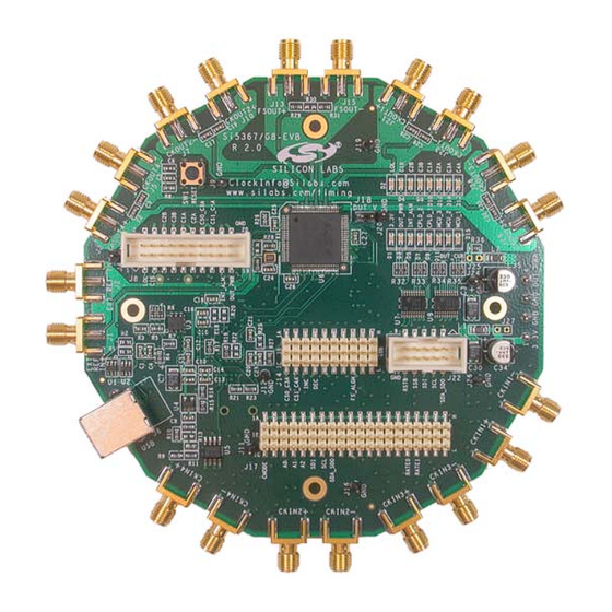
Figure 1. Si536x TQFP EVB
Copyright © 2012 by Silicon Laboratories
Si5365/66-EVB
Si5367/68-EVB
B
OA RD
2
C or SPI interface. The Si5365 and Si5367 are low jitter
Bottom
Si5369-EVB
U
'
G
SER
S
U ID E
Si536x-EVB
Advertisement
Table of Contents

Related Manuals for Silicon Laboratories Si5365-EVB


Summary of Contents for Silicon Laboratories Si5365-EVB
- Page 1 Si5365, so a single evaluation board is available to evaluate both devices. Likewise, the Si5368 can be configured to operate as a Si5367, so the two devices share a single evaluation board. The Si5365/66/67/68/69 Any-Frequency Precision Clocks are based on Silicon Laboratories' 3rd-generation ®...
- Page 2 (LVPECL, LVDS, CML, CMOS), output phase adjustment between output clocks, and output phase adjustment between all output clocks and the selected reference input clock (phase increment/decrement). For more details, consult the Silicon Laboratories timing products website at www.silabs.com/timing.
- Page 3 5. Connect a USB cable from the EVB to the PC where the software was installed. 6. Install USB driver. 7. Launch software by clicking on Start Programs Silicon Laboratories Precision Clock EVB Software and selecting one of the programs. Rev. 0.6...
-
Page 4: Functional Description
Si5365/66-EVB Si5367/68-EVB Si5369-EVB 5. Functional Description The Si5365/66-EVB, Si5367/68-EVB, Si5369-EVB, and DSPLLsim software allow for a complete and simple evaluation of the functions, features, and performance of the Si536x Any-Frequency Precision Clocks. 5.1. Narrowband versus Wideband Operation This document describes three evaluation boards: one for the Si5365 and Si5366, another for the Si5367 and Si5368, and a third for the Si5369. - Page 5 Si5365/66-EVB Si5367/68-EVB Si5369-EVB 5.3. Si536x Input and Output Clocks The Si536x has four differential inputs that are ac terminated to 50 and then ac coupled to the part. Single ended operation can be implemented by simply not connecting to one of the two of the differential pairs. When operating with clock inputs of 1 MHz or less in frequency, the appropriate dc blocking capacitors (C58, C61, C47, C50, C53, C55, C42 and C45) located on the bottom of the board should be replaced with zero ohm resistors.
- Page 6 Si5365/66-EVB Si5367/68-EVB Si5369-EVB 5.4. CPLD This CPLD is required for the MCU to control an Si536x operating at either 1.8, 2.5, or 3.3 V. The CPLD provides two main functions: it translates the voltage level from 3.3 V (the MCU voltage) to the Si536x voltage (either 1.8, 2.5, or 3.3 V).
- Page 7 Si5365/66-EVB Si5367/68-EVB Si5369-EVB 5.6. Power and 2L Signals This evaluation board requires two power inputs +3.3 V for the MCU and either 1.8, 2.5, or 3.3 V for the Any- Frequency Precision Clock part. The power connector is J40. The grounds for the two supplies are tied together on the EVB.
-
Page 8: Connectors And Leds
Si5365/66-EVB Si5367/68-EVB Si5369-EVB 6. Connectors and LEDs 6.1. LEDs There are sixteen LEDs on the board which provide a quick and convenient means of determining board status. Table 3. LED Status and Description Color Label Color Label green 3.3 V green DUT_PWR ALRMOUT... - Page 9 Si5365/66-EVB Si5367/68-EVB Si5369-EVB 6.2. User Jumpers and Headers. Use Figure 4 to locate the jumpers described in Tables 4, 5, 6, and 7: Ext Ref, J1, J2 Ext Ref, J1, J2 R24, R28, C22 on top; R24, R28, C22 on top; R50, R51, R52, C39 on bot R50, R51, R52, C39 on bot J25, R36...
- Page 10 Si5365/66-EVB Si5367/68-EVB Si5369-EVB J14 is a three-pin by ten header that is used to establish input levels for the pin controlled two-level inputs using jumper plugs. It also provides a means of externally driving the two-level input signals: Table 4. Two-Level Input Jumper Header, J14 Comment J14.1B CS0_C3A...
- Page 11 Si5365/66-EVB Si5367/68-EVB Si5369-EVB Table 6. External Serial Port Connector, J22 Comment J22.1 SDA_SDO J22.3 SCL_SCLK J22.5 J22.7 A2_SS J22.9 DUT_RST_B reset J17 is a three-pin by twenty header that is used to establish input levels for the pin controlled three-level inputs using jumper plugs.
-
Page 12: Evb Software Installation
Si5365/66-EVB Si5367/68-EVB Si5369-EVB 7. EVB Software Installation The release notes and the procedure for installing the EVB software can be found on the release CD included with the EVB. These items can also be downloaded from the Silabs web site: www.silabs.com/timing. Follow the links for 1-PLL Jitter attenuators, and look under the Tools tab. - Page 13 Si5365/66-EVB Si5367/68-EVB Si5369-EVB 8. Schematics Figure 5. Si536x Rev. 0.6...
- Page 14 Si5365/66-EVB Si5367/68-EVB Si5369-EVB Rev. 0.6...
- Page 15 Si5365/66-EVB Si5367/68-EVB Si5369-EVB Rev. 0.6...
- Page 16 Si5365/66-EVB Si5367/68-EVB Si5369-EVB Rev. 0.6...
- Page 17 Si5365/66-EVB Si5367/68-EVB Si5369-EVB Rev. 0.6...
-
Page 18: Bill Of Materials
Si5365/66-EVB Si5367/68-EVB Si5369-EVB 9. Bill of Materials Table 9. Si536x Bill of Materials Item Qty Reference Part Mfgr MfgrPartNum C1,C2,C3,C5,C10,C12,C17,C19,C21 100 N Venkel C0603X7R160-104KNE ,C25,C26,C27,C28,C29,C32,C33,C3 6,C37,C38,C40,C42,C44,C45,C47,C 49,C50,C53,C55,C57,C58,C60,C61 C4,C6,C8,C9,C14,C23,C52 1 UF Venkel C0603X7R6R3- 105KNE C7,C30,C31 33 UF Venkel TA0006TCM336MBR C11,C13,C15,C16,C18,C20,C24,C41 10 NF Venkel C0603X7R160-103KNE ,C43,C46,C48,C51,C54,C56,C59,C6... - Page 19 Si5365/66-EVB Si5367/68-EVB Si5369-EVB Table 9. Si536x Bill of Materials (Continued) Item Qty Reference Part Mfgr MfgrPartNum R15,R19,R28,R29,R31,R36,R38, 0 ohm Venkel CR0603-16W-000T R48,R73 66.5 Venkel CR0603-16W-66R5FT R27,R58 Venkel CR0603-16W-1000FT R32,R33,R34,R35 R150x4 Panasonic EXB-38V151JV Venkel CR0603-16W-1130FT 82.5 Venkel CR0603-16W-82R5FT Mountain Switch 101-0161-EV U1,U2 SN65220 SN65220DBVT...
- Page 20 Si5365/66-EVB Si5367/68-EVB Si5369-EVB 10. Layout Figure 10. Silkscreen Top Figure 11. Layer 1 Rev. 0.6...
- Page 21 Si5365/66-EVB Si5367/68-EVB Si5369-EVB Figure 12. Layer 2, Ground Plane Figure 13. Layer 3 Rev. 0.6...
- Page 22 Si5365/66-EVB Si5367/68-EVB Si5369-EVB Figure 14. Layer 4, 3.3 V Power Figure 15. Layer 5 Rev. 0.6...
- Page 23 Si5365/66-EVB Si5367/68-EVB Si5369-EVB Figure 16. Layer 6, DUT Power Figure 17. Layer 7, Ground Plane Rev. 0.6...
- Page 24 Si5365/66-EVB Si5367/68-EVB Si5369-EVB Figure 18. Layer 8 Figure 19. Silkscreen Bottom Rev. 0.6...
-
Page 25: Default Settings
Si5365/66-EVB Si5367/68-EVB Si5369-EVB —P PPENDIX OWERUP AND ACTORY EFAULT ETTINGS For the Si5367/68-EVB and the Si5369-EVB, the power up settings are as follows: 19.44 MHz input on either CKIN1, CKIN3 or CKIN4 CKIN2 is not used because of free run mode 155.52 MHz output on CKOUT1 and CKOUT2 622.08 MHz output on CKOUT3 and CKOUT4 311.04 MHz output on CKOUT5... - Page 26 Si5365/66-EVB Si5367/68-EVB Si5369-EVB For J14: Jumper Comment CS0_C3A J14.1B none CS1_C4A J14.2B none J14.3B none J14.4B none — J14.5B none — J14.6B none DBL34 J14.7B none CKOUT3, CKOUT 4 enabled FS_ALIGN J14.8B none no FS alignment FS_SW J14.9B none CKIN3, CKIN 4 not LOS inputs CK_CONF J14.10B none...
-
Page 27: Document Change List
Si5365/66-EVB Si5367/68-EVB Si5369-EVB OCUMENT HANGE Revision 0.2 to Revision 0.3 Updated "5.3.Si536x Input and Output Clocks" on page 5. Updated "5.5.MCU" on page 6. Added "Appendix—Powerup and Factory Default Settings" on page 25. Revision 0.3 to Revision 0.4 ... - Page 28 Si5365/66-EVB Si5367/68-EVB Si5369-EVB OTES Rev. 0.6...
- Page 29 The products must not be used within any Life Support System without the specific written consent of Silicon Laboratories. A "Life Support System" is any product or system intended to support or sustain life and/or health, which, if it fails, can be reasonably expected to result in significant personal injury or death.
Need help?
Do you have a question about the Si5365-EVB and is the answer not in the manual?
Questions and answers