Icom IC-FR3000 Service Manual
Vhf fm repeater
Hide thumbs
Also See for IC-FR3000:
- Sales handbook (74 pages) ,
- Instruction manual (24 pages) ,
- Remote control manual (14 pages)
Table of Contents
Advertisement
Advertisement
Chapters
Table of Contents

Related Manuals for Icom IC-FR3000


Summary of Contents for Icom IC-FR3000
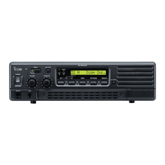
- Page 1 VHF FM REPEATER iC-fr3000 iC-fr3 1 0 0...
- Page 2 DO NOT short any circuits or electronic parts. An insu- lated tuning tool MUST be used for all adjustments. <SAMPLE ORDER> DO NOT keep power ON for a long time when the re- 1110003780 S.IC NJM2902V IC-FR3000 LOGIC UNIT 1 piece peater is defective. 8930056450 2368 6-key IC-FR3000 CHASSIS...
-
Page 3: Table Of Contents
TABLE OF CONTENTS SECTION 1 SPECIFICATIONS SECTION 2 INSIDE VIEWS SECTION 3 CIRCUIT DESCRIPTION 3 - 1 RECEIVER CIRCUITS ....................3 - 1 3 - 2 TRANSMITTER CIRCUITS .................... 3 - 3 3 - 3 PLL CIRCUITS......................... 3 - 4 3 - 4 OTHER CIRCUITS ...................... - Page 4 SECTION 1 SPECIFICATIONS [USA2], [GEN2], [GEN4] [EUR2], [FRG2] Measurement method EIA / TIA-603 ETS 300 086 Frequency range 150.000–174.000 MHz W/N (25 kHz; Wide / 12.5 kHz; Narrow): 16K0F3E / 8K50F3E Type of emission [USA2], [GEN2], [GEN4], [EUR2] M/N (20 kHz; Middle / 12.5 kHz; Narrow): 14K0F3E / 8K50F3E [FRG2] 25 or 12.5 kHz (Wide / Narrow) Channel spacing...
- Page 5 SECTION 2 INSIDE VIEWS • BOARD LAYOUT *: Located under side of this point. JACK2 unit* JACK1 unit* REG unit PA unit TX unit RX unit LOGIC unit* FRONT unit • PA UNIT Top view Power amplifier (IC2: S-AV32 50 W type S-AV33 25 W type) APC CTRL (IC1: TA75S01F...
- Page 6 • LOGIC UNIT Top view Ringer detect circuit (IC48: TLP121) DTMF decoder (IC30: TC4W53FU, IC31: LC7387M) CTCSS decoder (IC29: FX805LG) EEPROM (IC37: HN58X2464TI) (IC33: HD64F2238BF) Splatter filter (IC4: NJM2902V) D/A converter (IC25: M62364) Temperature switching Mic mix amplifier circuit (IC32: TC4W53) (IC2: NJM2902V) AF amplifier (IC17: LA4425A)
- Page 7 • TX UNIT Top view *: Located under side of this point. TX VCO circuit Mixer (IC6: NJM2107F) D/A converter* (IC5: M62364FP) PLL reference oscillator 12.8 MHz (X1: CR-759) PLL IC* (IC2: MB1511PFV) • RX UNIT Top view *: Located under side of this point. PLL IC* RF amplifier (IC4: MB1511PFV)
-
Page 8: Circuit Description
SECTION 3 CIRCUIT DESCRIPTION 3-1 RECEIVER CIRCUITS suppressed and are then applied to a limiter amplifier sec- tion in the system IC (IC2, pin 5). 3-1-1 RF CIRCUIT (RX UNIT) Received signals from the RX antenna connector enter the IC2 contains the 2nd mixer, limiter amplifier, quadrature RX unit J1 and pass through a tuned bandpass filter (D3, detector, active filter and noise amplifier circuits, etc. -
Page 9: Transmitter Circuits
3-1-6 RECEIVER MUTE CIRCUITS (LOGIC UNIT) The DTCS signal passes through a low-pass filter circuit (IC12, pins 1, 3, 8, 10), and is then applied to the DTCS • NOISE SQUELCH decoder which is inside the CPU (IC33, pin 52) via the The noise squelch circuit cuts out AF signals when no RF “DTCSI”... - Page 10 The mixed signals are applied to the splatter filter (IC4). 3-2-3 POWER AMPLIFIER CIRCUIT (PA UNIT) The power amplifier circuit amplifies the driver signal to an • INCASE OF THE AF SIGNALS FROM THE ANTENNA output power level. CONNECTOR The AF signals (received signals) from the antenna connec- The RF signal from the TX unit is applied to the pre-drive tor (RX unit;...
-
Page 11: Pll Circuits
3-3 PLL CIRCUITS 3-3-5 TRANSMITTER PLL CIRCUIT (TX UNIT) The PLL IC (IC2) which includes in the prescaler, the pro- 3-3-1 GENERAL grammable counter and the phase comparator. The PLL IC Each receiver and transmitter circuit has an independent sets the divided ratio which bases on N-data from the CPU PLL circuit for controlling frequencies. -
Page 12: Other Circuits
3-5 POWER SUPPLY CIRCUITS 3-4 OTHER CIRCUIT 3-5-1 LOGIC AND REG UNITS VOLTAGE LINES 3-4-1 TELEPHONE IF CIRCUIT (LOGIC UNIT) The signals from the telephone line (FRONT, J13) are Line Description applied to the ringer detect circuit (IC48, D1, D5, R131, R143, R145, C100, C103, C375). -
Page 13: Port Allocations
3-6 PORT ALLOCATIONS 3-6-3 EXPANDER IC (LOGIC UNIT; IC41) 3-6-1 EXPANDER IC (LOGIC UNIT; IC39) Port Port Description Description number name number name Outputs the control signal for “BASE” Outputs the switch control signal for BASL LED on the FRONT unit. R/BSW the received AF signal to the micro- phone amplifier. - Page 14 3-6-6 CPU (LOGIC UNIT; IC33) 3-6-5 D/A CONVERTER IC (TX UNIT; IC5) Port Port Description Description number name number name Outputs the strobe signal for the PLL Input port for the TONE signal from RPLSTB ETONE IC (RX unit; IC4). the ACC connector.
- Page 15 CPU-Continued CPU-Continued Port Port Description Description number name number name Outputs the strobe signal for the port Input port for the RV SWR signal from PE3STB RVSWR expander IC (LOGIC unit; IC41). the PA unit. Input port for the temperature signals Outputs the strobe signal for the port PE2STB TEMP...
-
Page 16: Adjustment Procedures
SECTION 4 ADJUSTMENT PROCEDURES 4-1 PREPARATION Some adjustments must be performed on the “ADJUSTMENT MODE”. Refer to the next page in detail. I REQUIRED TEST EQUIPMENT EQUIPMENT GRADE AND RANGE EQUIPMENT GRADE AND RANGE Output voltage : 13.6 V DC Frequency range : 300–3000 Hz DC power supply... - Page 17 I ENTERING THE ADJUSTMENT MODE 1 Turn the power OFF. 2 Push and hold [CH-DN] and [CH-UP] buttons, then turn the power ON, keep on pushing [CH-DN] and [CH-UP] buttons until sounds 1 beep audio. 3 Push [CH-DN] button, then sounds 2 beep audio. I EXITING THE ADJUSTMENT MODE 1 Turn the power OFF.
- Page 18 ADJUSTMENT MODE CH LIST LCD DISPLAY ADJUSTMENT 173.925 173.725 A01 LW TXREF *** TVCO/RVCO adjustment. Reference frequency adjustment. 173.925 173.725 RX sensitivity adjustment. A02 LW HRTUN *** 162.075 162.275 RX sensitivity adjustment. A03 LW MRTUN *** 150.075 150.275 RX sensitivity adjustment. A04 LW LRTUN *** 150.075 150.275...
-
Page 19: Pll Adjustmenst
4-2 PLL ADJUSTMENT MEASUREMENT ADJUSTMENT ADJUSTMENT ADJUSTMENT CONDITIONS VALUE UNIT LOCATION UNIT ADJUST TX VCO LOCK • LCD display : A01 LW TXREF 127 Connect a digital multi 4.0 V TVCO VOLTAGE • Transmitting meter or oscilloscope to check point CP4. RX VCO LOCK •... - Page 20 • IC-FR3000 TOP VIEW PA UNIT TX UNIT DC/REG UNITS RX UNIT • RX UNIT TOP VIEW • TX UNIT TOP VIEW Reference frequency check point CP18 TX VCO lock voltage check point C17 (RVCO unit) C17 (TVCO unit) RX VCO lock voltage...
-
Page 21: Receiver Adjustment
4-3 RECEIVER ADJUSTMENT MEASUREMENT ADJUSTMENT ADJUSTMENT ADJUSTMENT CONDITIONS VALUE UNIT LOCATION UNIT ADJUST • LCD display : A02 LW HRTUN Connect a digital multi Maximum FRONT [PRT/BASE] SENSITIVITY • Connect a standard signal generator meter or oscilloscope voltage /[MONI] to the [RX] antenna connector and set to check point CP18. -
Page 22: Software Adjustment
4-4 SOFTWARE ADJUSTMENT Select an operation using [CH-UP] / [CH-DN] keys, then set specified value using [RPT/BASE] / [MONI] keys on the FRONT PANEL. MEASUREMENT ADJUSTMENT ADJUSTMENT CONDITION VALUE UNIT LOCATION OUTPUT • LCD display : A06 HW POWER Rear Connect an RF power meter to 50.0 W POWER... - Page 23 SOFTWARE ADJUSTMENT – continued Select an operation using [CH-UP] / [CH-DN] keys, then set specified value using [RPT/BASE] / [MONI] keys on the FRONT PANEL. MEASUREMENT ADJUSTMENT ADJUSTMENT CONDITION VALUE UNIT LOCATION DTCS • LCD display : A11 LW DTCADJ Rear Connect an FM deviation meter Set to flat wave...
-
Page 24: Parts List
SECTION 5 PARTS LIST [REG UNIT] [REG UNIT] ORDER ORDER DESCRIPTION DESCRIPTION 1180001320 NJM7809FA 4030006900 S.CERAMIC C1608 JB 1H 103K-T 1180002290 S.IC NJM7809DL1A-TE 4030006860 S.CERAMIC C1608 JB 1H 102K-T 1180001860 S.IC TA78M05F (TE16L) 4510007660 ELECTROLYTIC LXZ25VB100 1180002480 S.REG TA78DL12AF (TE16L) 4510007660 ELECTROLYTIC LXZ25VB100... -
Page 25: Front Unit
[FRONT UNIT] [FRONT UNIT] ORDER ORDER DESCRIPTION DESCRIPTION 1530002060 S.TRANSISTOR 2SC4081 T106 R 6910014540 SPACER LM-10 6910014540 SPACER LM-10 6910014540 SPACER LM-10 1750000930 S.DIODE NNCD8.2C-T1 6910014540 SPACER LM-10 1750000930 S.DIODE NNCD8.2C-T1 1750000930 S.DIODE NNCD8.2C-T1 6200001620 S.COIL ELJFC 1R0K-F [LOGIC UNIT] ERJ3GEYJ 471 V (470 Ω) 7030003400 S.RESISTOR... - Page 26 [LOGIC UNIT] [LOGIC UNIT] ORDER ORDER DESCRIPTION DESCRIPTION 1160000150 S.TRANSISTOR IMZ4 T108 7030003600 S.RESISTOR ERJ3GEYJ 223 V (22 kΩ) 1590001960 S.TRANSISTOR XP4311 (TX) 7030003680 S.RESISTOR ERJ3GEYJ 104 V (100 kΩ) 1590001960 S.TRANSISTOR XP4311 (TX) 7030003680 S.RESISTOR ERJ3GEYJ 104 V (100 kΩ) 1540000570 S.TRANSISTOR 2SD1760 TLQ...
- Page 27 [LOGIC UNIT] [LOGIC UNIT] ORDER ORDER DESCRIPTION DESCRIPTION R144 7030000480 S.RESISTOR MCR10EZHJ 6.8 kΩ R243 7030003680 S.RESISTOR ERJ3GEYJ 104 V (100 kΩ) R145 7030000410 S.RESISTOR MCR10EZHJ 1.8 kΩ R245 7030003570 S.RESISTOR ERJ3GEYJ 123 V (12 kΩ) R148 7030003760 S.RESISTOR ERJ3GEYJ 474 V (470 kΩ) R246 7410001140 S.ARRAY...
- Page 28 [LOGIC UNIT] [LOGIC UNIT] ORDER ORDER DESCRIPTION DESCRIPTION R371 7030003640 S.RESISTOR ERJ3GEYJ 473 V (47 kΩ) R521 7030003640 S.RESISTOR ERJ3GEYJ 473 V (47 kΩ) ERJ3GEYJ 100 V (10 Ω) R372 7030003200 S.RESISTOR R522 7030003520 S.RESISTOR ERJ3GEYJ 472 V (4.7 kΩ) MCR100JZHJ 10 Ω...
- Page 29 [LOGIC UNIT] [LOGIC UNIT] ORDER ORDER DESCRIPTION DESCRIPTION 4030017490 S.CERAMIC C1608 JB 1A 105K-T C184 4030007090 S.CERAMIC C1608 CH 1H 470J-T 4030011600 S.CERAMIC C1608 JB 1E 104K-T C185 4030007090 S.CERAMIC C1608 CH 1H 470J-T 4030011600 S.CERAMIC C1608 JB 1E 104K-T C186 4030007090 S.CERAMIC...
- Page 30 [LOGIC UNIT] [LOGIC UNIT] ORDER ORDER DESCRIPTION DESCRIPTION C292 4550006250 S.TANTALUM TEESVA 1A 106M8L C441 4030018060 S.CERAMIC C5750 JB 2E 474KT C294 4550006250 S.TANTALUM TEESVA 1A 106M8L C442 4030017490 S.CERAMIC C1608 JB 1A 105K-T C295 4550006250 S.TANTALUM TEESVA 1A 106M8L C443 4030006900 S.CERAMIC...
- Page 31 [RX UNIT] [RX UNIT] ORDER ORDER DESCRIPTION DESCRIPTION ERJ3GEYJ 181 V (180 Ω) 1190000450 S.IC GN2011-Q (TX) 7030003350 S.RESISTOR 1110003490 S.IC TA31136FN (D,EL) [EUR2], [FRG2] 1180000420 S.IC TA78L05F (TE12R) 7030003670 S.RESISTOR ERJ3GEYJ 823 V (82 kΩ) 1140002130 S.IC MB1511PFV-G-BND [USA2], [GEN2], [GEN4] 1110002750 S.IC TA75S01F (TE85R)
- Page 32 [RX UNIT] [RX UNIT] ORDER ORDER DESCRIPTION DESCRIPTION R155 7030003520 S.RESISTOR ERJ3GEYJ 472 V (4.7 kΩ) 4030006960 S.CERAMIC C1608 CH 1H 050C-T R156 7030003620 S.RESISTOR ERJ3GEYJ 333 V (33 kΩ) 4030006860 S.CERAMIC C1608 JB 1H 102K-T R157 7030003680 S.RESISTOR ERJ3GEYJ 104 V (100 kΩ) 4510004630 S.ELECTROLYTIC ECEV1CA100SR...
- Page 33 [RX UNIT] [RVCO UNIT] ORDER ORDER DESCRIPTION DESCRIPTION C198 4030008880 S.CERAMIC C1608 JB 1H 223K-T 1560000490 S.FET 2SK508 K52 T2B C199 4030006860 S.CERAMIC C1608 JB 1H 102K-T 1530002920 S.TRANSISTOR 2SC4226-T1 R25 C200 4030006860 S.CERAMIC C1608 JB 1H 102K-T C201 4550006250 S.TANTALUM TEESVA 1A 106M8L C202...
- Page 34 [TX UNIT] [TX UNIT] ORDER ORDER DESCRIPTION DESCRIPTION 1180000420 S.IC TA78L05F (TE12R) 7030003530 S.RESISTOR ERJ3GEYJ 562 V (5.6 kΩ) 1140002130 S.IC MB1511PFV-G-BND 7030003520 S.RESISTOR ERJ3GEYJ 472 V (4.7 kΩ) 1110002400 S.IC NJM2107F-TE1 7030003480 S.RESISTOR ERJ3GEYJ 222 V (2.2 kΩ) 1180000430 S.IC TA78L06F (TE12L) 7030003600...
- Page 35 [TX UNIT] [TVCO UNIT] ORDER ORDER DESCRIPTION DESCRIPTION 4030006860 S.CERAMIC C1608 JB 1H 102K-T 1560000490 S.FET 2SK508 K52 T2B 4030006860 S.CERAMIC C1608 JB 1H 102K-T 1530003260 S.TRANSISTOR 2SC5006-T1 4030006860 S.CERAMIC C1608 JB 1H 102K-T 4030006860 S.CERAMIC C1608 JB 1H 102K-T 4030006860 S.CERAMIC C1608 JB 1H 102K-T...
- Page 36 [PA UNIT] [PA UNIT] ORDER ORDER DESCRIPTION DESCRIPTION 1110002750 S.IC TA75S01F (TE85R) 7030003440 S.RESISTOR ERJ3GEYJ 102 V (1 kΩ) 1150002110 S-AV33 (I) [EUR2], [FRG2] [EUR2], [FRG2] 1150002160 S-AV32 (I2) 7030003460 S.RESISTOR ERJ3GEYJ 152 V (1.5 kΩ) [USA2], [GEN2], [GEN4] [USA2], [GEN2], [GEN4] 1110002400 S.IC NJM2107F-TE1...
-
Page 37: Vr Unit
[PA UNIT] [JACK1 UNIT] ORDER ORDER DESCRIPTION DESCRIPTION C112 4030011600 S.CERAMIC C1608 JB 1E 104K-T 6200009940 S.COIL BLM21PG221SN1 [USA2], [GEN2], [GEN4] 6200009940 S.COIL BLM21PG221SN1 6200009940 S.COIL BLM21PG221SN1 6200009940 S.COIL BLM21PG221SN1 6510022800 S.CONNECTOR B10B-PH-SM3-TB 6200009940 S.COIL BLM21PG221SN1 6510007020 CONNECTOR TMP-J01X-V6 6200009940 S.COIL BLM21PG221SN1 6200009940... - Page 38 [JACK2 UNIT] [CHASSIS UNIT] ORDER ORDER DESCRIPTION DESCRIPTION 1750000930 S.DIODE NNCD8.2C-T1 6510022970 CONNECTOR N-PA-JJ (NI) 1750000930 S.DIODE NNCD8.2C-T1 1750000930 S.DIODE NNCD8.2C-T1 1750000930 S.DIODE NNCD8.2C-T1 2510001200 SPEAKER C057FA510-10 1750000930 S.DIODE NNCD8.2C-T1 1750000930 S.DIODE NNCD8.2C-T1 1750000930 S.DIODE NNCD8.2C-T1 2710000750 FBA08A12LZ 1750000930 S.DIODE NNCD8.2C-T1 2710000740 FBA06A12L...
- Page 39 SECTION 6 OPTION UNIT INSTALLATION I Opening the repeater’s case Follow the case and cover opening procedures shown here when an optional unit is installed or adjust the in- ternal units, etc. CAUTION: DISCONNECT the AC power cable and/or DC power cable from the repeater. Other- wise, there is danger of electric shock and/or equip- ment damage.
- Page 40 SECTION 7 MECHANICAL PARTS AND DISASSEMBLY [CHASSIS PARTS] [LOGIC UNIT] ORDER ORDER QTY. QTY. DESCRIPTION DESCRIPTION 8900011521 OPC-1049A (Power SW cable) 6910014900 FRC-50-12-6.5 8900011571 OPC-1055A (LOGIC-JACK2 cable A) 6910014890 FRC-WC1 8900011580 OPC-1056 (LOGIC-JACK2 cable B) 8900011590 OPC-1057 (LOGIC-JACK1 cable) 5210000030 Fuse FGB 1A (FGB0 125V) 8900011681 OPC-1183A (LOGIC-VR cable)
- Page 41 MP17 MP84 FRONT UNIT MP84 EP3 (L) MP82 EP2 (F) W5 (L) MP69 MP84 JACK1 UNIT MP82 EP2 (L) W4 (L) MP68 EP3 (F) MP82 MP84 MP16 EP4 (F) EP7 (F) MP84 MP86 MP68 EP6 (F) MP82 MP27 EP5 (F) MP10 MP68 MP84...
- Page 42 MP64 MP64 MP100 MP18 NOTE (R): REG UNIT MP64 MP64 (RX): RX UNIT MP100 (TX): TX UNIT MP64 (PA): PA UNIT MP64 (RVCO): RVCO UNIT MP54 MP55 (TVCO): TVCO UNIT MP54 MP55 Parts without designation are CHASSIS PARTS. MP64 MP74 MP64 MP53 MP74...
-
Page 43: Tvco Unit
[CHASSIS PARTS] [RX UNIT] ORDER ORDER QTY. QTY. DESCRIPTION DESCRIPTION 8510015120 2368 A-case 6510022970 Connector N-PA-JJ(NI) 8510015130 2368 B-case 8510015140 2368 E-case 8900011510 OPC-1048 (AC input cable) 8900011531 OPC-1050A (Back up DC cable) 8510015480 2367 shield case 8900011540 OPC-1052 (PS output cable) 8900011550 OPC-1053 (REG-LOGIC cable) 8900011560... - Page 44 SECTION 8 SEMI-CONDUCTOR INFORMATION 8 - 1 TRANSISTORS AND FETS 2SC3661-TB 2SA1362-Y 2SA1576A T106R 2SB1182 TL Q 2SC2712-BL (Symbol: AEY) (Symbol: FR) (Symbol: B1182, (Symbol: LL) (Symbol: FY) 2SC4081 T106 R 2SC4226-T1 R25 2SC4703-T2 SF 2SC4116-Y 2SC4215-O (Symbol: BR) (Symbol: R25) (Symbol: SF) (Symbol: LY) (Symbol: QO)
- Page 45 8 - 2 DIODES 1SS226 (TE85R) 1SS268 (TE85R) 1SS319 (TE85R) 1SS355 TE-17 1SV305 (TPL3) (Symbol: C3) (Symbol: BF) (Symbol: A4) (Symbol: A) (Symbol: TV) HSU88TRF 1SV308 (TPL3) D1UBA80-4062 DSA3A1 FCH30A03L (Symbol: TX) (Symbol: UA80) (Symbol: None) (Symbol: FCH30A03L) (Symbol: 9) Green A, C A, C...
- Page 46 The combination of this page and the next page shows SECTION 9 BOARD LAYOUTS the unit layout in the same configuration as the actual P.C. Board. 9 - 1 FRONT UNIT ¡ TOP VIEW to LCD DS7 9 - 2 VR UNIT 9 - 3 TVCO UNIT 9 - 4 RVCO UNIT ¡TOP VIEW...
- Page 47 FRONT UNIT The combination of this page and the previous page shows the unit layout in the same configuration as the ¡BOTTOM VIEW to LOGIC UNIT J4 actual P.C. Board. to LOGIC UNIT J3 to LOGIC UNIT – to JACK1 UNIT J3 RVCO UNIT TVCO UNIT...
- Page 48 9 - 5 LOGIC UNIT The combination of this page and the next page shows the unit layout in the same configuration as the actual ¡TOP VIEW P.C. Board. to JACK1 UNIT J3 to JACK2 UNIT J2 to JACK2 UNIT J3 3 4 5 6 7 8 9 10 11 12 13 SQLVRI SQLVRO...
- Page 49 to OPTIONAL UNIT LOGIC UNIT The combination of this page and the previous page shows the unit layout in the same configuration as the ¡BOTTOM VIEW actual P.C. Board. MICO SDTO MICI RPLSTB to RX UNIT J2 RUNLK W/NS RSSI to OPTIONAL RVCON SIGOUT...
- Page 50 9 - 6 RX UNIT The combination of this page and the next page shows the unit layout in the same configuration as the actual ¡TOP VIEW P.C. Board. RX ANT RX OUT to LOGIC UNIT J1 9 - 5...
- Page 51 RX UNIT The combination of this page and the previous page shows the unit layout in the same configuration as the ¡BOTTOM VIEW actual P.C. Board. 9 - 6...
- Page 52 9 - 7 TX UNIT The combination of this page and the next page shows to PA UNIT the unit layout in the same configuration as the actual ¡ TOP VIEW P.C. Board. to LOGIC UNIT J2 FWSWR RVSWR PATEMP TMUTE2 ETONE I TONE...
- Page 53 TX UNIT The combination of this page and the previous page shows the unit layout in the same configuration as the ¡BOTTOM VIEW actual P.C. Board. 9 - 8...
- Page 54 9 - 8 PA UNIT ¡ TOP VIEW TX ANT TXRFIN to REG UNIT to REG UNIT The combination of this page and the next page shows the unit layout in the same configuration as the actual to TX UNIT J4 P.C.
- Page 55 PA UNIT ¡BOTTOM VIEW TXRFIN to REG UNIT to REG UNIT The combination of this page and the previous page shows the unit layout in the same configuration as the actual P.C. Board. to TX UNIT J1 9 - 10...
- Page 56 AC IN 9 - 9 REG UNIT POWER The combination of this page and the next to LOGIC UNIT J6 PS 0V page shows the unit layout in the same BATTERY ¡TOP VIEW DC SUPPLY PS 15V configuration as the actual P.C. Board. to LOGIC to PA FAN to REG FAN...
- Page 57 REG UNIT The combination of this page and the previous page shows the unit layout in the same configuration as the ¡BOTTOM VIEW actual P.C. Board. BATTERY to PA UNIT BATTERY to PA UNIT PS 15V PS 15V PS 0V PS 0V –...
- Page 58 SECTION 10 BLOCK DIAGRAM SCK,SDTO,DA1STB,TPLSTB IC13: BU4066BCFV TUNLK IC1: NJM2902V IC4D IC4: NJM2902V Q1: XP1214 IC1D MIC MUTE PATEMP from FRONT UNIT SW-D CTDTO FWSWR TONE IC2: NJM2902V IC3: NJM2902V from CPU RVSWR IC4A, B, C UNIT IC2D IC2C IC2A, B IC3A IC3B VCC2...
- Page 59 IC7: TA78L05F IC1: TA78L05F D15: MA29W B D4: MA2S111 IC4: TA78L06F TVCO UNIT Q6: 2SC3661 PATEMP RIPLE D1: 1SV305 FILTER IC3: NJM2107F D2: 1SV305 D3: 1SV305 IC5: M62364FP IC2: S-AV32 (50W type) D1: 1SV308 D2: HSU88 D4: 1SV305 S-AV33 (25W type) Q2: 2SC4226 D5: 1SV305 D4: HSU88...
- Page 60 SECTION 11 WIRING DIAGRAM DISPLAY W4 (LOGIC) REMOTE RX UNIT SPMUTE MICE CLONE W10 (LOGIC) <W18 (CHASSIS), W19 (CHASSIS)> M PTT to SP MIC RVCO MICE CLONE UNIT M PTT M MONI M MONI SDTO RPLSTB RX OUT W17 (CHASSIS) RUNLK W/NS TELG...
- Page 61 SECTION 12 VOLTAGE DIAGRAM REMOTE REMOTE SP MUTE FREE: 4.7V SPMUTE PUSH: 0.0V S7 SKQDPB S8 SKQDPB MICE 5.0V 3.8V to LOGIC UNIT J4 CLONE M PTT M MONI REMOTE SP MUTE RPT/BASE MONI MSC-C161UYLY-4W FREE: 4.2V PUSH: 0.0V S6 SKQDPB S5 SKQDPB Q1 2SC4081 to JACK1 UNIT J3...
- Page 62 [USA2, GEN2, GEN4] R184 12 CP20 R186 [EUR2], [FRG2] 22nH 12[EUR2], [FRG2] 470p 22[USA2], [GEN2], R197 [USA2], [GEN2], 47nH 0.001 3.3k 100p [GEN4] [GEN4] 39nH 47nH 0.001 458DB-1011 0.001 0.39µH [EUR2], 2.9V 0.01 0.001 RX RFIN [FRG2] RX ANT GN2011-Q R183 C223 458DB-1011...
- Page 63 8.3V 2.2µH 3.4V 1µH 0.001 0.001 2SC4215 0.001 0.001 36CS-656LZ-09K=P3 1SV308 1SV308 0.001 22nH 1SV305 to PA UNIT 4.9V 1µH 1.7V C121 0.001 0.001 0.001 0.001 2.2nH 2SK508 2.1V TX OUT 3.3V UNTX: 9.1V 2.2µH 2.2µH 1.7V LQW2BHNR10J01L 3.9k 2SC5006 TX OUT 1SV305 1SV305...
- Page 64 13.6V S-AV33 (I) BL01RN1A1D2B LA-563A LA-536A [EUR2], [FRG2] VCC1 S-AV32 (I2) REG UNIT [USA2], [GEN2], [GEN4] Beads CD-CL030H-6R0 REG UNIT 1.2k 0.001 0.01 0.001 0.01 0.001 0.01 470p 0.001 0.01 [EUR2], [FRG2] [EUR2], [FRG2] 1.5k 1.5k [USA2], [GEN2], [GEN4] [USA2], [GEN2], [GEN4] C106 C105 C107...
- Page 65 C366 R453 10 LIMIT C383 22p S MIX IC4A IC4C IC2A IC3A SPLATTER FILTER MIC MIX PRE-EMP IC2C IC2B NJM2902V NJM2902V IC13 C380 R497 2.5V NJM2902V NJM2902V R23 330k IC3B R118 5.0V NJM2902V NJM2902V BU4066BCFV 4.7k 100k 2.0V NJM2902V C364 C408 1.9V C382...
- Page 66 Mount B-Side to FRONT UNIT J2 to FRONT UNIT J1 to RX UNIT J2 to TX UNIT J3 1 2 3 4 5 6 7 8 9 10 11 12 13 14 15 16 17 18 19 20 21 22 1 2 3 4 5 6 7 8 9 10 11 12 13 14 15 16 17 18 19 20 21 22 13.6V L4 BLM31PG121SN1...
- Page 67 AC IN CHASSIS UNIT POWER PS 0V PS 0V DC SUPPLY PS 15V M SW AC POWER SUPPLY: 15.4V PS 0V DC POWER SUPPLY: 0.0V EP10 PS 15V PS 15V PS 15V M SW PS 0V ATC-20 8.0V FCH30A03L TA78L08F PS 0V PS 15V 2SJ533...
- Page 69 S-14004MZ-C1 1-1-32, Kamiminami, Hirano-ku, Osaka 547-0003, Japan © 2003 Icom Inc.
- Page 70 UHF FM REPEATER iC-fr4000...
- Page 71 INTRODUCTION DANGER This service manual describes the latest service informa- ONLY the specified AC voltage described on the tion for the IC-FR4000 UHF FM REPEATER. AC power socket. Other voltages may causes repeater damage or personal injuy. To upgrade quality, all electrical or mechanical parts and internal circuits are subject to change without notice or DO NOT expose the repeater to rain, snow or any liquids.
- Page 72 TABLE OF CONTENTS SECTION 1 SPECIFICATIONS SECTION 2 INSIDE VIEWS SECTION 3 CIRCUIT DESCRIPTION 3 - 1 RECEIVER CIRCUITS ....................3 - 1 3 - 2 TRANSMITTER CIRCUITS .................... 3 - 3 3 - 3 PLL CIRCUITS......................... 3 - 4 3 - 4 THE OTHER CIRCUITS ....................
- Page 73 SECTION 1 SPECIFICATIONS ‘ ‘ GENERAL • Frequency range : 450–480 MHz • Type of emission : 16K0F3E / 8K50F3E • Frequency resolution : 25 or 12.5 kHz • Number of channels : Max. 32 channel :N-type × 2 (50 Ω) •...
-
Page 74: Logic Unit
SECTION 2 INSIDE VIEWS • BOARD LAYOUT *: Located under side of this point. JACK2 unit* JACK1 unit* REG unit 50PA unit TX unit RX unit LOGIC unit* FRONT unit • 50PA UNIT Top view Power amplifier (Q2: 2SC3102) Pre-drive (IC1: SC-1323) Temp sensor (IC4: NJM2107F... - Page 75 • LOGIC UNIT Top view Ringer detect circuit (IC33: HD64F2238F) OFF-HOOK CTRL (IC47: LC73701M, DTMF decoder IC50: TC4W53) (IC30: TC4W53, IC31: LC738M) CTCSS decoder (IC29: FX805) EEPROM (IC39: BU4094) (IC33: HD64F2238F) Splatter filter (IC4: NJM2902V) D/A converter (IC25: M62364) Temperature switching Mic mix amplifier (IC32: TC4W53) (IC2: NJM2902V)
- Page 76 • TX UNIT Top view *: Located under side of this point. TX VCO circuit Mixer (IC6: NJM2107F) D/A converter* (IC5: M62364FP) PLL reference oscillator 12.8 MHz (X1: CR-732) PLL IC* (IC2: MB15A02PFV1) • RX UNIT Top view *: Located under side of this point. PLL IC* RF amplifier (IC4: MB15A02PFV1)
-
Page 77: Circuit Description
SECTION 3 CIRCUIT DESCRIPTION 3-1 RECEIVER CIRCUITS suppressed, and are then applied to a limiter amplifier sec- tion in the system IC (IC2, pin 5). 3-1-1 RF CIRCUIT (RX UNIT) Received signals from the RX antenna connector enter the IC2 contains the 2nd mixer, limiter amplifier, quadrature RX unit J1 and pass through a tuned bandpass filter ( D3, detector, active filter and noise amplifier circuits, etc. -
Page 78: Transmitter Circuits
3-1-6 RECEIVER MUTE CIRCUITS (LOGIC UNIT) The DTCS signal passes through the low-pass filter circuit (IC12), and is then applied to the DTCS decoder which is • NOISE SQUELCH inside the CPU (IC33, pin 52) via the “DTCSI” line. The noise squelch circuit cuts out AF signals when no RF signals are received. - Page 79 • IN CASE OF THE AF SIGNAL FROM THE ANTENNA 3-2-3 DRIVE AMPLIFIER CIRCUIT (PA UNIT) CONNECTOR The drive amplifier circuit amplifies the VCO oscillating sig- The AF signals (received signals) from the antenna connec- nal to the level needed at the power amplifier. tor (RX unit;...
-
Page 80: Pll Circuits
rent of the drive amplifier (IC1, pin 2) to reduce the output amplifier (Q14) as RX PLL lock voltage. power. 3-3-5 TRANSMITTER PLL CIRCUIT (TX UNIT) The PLL IC (IC2) which includes in the prescaler, the pro- 3-3 PLL CIRCUITS grammable counter and the phase comparator. -
Page 81: Power Supply Circuits
3-5 POWER SUPPLY CIRCUITS 3-4 OTHER CIRCUIT 3-5-1 LOGIC AND REG UNITS VOLTAGE LINES 3-4-1 TELEPHONE IF CIRCUIT (LOGIC UNIT) The signals from the telephone line (FRONT, J13) are Line Description applied to the ringer detect circuit (C100, C103, C375, R131, D1, D5, R143, R145, IC48). -
Page 82: Port Allocations
3-6 PORT ALLOCATIONS 3-6-3 EXPANDER IC (LOGIC UNIT; IC41) 3-6-1 EXPANDER IC (LOGIC UNIT; IC39) Port Port Description Description number name number name Outputs the control signal for “BASE” Outputs the switch control signal for BASL LED on the FRONT unit. R/BSW the received AF signal to the micro- phone amplifier. - Page 83 3-6-5 D/A CONVERTER IC (TX UNIT; IC5) 3-6-6 CPU (LOGIC UNIT; IC33) Port Port Description Description number name number name Input port for the TONE signal from Outputs the strobe signal for the PLL ETONE RPLSTB the ACC connector. IC on the RX unit. Outputs the adjusted external TONE Outputs the strobe signal for the PLL ETONEO...
- Page 84 CPU-Continued CPU-Continued Port Port Description Description number name number name Input port for the RV SWR signal from Outputs the strobe signal for the port RVSWR PE3STB the PA unit. expander IC (LOGIC unit; IC41). Input port for the temperature signals Outputs the strobe signal for the port TEMP PE2STB...
-
Page 85: Adjustment Procedures
SECTION 4 ADJUSTMENT PROCEDURES 4-1 PREPARATION When adjusting the contents on page 4-7, a JIG CABLE is required. Some adjustments must be performed on the “ADJUSTMENT MODE”. Refer to the next page in detail. I REQUIRED TEST EQUIPMENT EQUIPMENT GRADE AND RANGE EQUIPMENT GRADE AND RANGE Output voltage... - Page 86 I ENTERING THE ADJUSTMENT MODE 1 Turn the power OFF. 2 Push and hold [CH-DN] and [CH-UP] buttons, then turn the power ON, keep on pushing [CH-DN] and [CH-UP] buttons until sounds 1 beep audio. 3 Push [CH-DN] button, then sounds 2 beep audio. I EXITING THE ADJUSTMENT MODE 1 Turn the power OFF.
- Page 87 ADJUSTMENT MODE CH LIST LCD DISPLAY BAND ADJUSTMENT 479.275 450.275 A01 LW TXREF *** TVCO/RVCO adjustment. Reference frequency adjustment. 465.075 465.275 RX sensitivity adjustment. A03 LW MRTUN *** 450.075 450.275 RPT SQL adjustment. A05 LW RPTSQL*** 450.075 450.275 TX power adjustment. A06 HW POWER *** 465.075 465.275...
- Page 88 4-2 PLL ADJUSTMENT MEASUREMENT ADJUSTMENT ADJUSTMENT ADJUSTMENT CONDITIONS VALUE UNIT LOCATION UNIT ADJUST TX VCO LOCK • LCD display : A01 LW TXREF Connect a digital multi 1.0 V TVCO VOLTAGE • Receiving meter or oscilloscope to check point CP1. RX VCO LOCK •...
- Page 89 • IC-FR4000 TOP VIEW TX UNIT RX UNIT • RX UNIT TOP VIEW • TX UNIT TOP VIEW CP18 RX VCO lock voltage RX VCO lock voltage chack point adjustment TX VCO lock voltage check point Reference frequency check point TX VCO lock voltage adjustment 4 - 5...
- Page 90 4-3 RX ADJUSTMENT MEASUREMENT ADJUSTMENT ADJUSTMENT ADJUSTMENT CONDITIONS VALUE UNIT LOCATION UNIT ADJUST • LCD display : A03 LW MRTUN Connect a digital multi Maximum SENSITIVITY • Connect a standard signal generator meter or oscilloscope voltage to the RX antenna connector and set to check point CP18.
-
Page 91: Software Adjustment
4-4 SOFTWARE ADJUSTMENT Select an operation using [CH-UP] / [CH-DN] keys, then set specified value using [RPT/BASE] / [MONI] keys on the FRONT PANEL. MEASUREMENT ADJUSTMENT ADJUSTMENT CONDITION VALUE UNIT LOCATION OUTPUT • LCD display : A06 HW POWER Rear Connect an RF power meter to 50.0 W POWER... -
Page 92: Parts List
SECTION 5 PARTS LIST [REG UNIT] [REG UNIT] ORDER ORDER DESCRIPTION DESCRIPTION 1180001320 IC NJM7809FA 4030006860 S.CERAMIC C1608 JB 1H 102K-T 1180002290 S.IC NJM7809DL1A-TE 4510007660 ELECTROLYTIC LXZ25VB100 1180001860 S.IC TA78M05F (TE16L) 4030006860 S.CERAMIC C1608 JB 1H 102K-T 1180002480 S.REG TA78DL12AF (TE16L) 4510007650 S.ELECTROLYTIC EEVHB1C470P 1180001540 S.IC TA78L08F (TE12R) -
Page 93: Front Unit
[FRONT UNIT] [FRONT UNIT] ORDER ORDER DESCRIPTION DESCRIPTION 1530002060 S.TRANSISTOR 2SC4081 T106 R 6910014540 SPACER LM-10 1750000930 S.DIODE NNCD8.2C-T1 1750000930 S.DIODE NNCD8.2C-T1 1750000930 S.DIODE NNCD8.2C-T1 [LOGIC UNIT] 6200001620 S.COIL ELJFC 1R0K-F ORDER DESCRIPTION ERJ3GEYJ 471 V (470 Ω) 7030003400 S.RESISTOR 1110003780 S.IC NJM2902V-TE1 ERJ3GEYJ 100 V (10 Ω) - Page 94 [LOGIC UNIT] [LOGIC UNIT] ORDER ORDER DESCRIPTION DESCRIPTION ERJ3GEYJ 681 V (680 Ω) 1590002430 S.TRANSISTOR DTA144EE TL 7030003420 S.RESISTOR 1510000590 S.TRANSISTOR 2SA1362-Y (TE85L) 7030003510 S.RESISTOR ERJ3GEYJ 392 V (3.9 kΩ) 1160000150 S.TRANSISTOR IMZ4 T108 7030003480 S.RESISTOR ERJ3GEYJ 222 V (2.2 kΩ) ERJ3GEYJ 271 V (270 Ω) 1590001960 S.TRANSISTOR XP4311 (TX)
- Page 95 [LOGIC UNIT] [LOGIC UNIT] ORDER ORDER DESCRIPTION DESCRIPTION R128 7030003680 S.RESISTOR ERJ3GEYJ 104 V (100 kΩ) R230 7030003640 S.RESISTOR ERJ3GEYJ 473 V (47 kΩ) MCR100JZHJ 10 Ω (100) R129 7030006480 S.RESISTOR R231 7030003640 S.RESISTOR ERJ3GEYJ 473 V (47 kΩ) R130 7030003620 S.RESISTOR ERJ3GEYJ 333 V (33 kΩ) R232...
- Page 96 [LOGIC UNIT] [LOGIC UNIT] ORDER ORDER DESCRIPTION DESCRIPTION R341 7030003510 S.RESISTOR ERJ3GEYJ 392 V (3.9 kΩ) R493 7030003480 S.RESISTOR ERJ3GEYJ 222 V (2.2 kΩ) R342 7030003510 S.RESISTOR ERJ3GEYJ 392 V (3.9 kΩ) R494 7030003640 S.RESISTOR ERJ3GEYJ 473 V (47 kΩ) R345 7030003500 S.RESISTOR ERJ3GEYJ 332 V (3.3 kΩ)
- Page 97 [LOGIC UNIT] [LOGIC UNIT] ORDER ORDER DESCRIPTION DESCRIPTION 4030006860 S.CERAMIC C1608 JB 1H 102K-T C161 4030007090 S.CERAMIC C1608 CH 1H 470J-T 4030008850 S.CERAMIC C1608 JB 1H 123K-T C162 4030007090 S.CERAMIC C1608 CH 1H 470J-T 4030010760 S.CERAMIC C1608 CH 1H 331J-T C163 4030007090 S.CERAMIC C1608 CH 1H 470J-T...
- Page 98 [LOGIC UNIT] [LOGIC UNIT] ORDER ORDER DESCRIPTION DESCRIPTION C250 4030011600 S.CERAMIC C1608 JB 1E 104K-T C407 4030011600 S.CERAMIC C1608 JB 1E 104K-T C251 4030011600 S.CERAMIC C1608 JB 1E 104K-T C408 4030007090 S.CERAMIC C1608 CH 1H 470J-T C252 4030011600 S.CERAMIC C1608 JB 1E 104K-T C409 4030006870 S.CERAMIC C1608 JB 1H 222K-T...
- Page 99 [LOGIC UNIT] [RX UNIT] ORDER ORDER DESCRIPTION DESCRIPTION 8900009230 CABLE OPC-908 (P=1 N=10 L=60) 1190000450 S.IC GN2011-Q (TX) 8900008740 CABLE OPC-867 (P=1 N=24 L=60) 1110003490 S.IC TA31136FN (D,EL) 7030003860 S.JUMPER ERJ3GE JPW V 1180000420 S.IC TA78L05F (TE12R) 7030007150 S.JUMPER MCR50JZHJ JPW 1140005990 S.IC MB15A02PFV1-G-BND-ER 8900009270 CABLE...
- Page 100 [RX UNIT] [RX UNIT] ORDER ORDER DESCRIPTION DESCRIPTION 7030003670 S.RESISTOR ERJ3GEYJ 823 V (82 kΩ) R155 7030003520 S.RESISTOR ERJ3GEYJ 472 V (4.7 kΩ) 7030003680 S.RESISTOR ERJ3GEYJ 104 V (100 kΩ) R156 7030003620 S.RESISTOR ERJ3GEYJ 333 V (33 kΩ) 7030003680 S.RESISTOR ERJ3GEYJ 104 V (100 kΩ) R157 7030003680 S.RESISTOR...
- Page 101 [RX UNIT] [RX UNIT] ORDER ORDER DESCRIPTION DESCRIPTION 4030006860 S.CERAMIC C1608 JB 1H 102K-T C199 4030006860 S.CERAMIC C1608 JB 1H 102K-T 4030006860 S.CERAMIC C1608 JB 1H 102K-T C200 4030006860 S.CERAMIC C1608 JB 1H 102K-T 4510004630 S.ELECTROLYTIC ECEV1CA100SR C201 4550006250 S.TANTALUM TEMSVA 1A 106M-8L 4550000460 S.TANTALUM TESVA 1C 105M1-8L...
-
Page 102: Rvco Unit
[RVCO UNIT] [TX UNIT] ORDER ORDER DESCRIPTION DESCRIPTION 1560001280 S.FET 2SK508 K53 T1B 1180000420 S.IC TA78L05F (TE12R) 1530002920 S.TRANSISTOR 2SC4226-T1 R25 1140005990 S.IC MB15A02PFV1-G-BND-ER 1110002400 S.IC NJM2107F-TE1 1180000430 S.IC TA78L06F (TE12L) 1720000640 S.VARICAP 1SV284 (TPH3) 1190001350 S.IC M62364FP 600D 1720000640 S.VARICAP 1SV284 (TPH3) 1110002400 S.IC NJM2107F-TE1... - Page 103 [TX UNIT] [TX UNIT] ORDER ORDER DESCRIPTION DESCRIPTION 7030003520 S.RESISTOR ERJ3GEYJ 472 V (4.7 kΩ) 4550006250 S.TANTALUM TEMSVA 1A 106M-8L 7030003480 S.RESISTOR ERJ3GEYJ 222 V (2.2 kΩ) 4030006860 S.CERAMIC C1608 JB 1H 102K-T 7030003520 S.RESISTOR ERJ3GEYJ 472 V (4.7 kΩ) 4510004630 S.ELECTROLYTIC ECEV1CA100SR 7030003480 S.RESISTOR ERJ3GEYJ 222 V (2.2 kΩ)
- Page 104 [TVCO UNIT] [50PA UNIT] ORDER ORDER DESCRIPTION DESCRIPTION 1530000371 S.TRANSISTOR 2SC3356-T1B R25 1150001680 IC S-AU27AM (ICOM) / SC-1323 1530002920 S.TRANSISTOR 2SC4226-T1 R25 1110002750 S.IC TA75S01F (TE85R) 1180001250 S.IC TA7808F (TE16L) 1110002400 S.IC NJM2107F-TE1 1720000640 S.VARICAP 1SV284 (TPH3) 1180000420 S.IC TA78L05F (TE12R) 1720000640 S.VARICAP...
- Page 105 [50PA UNIT] [50PA UNIT] ORDER ORDER DESCRIPTION DESCRIPTION 7030003560 S.RESISTOR ERJ3GEYJ 103 V (10 kΩ) 4030018430 S.CERAMIC ERF22X 6C2H 6R0D D01L MCR10EZHJ 22 Ω (220) 7030000180 S.RESISTOR 4030009500 S.CERAMIC C1608 CH 1H 0R5B-T ERJ3GEYJ 101 V (100 Ω) 7030003320 S.RESISTOR 4030009530 S.CERAMIC C1608 CH 1H 030B-T 7030003560 S.RESISTOR...
- Page 106 [VR UNIT] [JACK2 UNIT] ORDER ORDER DESCRIPTION DESCRIPTION 7210003110 VARIABLE RK0971110 10KA 1750000930 S.DIODE NNCD8.2C-T1 7210003120 VARIABLE RK0971110 10KB 1750000930 S.DIODE NNCD8.2C-T1 1750000930 S.DIODE NNCD8.2C-T1 1750000930 S.DIODE NNCD8.2C-T1 6510018950 S.CONNECTOR B7B-PH-SM3-TB 1750000930 S.DIODE NNCD8.2C-T1 1750000930 S.DIODE NNCD8.2C-T1 1750000930 S.DIODE NNCD8.2C-T1 0910056093 PCB B 5653C 1750000930 S.DIODE...
- Page 107 [CHASSIS UNIT] ORDER DESCRIPTION 6510022970 CONNECTOR N-PA-JJ (NI) 2510001200 SPEAKER C057FA510-10 2710000750 FAN FBA08A12LZ 2710000740 FAN FBA06A12L 8900011510 CABLE OPC-1048 (AC INPUT CABLE) 8900011520 CABLE OPC-1049 (POWER SW CABLE) 8900011530 CABLE OPC-1050 (BACKUP DC CABLE) 8900011540 CABLE OPC-1052 (PS OUTPUT CABLE) 8900011550 CABLE OPC-1053 (REG-LOGIC CABLE) 8900011560 CABLE...
- Page 108 SECTION 6 OPTION UNIT INSTALLATION I Opening the repeater’s case Follow the case and cover opening procedures shown here when an optional unit is installed or adjust the in- ternal units, etc. CAUTION: DISCONNECT the AC power cable and/or DC power cable from the repeater. Other- wise, there is danger of electric shock and/or equip- ment damage.
- Page 109 SECTION 7 MECHANICAL PARTS AND DISASSEMBLY [CHASSIS PARTS] [LOGIC UNIT] ORDER ORDER QTY. QTY. DESCRIPTION DESCRIPTION 8900011520 OPC-1049 (Power SW cable) 5210000030 Fuse FGB 1A (FGB0 125V) 8900011570 OPC-1055 (LOGIC-JACK2 cable A) 5220000020 Fuse holder S-N5051 8900011580 OPC-1056 (LOGIC-JACK2 cable B) 5220000020 Fuse holder S-N5051 8900011590...
- Page 110 MP17 MP84 FRONT UNIT MP84 MP82 W5 (L) EP2 (F) MP69 MP84 JACK1 UNIT MP82 W4 (L) MP84 MP68 EP3 (F) MP82 MP16 EP4 (F) EP7 (F) MP84 MP86 MP68 EP6 (F) MP82 MP27 EP5 (F) MP10 MP68 MP84 MP86 W3 (L) MP85 MP68...
- Page 111 MP64 MP64 MP100 MP18 MP64 MP64 MP100 MP64 NOTE MP64 (R): REG UNIT MP54 MP55 (RX): RX UNIT MP54 MP55 (TX): TX UNIT (PA): 50PA UNIT MP64 MP74 (RVCO): RVCO UNIT MP64 MP53 (TVCO): TVCO UNIT MP74 MP53 to EP7 (R) to EP2 (PA) MP74 to EP8 (R)
- Page 112 [CHASSIS PARTS] [RX UNIT] ORDER ORDER QTY. DESCRIPTION QTY. DESCRIPTION 8510015120 2368 A-case 6510022970 Connector N-PA-JJ(NI) 8510015130 2368 B-case 8510015140 2368 E-case 8900011510 OPC-1048 (AC input cable) 8930059680 Sponge (HD) 8900011520 OPC-1049 (Power SW cable) 8930059680 Sponge (HD) 8900011530 OPC-1050 (Back up DC cable) 8900011540 OPC-1052 (PS output cable) 8900011550...
- Page 113 SECTION 8 SEMI-CONDUCTOR INFORMATION 8 - 1 TRANSISTORS AND FETS 8 - 2 DIODES 2SA1362-Y 2SA1576A T106R 2SB1143 T 2SB1182 TL Q 2SC2712-BL/GR 1SR154-400 TE25 1SS226 (TE85R) 1SS268 (TE85R) 1SS319 (TE85R) 1SS355 TE-17 (Symbol: AEY) (Symbol: FR) (Symbol: B1143 (Symbol: B1182, Q) (Symbol: BL/LG) (Symbol: 14) (Symbol: C3)
- Page 114 The combination of this page and the next page shows SECTION 9 BOARD LAYOUTS the unit layout in the same configuration as the actual P.C. Board. 9 - 1 FRONT UNIT ¡ TOP VIEW to LCD DS7 2 4 6 8 9 - 2 VR UNIT 9 - 3 TVCO UNIT 9 - 4 RVCO UNIT...
- Page 115 FRONT UNIT The combination of this page and the previous page shows the unit layout in the same configuration as the ¡ ¡ BOTTOM VIEW to LOGIC UNIT J4 actual P.C. Board. to LOGIC UNIT J3 to LOGIC UNIT – to JACK1 UNIT J3 RVCO UNIT...
- Page 116 9 - 5 LOGIC UNIT The combination of this page and the next page shows the unit layout in the same configuration as the actual ¡ ¡ TOP VIEW P.C. Board. to JACK1 UNIT J3 to JACK2 UNIT J2 to JACK2 UNIT J3 3 4 5 6 7 8 9 10 11 12 13 SQLVRI SQLVRO...
-
Page 117: Logic Unit
to OPTIONAL UNIT LOGIC UNIT The combination of this page and the previous page shows the unit layout in the same configuration as the ¡ ¡ BOTTOM VIEW actual P.C. Board. MICO SDTO MICI RPLSTB to RX UNIT J2 RUNLK W/NS RSSI to OPTIONAL... - Page 118 9 - 6 RX UNIT The combination of this page and the next page shows the unit layout in the same configuration as the actual ¡ ¡ TOP VIEW RX ANT P.C. Board. RX OUT to LOGIC UNIT J1 9 - 5...
- Page 119 RX UNIT The combination of this page and the previous page shows the unit layout in the same configuration as the ¡ ¡ BOTTOM VIEW actual P.C. Board. RX OUT 9 - 6...
- Page 120 9 - 7 TX UNIT The combination of this page and the next page shows to 50PA UNIT the unit layout in the same configuration as the actual ¡ ¡ TOP VIEW P.C. Board. to LOGIC UNIT J2 FWSWR RVSWR PATEMP TMUTE2 ETONE...
- Page 121 TX UNIT The combination of this page and the previous page shows the unit layout in the same configuration as the ¡ ¡ BOTTOM VIEW actual P.C. Board. 9 - 8...
- Page 122 9 - 8 50PA UNIT The combination of this page and the next page shows the unit layout in the same configuration as the actual ¡ ¡ TOP VIEW P.C. Board. C125 C126 1 2 3 TX ANT 8 - 9 VARISTER UNIT ¡TOP VIEW to REG UNIT to REG UNIT...
-
Page 123: 50Pa Unit
50PA UNIT The combination of this page and the previous page shows the unit layout in the same configuration as the ¡ ¡ BOTTOM VIEW actual P.C. Board. VARISTER UNIT ¡BOTTOM VIEW) 9 - 10... - Page 124 AC IN 9 - 10 REG UNIT POWER The combination of this page and the next to LOGIC UNIT J6 PS 0V page shows the unit layout in the same BATTERY ¡ ¡ TOP VIEW DC SUPPLY PS 15V configuration as the actual P.C. Board. to LOGIC to PA FAN to REG FAN...
-
Page 125: Reg Unit
REG UNIT The combination of this page and the previous page shows the unit layout in the same configuration as the ¡BOTTOM VIEW actual P.C. Board. BATTERY BATTERY to 50PA to 50PA PS 15V PS 0V PS 0V UNIT EP2 PS 15V –... - Page 126 SECTION 10 BLOCK DIAGRAM SCK,SDTO,DA1STB,TPLSTB IC13: BU4066BCFV TUNLK IC1: NJM2902V IC4D IC4: NJM2902V MIC MUTE Q1: XP1214 IC1D PATEMP from FRONT UNIT SW-D CTDTO FWSWR TONE IC2: NJM2902V IC3: NJM2902V from CPU RVSWR IC4A, B, C IC2D IC2C IC2A, B IC3A IC3B UNIT...
- Page 127 IC5: TA78L05F IC1: TA78L05F VARISTOR UNIT D1: MA29W B D4: MA2S111 IC4: TA78L06F TVCO UNIT Q6: 2SC3661 PATEMP RIPLE D1: 1SV284 FILTER D2: HSU88 IC4: NJM2107F D2: 1SV284 D4: HSU88 D3: 1SV284 IC5: M62364FP D5: MA8047M D4: 1SV284 Q2: 2SC4226 D5: 1SV284 D6: MA8047M Q2: 2SC3102...
-
Page 128: Jack1 Unit
SECTION 11 VOLTAGE DIAGRAM REMOTE REMOTE SP MUTE FREE: 4.7V SPMUTE PUSH: 0.0V S7 SKQDPB S8 SKQDPB MICE 5.0V 3.8V to LOGIC UNIT J4 CLONE M PTT M MONI REMOTE SP MUTE REP/BASE MONI MSC-C161UYLY-4W FREE: 4.2V S6 SKQDPB PUSH: 0.0V S5 SKQDPB Q1 2SC4081 to JACK1 UNIT J3... - Page 129 0.001 3.3k 22nH 0.22µH 0.001 3.5V RX RFIN 0.01 10nH 0.001 0.001 10nH GN2011-Q 0.001 0.001 RX ANT 458DB-1011 458DB-1011 C182 C210 22nH 22nH C153 2SC5337 R181 22nH 22nH 0.001 2.7V SA05C401N 3.1V 3.1V C152 3.1V 1SS226 3.1V 0.001 3.3k 0.001 470p 0.001...
- Page 130 1µH TVCO UNIT 0.001 100p 2SC3356 100p 15nH 0.001 1SV308 22nH 22nH 0.001 7.9V 2SC4703 to 50PA UNIT 2.6V 0.6V 100p 18nH C121 100p 0.001 0.001 100p 22nH 4.7k 10nH 2SC3356 27nH TX OUT 8.2k 0.5p 0.1µH 0.1µH 2.2V 2.5p 2.2k TX OUT 4.7k...
- Page 131 C383 22p C366 R453 10 LIMIT S MIX IC4A IC4C SPLATTER FILTER IC2A IC3A IC2C IC2B MIC MIX PRE-EMP NJM2902V NJM2902V C380 IC13 IC3B R497 2.5V NJM2902V NJM2902V R23 330k R118 5.0V NJM2902V NJM2902V 4.7k BU4066BCFV 100k NJM2902V 2.0V C408 1.9V C364 C382...
- Page 132 Mount B-Side to FRONT UNIT J2 to FRONT UNIT J1 to RX UNIT J2 to TX UNIT J3 1 2 3 4 5 6 7 8 9 10 11 12 13 14 15 16 17 18 19 20 21 22 1 2 3 4 5 6 7 8 9 10 11 12 13 14 15 16 17 18 19 20 21 22 13.6V L4 BLM31PG121SN1...
- Page 133 SC-1323 470p 0.001 470p C125 C126 C119 470p C112 100p LA-559 LA-560 LA-559 TXRFOUT TX ANT 2SC3102 Y655LY-03K=P3 Y655LY-01M 0.001 100p TXRFIN 0.001 470p 0.001 to TX UNIT 0.001 2SK3475 LA-572 0.001 6.8nH 8.2nH Y655LY-02M L19 – L21 BL01RN1-A62-001 LA-562 1.5k Hi-Po: 12.9V 470p...
- Page 134 AC IN CHASSIS UNIT POWER PS 0V PS 0V DC SUPPLY PS 15V M SW PS 0V EP10 ATC-20 PS 15V PS 15V PS 15V M SW PS 0V FCH30A03L TA78L08F PS 15V PS 0V PS 15V 2SJ533 0.001 0.001 0.01 0.001 0.001...
- Page 136 S-13913MZ-C1 1-1-32, Kamiminami, Hirano-ku, Osaka 547-0003, Japan © 2003 Icom Inc.
Need help?
Do you have a question about the IC-FR3000 and is the answer not in the manual?
Questions and answers