Denon ADV-1000 Service Manual
Dvd
Hide thumbs
Also See for ADV-1000:
- Operating instructions manual (172 pages) ,
- Specifications (2 pages) ,
- Operating instructions manual (89 pages)
Advertisement
Quick Links
QQ
3 7 63 1515 0
TE
L 13942296513
www
Some illustrations using in this service manual are slightly different from the actual set.
.
http://www.xiaoyu163.com
SERVICE MANUAL
MODEL
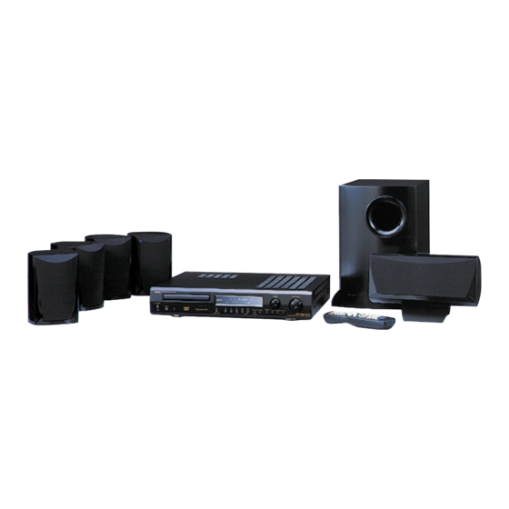
DVD SURROUND RECEIVER
x
ao
y
i
16-11, YUSHIMA 3-CHOME, BUNKYOU-KU, TOKYO 113-0034 JAPAN
http://www.xiaoyu163.com
8
ADV-1000
Q Q
3
6 7
1 3
u163
.
Telephone: 03 (3837) 5321
2 9
9 4
2 8
For Europe model
Hi-Fi Component
1 5
0 5
8
2 9
9 4
m
co
9 9
2 8
9 9
X0146 NC 0207
Advertisement

Related Manuals for Denon ADV-1000


Summary of Contents for Denon ADV-1000
- Page 1 3 7 63 1515 0 For Europe model Hi-Fi Component SERVICE MANUAL ADV-1000 MODEL DVD SURROUND RECEIVER L 13942296513 Some illustrations using in this service manual are slightly different from the actual set. u163 16-11, YUSHIMA 3-CHOME, BUNKYOU-KU, TOKYO 113-0034 JAPAN...
-
Page 2: Safety Precautions
ADV-1000 3 7 63 1515 0 SAFETY PRECAUTIONS The following check should be performed for the continued protection of the customer and service technician. LEAKAGE CURRENT CHECK Before returning the unit to the customer, make sure you make either (1) a leakage current check or (2) a line to chassis resistance check. - Page 3 ADV-1000 3 7 63 1515 0 DIAGNOSTICS OF OPTICAL PICKUP AND REPLACING TRAVERSE UNIT Make failure diagnostics of the Optical Pickup as follows. If the laser drive current becomes more than 1.5 times of the initial value, the Optical Pickup should be replaced.
- Page 4 ADV-1000 3 7 63 1515 0 Note for Handling the Laser Pick-up The protection for the damage of laser diode. If you want to change the optical device unit from any other units, you must keep the following. (1) It should be done at the desk already took measures the static electricity in care of removing the OPU's (Optical device unit) connector cable.
- Page 5 ADV-1000 3 7 63 1515 0 Optical Pick-up Diagnostics and Replacement When repairing, carry out failure diagnostics by following the procedure described below. If the present value of the laser drive current is 50% up to initial value, it is the point of the pickup replacement.
- Page 6 ADV-1000 3 7 63 1515 0 DISASSEMBLY ( Follow the procedure below in reverse order when reassembling ) 1. Top Cover (1) Remove 4 screws on both sides. (2) Remove 6 screws on the rear panel. (3) Remove the top screw (4) Detach the Top Cover to the arrow direction.
- Page 7 ADV-1000 3 7 63 1515 0 3. DVD Mecha. Unit (1) Remove 4 top screws on the DVD Mecha. (2) Disconnect 2 FFCs and 2 pcs of 8P connectors from the DVD Mecha. 8P connector 8P connector 4. Power Supply P.W.B.
- Page 8 ADV-1000 3 7 63 1515 0 5. Back Panel (1) Take off the cord bush. (2) Remove 5 screws and 23 screws 6. Video P.W.B. Disconnect 3 FFCs and 3P connector. Cord bush Video P.W.B. 3P connector L 13942296513 7.
- Page 9 ADV-1000 3 7 63 1515 0 8. Amp P.W.B. (1) Remove the screw and 4 screws " (2) Disconnect FFC and 6P connector. " 6P connector Amp P .W.B. L 13942296513 u163 http://www.xiaoyu163.com...
- Page 10 ADV-1000 3 7 63 1515 0 TRAVERSE UNIT DISASSEMBLY (Follow the procedure below in reverse order when reassembling) Caution: The optical pickup can be damaged easily by static electricity charged on human body. Take necessary anti-static measures when repairing around the optical pickup.
- Page 11 ADV-1000 3 7 63 1515 0 3. Traverse Unit disassembly (1) Remove 24P FFC (CX241), 15P FFC (CX151), 5P PH WIRE (CX051) and 3P PH WIRE (CX031) connecting with from the DVD Main P.W.B. 24P FFC (CX241) (2) Remove 4 screws of fixing Damper.
-
Page 12: Troubleshooting
ADV-1000 3 7 63 1515 0 TROUBLESHOOTING 1. No power (LED doesn't light.) When replacing µcom, µcom Check connector insertion. Re-insert the connector. P. SUPPLY (1U-3434-2): peripheral parts, or Main P.W.B. in [CX171/CX033] servicing, perform initializing of the DSP/AUDIO (1U-3435-3): DVD player. - Page 13 ADV-1000 3 7 63 1515 0 3. DVD no operation (MECHA ERR display) Check connector insertion. Re-insert the connector. P. SUPPLY (1U-3434-2): [CX171/CW035] DVD MAIN (GU-3430): [CX081/CX082] Mecha. Unit: [CX241/CX151/CX051] Check voltage of power wire. Refer to "6. Switching power no output".
- Page 14 ADV-1000 3 7 63 1515 0 4. No video output (Interlace) Check YUV signal. Check soldering of RA125, RA126, Check by replacing IC101 on DVD MAIN Check if signals are output from IC701, and IC101 on DVD MAIN P.W.B.
- Page 15 ADV-1000 3 7 63 1515 0 5. No analog signal output (Audio) Check by replacing IC101 on DVD MAIN Check audio digital signal. Check soldering of chip emi-fil put in Check if signals are output from series to IC101 on DVD MAIN P.W.B.
- Page 16 http://www.xiaoyu163.com AVD-1000 BLOCK DIAGRAM 3 7 6 3 1 5 1 5 0 1U-3443-1 1U-3434-3 VIDEO UNIT SCART UNIT BA7660 MUTE BU4053 MUTE DVD ENGINE UDVD-10 MUTE DVD MECHA FRONT-END CIRCUIT MUTE 1U-3435-1 MUTE DISPLAY UNIT ES4408 MUTE BH7862 BA7660 YUV DATA DVD DECODER DVD DSP...
- Page 17 ADV-1000 3 7 6 3 1 5 1 5 0 LEVEL DIAGRAMS BUFF. PRE AMP POWER AMP DIRECT ANALOG SP OUT 200mV D/AOUT H/P JACK REV. AMP H/P AMP config1: OFF config2: ON FROM S.W SP OUT 40W/6ohm 0dBFS (15.5Vrms)
- Page 18 ADV-1000 3 7 6 3 1 5 1 5 0 D/AOUT LINE LINE POWER FROM SP OUT MUTE PRE OUT 1 3 9 4 2 2 9 6 5 1 3 SP OUT 40W/6ohm 0dBFS (15.5Vrms) -10dBFS 22.17dB WOOFER 7.5dB...
- Page 19 ADV-1000 3 7 6 3 1 5 1 5 0 CLOCK FLOW 1 3 9 4 2 2 9 6 5 1 3 w w w u 1 6 3 http://www.xiaoyu163.com...
- Page 20 ADV-1000 3 7 63 1515 0 SEMICONDUCTORS IC's Note: Abbreviation ahead of IC No. indicates the name of P .W.B. AMP / Power P.W.B. MA: Main P.W.B. Video / Out P.W.B. DM: DVD Main P .W.B. M30624FG (MA: IC302)
- Page 21 ADV-1000 3 7 63 1515 0 Port Name Symbol Function RESERVED(DENON BUS) Arbitration input on DENON BUS (same as serial data) 50/60 Detect input of power pulse (50/60 Hz) FAN ON/OFF Fan motor drive output IN JOGB JOG pulse input B for function switching...
- Page 22 ADV-1000 3 7 63 1515 0 Port Name Symbol Function D14/P16 89055 CSFLAG Signal change detect input from DIR D13/P15 REMOTE IR remote control input D12/P14 /SYR Reset output to RDS IC of tuner D11/P13 INTREQ IN Open drain operation (L: output, H: switch to input)
- Page 23 ADV-1000 3 7 63 1515 0 BD3811K1 (MA: IC504) IN31 TNF2 RECSW RECSW IN32 TNF1 IN41 BNF11 TREBLE IN42 BNF21 INSW IN51 BNF12 BASS IN52 BNF22 IN61 BBNF2 IN62 OUT2 IN71 BBNF1 BASS BOOST IN72 OUT1 Input mute SW...
- Page 24 ADV-1000 3 7 63 1515 0 Pin No. Pin Name Description IN1DSP 1ch DSP input terminal IN1MIX 1ch DSP MIX input terminal IN2DSP 2ch DSP input terminal IN2MIX 2ch DSP MIX input terminal INDSPSR DSP surround Rch input terminal...
- Page 25 ADV-1000 3 7 63 1515 0 ES4408F (DM: IC101) HCS3FX# HCS1FX# HIOCS16# HRD#/DCI_ACK# HWR#/DCI_CLK LA10 LA11 HIORDY LA12 HRST# LA13 HIRQ/DCI_ERR# LA14 HRDQ# LA15 HWRQ#/DCI_REQ# LA16 HD15 HD14 LA17 LA18 HD13 LA19 HD12 LA20 HD11 LA21 HD10 RESET# TDMDX/RSEL...
- Page 26 ADV-1000 3 7 63 1515 0 Pin No. Pin Name Function Pin No. Pin Name Function DMA 3 DRAM address bus YUV 2 8-bit YUV output DMA 4 DRAM address bus YUV 3 8-bit YUV output DMA 5 DRAM address bus...
- Page 27 ADV-1000 3 7 63 1515 0 TP2050 (AP: IC102, 202, 302) Pin No. Pin Name Function 3.6V power supply HA 2 Host address bus VCCSIGN GNDSUB Peripheral protection voltage VCCSIGN OUT2B OUT2B AUX 0 Auxiliary port, (SDATA) I/O VCC2B...
- Page 28 ADV-1000 3 7 63 1515 0 16M SDRAM (TSOP)-8 (DM: IC103, 104) K4S161622D-TC80 W981616AH-8 Terminal Function Pin No. Pin Name Symbol Function Power Supply/Ground Power and ground for the input buffer and the core logic Data Input/Output Data input/output are mutiplexed on the same pin...
- Page 29 ADV-1000 3 7 63 1515 0 M5705 (DM: IC501) AVSS-DS XRD(3) XSRFIN XRD(12) XSIPIN AVDD5-DS XRD(2) XSDSSLV XRD(13) XSRSLINT XRD(1) XRD(14) XSAWRC XRD(0) XSRFGC XRD(15) XSEFGC XHD(7) XSFOCUS XHD(8) XSTRACK XHD(6) XSSLEG XHD(9) AVDD5-DA XHD(5) XSMOTOR XHD(10) AVSS-DA XHD(4)
- Page 30 ADV-1000 3 7 63 1515 0 Pin No. Pin Name Type Description XSSBAD Sub-beam addition signal input Phase detector reference current generator. Connect a resistor between this pin and XSPDIREF ground to set reference current Frequency detector reference current generator. Connect a resistor between this pin and...
- Page 31 ADV-1000 3 7 63 1515 0 Pin No. Pin Name Type Description XHPDIAGJ This pin is used as the Passed Diagnostics signal, and may be an input or an open-drain output This pin is used as the Drive Active/Slave Present signal, and is an input or an open-drain XHDASPJ output.
- Page 32 ADV-1000 3 7 63 1515 0 SP3721A (DM: IC502) DVDRFP SDEN DVDRFN SDATA SCLK TOP VIEW MEVO MLPF L 13942296513 SP3721A Terminal Function Pin No. Type Description Pin Name 1, 2 DVDREP , DVDREN RF Signal Inputs. Differential RF signal attenuator input pins CDRF RF Signal Inputs.
- Page 33 ADV-1000 3 7 63 1515 0 Pin No. Pin Name Type Description Center Error Signal Output. Center error output reference to VCI NEVO SIGO Bottom Envelope Output. Bottom envelope for mirror detection Defect Output. Pseudo CMOS output. When a defect is detected, the DFT output goes high. Also the servo AGC output can be monitored at this pin, when CAR bits 7-4 are ‘0011’...
- Page 34 ADV-1000 3 7 63 1515 0 ADV7172KST (DM: IC701) COMP1 DAC A DAC B TOP VIEW DAC C DAC D CSO_HSO DAC E ADV7172KST Terminal Function Pin No. Pin Name Function P7-P0 8-Bit 4:2:2 Multiplexed YCrCb Pixel Port (P7-P0).
- Page 35 ADV-1000 3 7 63 1515 0 LC89055W (MA: IC713) LC89055W Terminal Function Pin Name Function DISEL Data input terminal (select input pin of DIN0, DIN1) DOUT Input bi-phase data through output terminal DIN0 Amp built-in coaxial/optical input correspond data input terminal...
- Page 36 ADV-1000 3 7 63 1515 0 CS493292-CL (MA: IC720) A0, SCCLK AUDATA2 DATA7, EMAD7, GPIO7 DATA6, EMAD6, GPIO6 DATA5, EMAD5, GPIO5 RESET DATA4, EMAD4, GPIO4 AGND Top View DGND2 FILT1 DATA3, EMAD3, GPIO3 FILT2 DATA2, EMAD2, GPIO2 CLKSEL DATA1, EMAD1, GPIO1...
- Page 37 ADV-1000 3 7 63 1515 0 AK4527BVQ (MA: IC721) SDOS DZF2/OVF RIN+ SMUTE RIN- BICK LIN+ AK4527BVQ LRCK LIN- SDTI1 ROUT1 Top View SDTI2 LOUT1 SDTI3 ROUT2 SDTO LOUT2 DAUX ROUT3 LOUT3 AK4527BVQ Terminal Function Port Name Function SDOS...
- Page 38 ADV-1000 3 7 63 1515 0 TC2000 (AP: IC101, 201, 301) BIASCAP FDBKP2 DCMP BBM1 FDBKN2 BBM2 VPWR MUTE FDBKP1 FDBKN1 HMUTE OVRLDB OCD0 OCD1 L 13942296513 TC2000 Pin Description Pin No. Function Description Bandgap reference times two (typically 2.5VDC). Used to set the common mode voltage for the BIASCAP input op amps.
- Page 39 ADV-1000 3 7 63 1515 0 BH7862FS (VO: IC206) CTRAP COUT 75ohm TEST MUTE1 MUTE1 TEST 1.5-6M 75ohm MIXOUT MIXFB YTRAP CLAMP CLAMP PYIN 75ohm YOUT PYTRAP PYOUT 75ohm PbIN PYFB PrIN PbOUT 75ohm L 13942296513 MUTE2 N.C. MUTE2...
- Page 40 ADV-1000 3 7 63 1515 0 AD1854 (MA: IC401) Terminal Function Pin No. Pin Name Function DGND DVDD DGND Digital Ground. MCLK Master Clock Input. MCLK SDATA CLATCH Latch input for control data. CLATCH BCLK CCLK Control clock input for control data.
- Page 41 ADV-1000 3 7 63 1515 0 74LVX574MTC (MA: IC714) SN74LVC574APW (MA: IC717) logic symbol Function Table (each flip-flop) INPUTS OUTPUT H or L SN74HCT244APW (MA: IC706, 724) SN74LV244APW (MA: IC715) SN74LVC244APW (MA: IC727) logic symbol Function Table INPUTS OUTPUT...
- Page 42 ADV-1000 3 7 63 1515 0 BD6670FM Terminal Function BD6670FM (DM: IC510) Function Name Hall input Amp 1 positive input EXOR H1+ Hall comp Hall input Amp 1 negative input Comp Hall input Amp 2 positive input Hall input Amp 2 negative input...
- Page 43 ADV-1000 3 7 63 1515 0 BA7625 (VO: IC201, 203) BU4053BCF (VO: IC204) BA7626 (VO: IC202) MM74HC08MTC (AP: IC401, 402) Note1: *mark means that feasible for either H or L. Note2: Each input terminal is provided with sink chip clamp (BA7625)/ Each input terminal takes 20kohm at the end (BA7626).
- Page 44 ADV-1000 3 7 63 1515 0 M51957BFP (MA: IC303) PC123 (AP: IC914) Output: Open Collector TOP VIEW µA 25 µA ANODE COLLECTOR Input Output Input Output CATHODE EMITTER Delay-Cap 1.25 V S29590A (MA: IC301) Delay-Cap STR-F6667B (AP: IC901) TEST...
- Page 45 ADV-1000 3 7 63 1515 0 TRANSISTORS 2SC2412K DTA114EK DTA Series DTC Series KTA1504 DTC114EK KTC2875B DTC114YK DTC323TK VIEW VIEW 10kohm 10kohm DTA114EK 10kohm 10kohm DTC114EK 10kohm 47kohm DTC114YK 2.2kohm DTC323TK 2SA988 2SA1015 2SC1740S 2SC1815 2SB1132 2SC2458 2SC4672 2SC3852A...
- Page 46 ADV-1000 3 7 63 1515 0 FL TUBE 15ST36GN (MA: FL101) Pin Assignment Pin No, Connection Pin No, Connection Note: 1. Fn: Filament 2. nG: Grid 3. Pn: Anode L 13942296513 4. NP: No Pin 5. NX: No Connection...
- Page 47 ADV-1000 PRINTED WIRING BOARDS 3 7 6 3 1 5 1 5 0 1U-3434A AMP/POWER P .W.B. UNIT Ass'y 1 3 9 4 2 2 9 6 5 1 3 w w w u 1 6 3 COMPONENT SIDE...
- Page 48 ADV-1000 3 7 6 3 1 5 1 5 0 1U-3434A AMP/POWER P .W.B. UNIT Ass'y 1 3 9 4 2 2 9 6 5 1 3 w w w u 1 6 3 FOIL SIDE http://www.xiaoyu163.com...
- Page 49 ADV-1000 3 7 6 3 1 5 1 5 0 1U-3435A MAIN P .W.B. UNIT Ass'y 1 3 9 4 2 2 9 6 5 1 3 w w w u 1 6 3 COMPONENT SIDE http://www.xiaoyu163.com...
- Page 50 ADV-1000 3 7 6 3 1 5 1 5 0 1U-3435A MAIN P .W.B. UNIT Ass'y 1 3 9 4 2 2 9 6 5 1 3 w w w u 1 6 3 FOIL SIDE...
- Page 51 ADV-1000 3 7 6 3 1 5 1 5 0 GU-3430 DVD MAIN P .W.B. UNIT Ass'y 1 3 9 4 2 2 9 6 5 1 3 w w w u 1 6 3 COMPONENT SIDE http://www.xiaoyu163.com...
- Page 52 ADV-1000 3 7 6 3 1 5 1 5 0 GU-3430 DVD MAIN P .W.B. UNIT Ass'y 1 3 9 4 2 2 9 6 5 1 3 w w w u 1 6 3 FOIL SIDE http://www.xiaoyu163.com...
- Page 53 ADV-1000 3 7 6 3 1 5 1 5 0 1U-3443A VIDEO/OUT P .W.B. UNIT Ass'y 1 3 9 4 2 2 9 6 5 1 3 w w w u 1 6 3 COMPONENT SIDE FOIL SIDE http://www.xiaoyu163.com...
- Page 54 ADV-1000 3 7 63 1515 0 NOTE FOR PARTS LIST Part indicated with the mark " " are not always in stock and possibly to take a long period of time for supplying, or in some case supplying of part may be refused.
- Page 55 ADV-1000 3 7 63 1515 0 PARTS LIST OF P.W.B. UNIT ASS'Y 1U-3434A AMP/POWER P.W.B. UNIT ASS'Y Ref. No. Part No. Part Name Remarks Ref. No. Part No. Part Name Remarks SEMICONDUCTORS GROUP D915-917 276 0432 903 1SS270A TE (TAPE)
- Page 56 ADV-1000 3 7 63 1515 0 Ref. No. Part No. Part Name Remarks Ref. No. Part No. Part Name Remarks R216 247 2010 956 RM73B--203JT R425 247 2009 983 RM73B--103JT R217 247 2018 903 RM73B--0R0KT R426,427 244 2064 961 RS14B3A201JNBST(S)
- Page 57 ADV-1000 3 7 63 1515 0 Ref. No. Part No. Part Name Remarks Ref. No. Part No. Part Name Remarks R956-958 247 2018 903 RM73B--0R0KT C224 257 0032 904 CK73F1H104ZT R960,961 243 2039 032 RW99=3H0R1K C225 254 4618 901 CE04W1H101MT H12(LXZ)
- Page 58 ADV-1000 3 7 63 1515 0 Ref. No. Part No. Part Name Remarks Ref. No. Part No. Part Name Remarks C802,803 254 4213 924 CE04W0J470MT (SRA) C966 257 0511 904 CK73F1H103ZT C804,805 257 0512 903 CK73F1E104ZT C967-969 254 4607 909 CE04W1C471MT H20(LXV)
- Page 59 ADV-1000 3 7 63 1515 0 1U-3435A MAIN P.W.B. UNIT ASS'Y Ref. No. Part No. Part Name Remarks Q'ty Ref. No. Part No. Part Name Remarks L201,202 235 0148 005 INDUCTOR 10UH (DAW) SEMICONDUCTORS GROUP L301,302 235 0148 005 INDUCTOR 10UH (DAW)
- Page 60 ADV-1000 3 7 63 1515 0 Ref. No. Part No. Part Name Remarks Ref. No. Part No. Part Name Remarks TR503,504 275 0100 902 2SK771-5-TB R116 247 2005 945 RM73B--151JT TR505 269 0144 905 DTC114YK-T146 R117 247 2005 961 RM73B--181JT...
- Page 61 ADV-1000 3 7 63 1515 0 Ref. No. Part No. Part Name Remarks Ref. No. Part No. Part Name Remarks R394 247 2005 987 RM73B--221JT R564 247 2012 925 RM73B--104JT R395 247 2010 998 RM73B--303JT R565 247 2018 903 RM73B--0R0KT...
- Page 62 ADV-1000 3 7 63 1515 0 Ref. No. Part No. Part Name Remarks Ref. No. Part No. Part Name Remarks R662 247 2009 983 RM73B--103JT R836 247 2018 903 RM73B--0R0KT R663 247 2010 969 RM73B--223JT R837 247 2011 942 RM73B--473JT...
- Page 63 ADV-1000 3 7 63 1515 0 Ref. No. Part No. Part Name Remarks Ref. No. Part No. Part Name Remarks C358 257 0511 904 CK73F1H103ZT C596-601 257 0506 935 CC73CH1H820JT C359 257 0509 929 CK73B1H102KT C602 254 4541 939 CE04W1E470MT SMG/RE3...
- Page 64 ADV-1000 3 7 63 1515 0 Ref. No. Part No. Part Name Remarks Ref. No. Part No. Part Name Remarks Q'ty C752 257 0512 903 CK73F1E104ZT CX152 205 1100 054 15P FFC BASE (P=1) C753 254 4536 928 CE04W1A101MT SMG/RE3...
- Page 65 ADV-1000 3 7 63 1515 0 1U-3443A VIDEO/OUT P.W.B. UNIT ASS'Y Ref. No. Part No. Part Name Remarks Ref. No. Part No. Part Name Remarks SEMICONDUCTORS GROUP C211-216 254 4522 903 CE04W1V4R7MT SMG/RE3 C217 254 4533 934 CE04W0J221MT SMG/RE3...
- Page 66 ADV-1000 3 7 63 1515 0 GU-3430 DVD MAIN P.W.B. UNIT ASS'Y Ref. No. Part No. Part Name Remarks Q'ty Ref. No. Part No. Part Name Remarks L202,203 235 0070 911 INDUCTOR(220)ST SEMICONDUCTORS GROUP L204 235 0074 991 INDUCTOR(R68)ST...
- Page 67 ADV-1000 3 7 63 1515 0 Ref. No. Part No. Part Name Remarks Ref. No. Part No. Part Name Remarks R138 247 2007 943 RM73B--102JT R558 247 2018 903 RM73B--0R0KT R139-145 247 2018 903 RM73B--0R0KT R567 247 2018 903 RM73B--0R0KT...
- Page 68 ADV-1000 3 7 63 1515 0 Ref. No. Part No. Part Name Remarks Ref. No. Part No. Part Name Remarks R729 247 2007 943 RM73B--102JT C146 257 0509 929 CK73B1H102KT R730 247 2005 987 RM73B--221JT C147-149 257 0512 903 CK73F1E104ZT...
- Page 69 ADV-1000 3 7 63 1515 0 Ref. No. Part No. Part Name Remarks Ref. No. Part No. Part Name Remarks C528 254 4213 937 CE04W0J101MT (SRA) C627 254 4213 937 CE04W0J101MT (SRA) C529 257 0508 959 CC73CH1E681JT C628,629 257 0512 903 CK73F1E104ZT...
- Page 70 ADV-1000 EXPLODED VIEW OF CABINET 3 7 6 3 1 5 1 5 0 WARNING: Parts marked with this symbol have critical characteristics. Use ONLY replacement parts recommended by the manufacturer. 1 3 9 4 2 2 9 6 5 1 3...
- Page 71 ADV-1000 3 7 63 1515 0 PARTS LIST OF EXPLODED VIEW Ref. No. Part No. Part Name Remarks Q'ty Ref. No. Part No. Part Name Remarks Q'ty 1U- 3434 A AMP/POWER UNIT 43A 513 3463 001 LABEL(LASER) AMP UNIT 44 445 8004 007 WIRE CLAMPER P.SUPPLY UNIT...
- Page 72 ADV-1000 EXPLODED VIEW OF DVD MECHANISM 3 7 6 3 1 5 1 5 0 1 3 9 4 2 2 9 6 5 1 3 w w w u 1 6 3...
- Page 73 ADV-1000 3 7 63 1515 0 PARTS LIST OF DVD MECHANISM UNIT Ref. No. Part No. Part Name Remarks Q'ty Ref. No. Part No. Part Name Remarks Q'ty 9KC 1A01 7A MAIN CHASSIS ASS'Y TAPE W10X30 (NITTO NO.156)
- Page 74 ADV-1000 POINTS OF GREASING 3 7 6 3 1 5 1 5 0 With Cemedine 575, glue 3 joint parts of Clamper-L and H hooks. (0.05mg each x 3) *As for greasing to the R rail groove and groove's side edge, apply grease to the outer face "intentionally".
- Page 75 ADV-1000 3 7 63 1515 0 PACKING VIEW L 13942296513 PARTS LIST OF PACKING & ACCESSORIES Ref. No. Part No. Part Name Remarks Q'ty Ref. No. Part No. Part Name Remarks Q'ty 201 505 8092 010 LAMINATE ENVELOPE 212 511 3919 009 INST. MANUAL(E2) 202 504 0205 006 POLYETHYLENE SHEET 213 515 0921 005 S.S.LIST(EX)
- Page 76 ADV-1000 3 7 63 1515 0 MEASURING METHOD AND WAVEFORMS To check the waveforms on the DVD Main P.W.B., the GND ( ) probe of the oscilloscope to Vref point. NOTES Measuring Disc: DVD/DVDT-S01 CD/TCD-784 (It is better to use wires for extending between the probe and test points.) When watching the HF waveform, use the extending wire as short as possible.
- Page 77 ADV-1000 3 7 63 1515 0 WAVEFORMS DVD MAIN P.W.B. DVD PLAY Disk : TDV-520A DVD PLAY (INNER) ⑩EC ⑪FG ①HF(RFO) H1+ Verf Verf Verf Verf A1 CD PLAY Disk : TCD-784 CD PLAY (INNER) ⑩EC ⑪FG H1+ ①HF(RFO)
- Page 78 ADV-1000 3 7 63 1515 0 WIRING DIAGRAM CX171(FFC P=1.00) CY172(FFC P=1.00) RGB_H RGB_H CX153(FFC P=1.00) CY153(FFC P=1.00) VCNT1/YC_H VCNT1/YC_H VCNT2/WIDE VCNT2/WIDE RGB H RGB H +5V_V1 +5V_V1 FUNC SW FUNC SW GND V1 GND V1 GND V1 GND V1 1U-3443-1 N.C.
- Page 79 ADV-1000 SCHEMATIC DIAGRAMS (1/10) 3 7 6 3 1 5 1 5 0 1 3 9 4 2 2 9 6 5 1 3 WARNING: Parts marked with this symbol have critical characteristics. Use ONLY replacement parts recommended by the manufacture.
- Page 80 ADV-1000 SCHEMATIC DIAGRAMS (2/10) 3 7 6 3 1 5 1 5 0 1 3 9 4 2 2 9 6 5 1 3 WARNING: Parts marked with this symbol have critical characteristics. Use ONLY replacement parts recommended by the manufacture.
- Page 81 ADV-1000 SCHEMATIC DIAGRAMS (3/10) 3 7 6 3 1 5 1 5 0 1 3 9 4 2 2 9 6 5 1 3 WARNING: ± B LINE Parts marked with this symbol have critical characteristics. Use ONLY replacement parts recommended by the manufacture.
- Page 82 ADV-1000 SCHEMATIC DIAGRAMS (4/10) 3 7 6 3 1 5 1 5 0 1 3 9 4 2 2 9 6 5 1 3 w w w WARNING: Parts marked with this symbol have critical characteristics. u 1 6 3 Use ONLY replacement parts recommended by the manufacture.
- Page 83 ADV-1000 SCHEMATIC DIAGRAMS (5/10) 3 7 6 3 1 5 1 5 0 1 3 9 4 2 2 9 6 5 1 3 ± B LINE SIGNAL LINE WARNING: Parts marked with this symbol have critical characteristics. Use ONLY replacement parts recommended by the manufacture.
- Page 84 ADV-1000 SCHEMATIC DIAGRAMS (6/10) 3 7 6 3 1 5 1 5 0 1 3 9 4 2 2 9 6 5 1 3 WARNING: Parts marked with this symbol have critical characteristics. Use ONLY replacement parts recommended by the manufacture.
- Page 85 ADV-1000 SCHEMATIC DIAGRAMS (7/10) 3 7 6 3 1 5 1 5 0 1 3 9 4 2 2 9 6 5 1 3 WARNING: ± B LINE Parts marked with this symbol have critical characteristics. SIGNAL LINE Use ONLY replacement parts recommended by the manufacture.
- Page 86 ADV-1000 SCHEMATIC DIAGRAMS (8/10) 3 7 6 3 1 5 1 5 0 1 3 9 4 2 2 9 6 5 1 3 NOTICE ALL RESISTANCE VALUES IN OHM. k=1,000 OHM M=1,000,000 OHM ALL CAPACITANCE VALUES IN MICRO FARAD. P=MICRO-MICRO FARAD EACH VOLTAGE AND CURRENT ARE MEASUERD AT MO SIGNAL INPUT CONDITION.
- Page 87 ADV-1000 SCHEMATIC DIAGRAMS (9/10) 3 7 6 3 1 5 1 5 0 HF(RFO) HOME SW 1 3 9 4 2 2 9 6 5 1 3 w w w WARNING: Parts marked with this symbol have critical characteristics.
- Page 88 ADV-1000 SCHEMATIC DIAGRAMS (10/10) 3 7 6 3 1 5 1 5 0 1 3 9 4 2 2 9 6 5 1 3 WARNING: ± B LINE Parts marked with this symbol have critical characteristics. Use ONLY replacement parts recommended by the manufacture.
Need help?
Do you have a question about the ADV-1000 and is the answer not in the manual?
Questions and answers