
Related Manuals for Akai CFTD2052


Summary of Contents for Akai CFTD2052
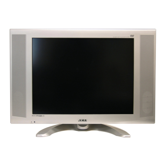
- Page 1 CFTD2052 SERVICE MANUAL LCD COLOR TELEVISION/DVD VIDEO PLAYER ORIGINAL MFR'S VERSION A Design and specifications are subject to change without notice.
-
Page 2: Caution
CAUTION THIS LCD COLOR TELEVISION EMPLOYS A LASER SYSTEM. TO ENSURE PROPER USE OF THIS PRODUCT, PLEASE READ THIS SERVICE MANUAL CARE- FULLY AND RETAIN FOR FUTURE REFERENCE. SHOULD THE UNIT REQUIRE MAINTENANCE, CONTACT AN AUTHORIZED SERVICE LOCATION-SEE SERVICE PROCEDURE. USE OF CONTROLS, ADJUSTMENTS OR THE PERFORMANCE OF PROCEDURES OTHER THAN THOSE SPECIFIED HEREIN MAY RESULT IN HAZARDOUS RADIATION EXPOSURE. -
Page 3: Servicing Notices On Checking
SERVICING NOTICES ON CHECKING 1. KEEP THE NOTICES 6. AVOID AN X-RAY As for the places which need special attentions, Safety is secured against an X-ray by consider- they are indicated with the labels or seals on the ing about the cathode-ray tube and the high cabinet, chassis and parts. -
Page 4: Important Safeguards
IMPORTANT SAFEGUARDS READ INSTRUCTIONS All the safety and operating instructions should be read before the unit is operated. RETAIN INSTRUCTIONS The safety and operating instructions should be retained for future reference. HEED WARNINGS All warnings on the unit and in the operating instructions should be adhered to. FOLLOW INSTRUCTIONS All operating and use instructions should be followed. - Page 5 IMPORTANT SAFEGUARDS (CONTINUED) OUTDOOR ANTENNA GROUNDING If an outside antenna or cable system is connected to the unit, be sure the antenna or cable system is grounded so as to provide some protection against voltage surges and built-up static charges. Section 810 of the National Electrical Code, ANSI/NFPA 70, provides information with respect to proper grounding of the mast and support- ing structure, grounding of the lead-in wire to an antenna discharge unit, size of grounding conductors, location of antenna discharge unit, connection to grounding electrodes, and requirements for the grounding electrode.
- Page 6 EXAMPLE OF ANTENNA GROUNDING AS PER THE NATIONAL ELECTRICAL CODE ANTENNA LEAD IN WIRE GROUND CLAMP ANTENNA DISCHARGE UNIT (NEC SECTION 810-20) ELECTRIC SERVICE EQUIPMENT GROUNDING CONDUCTORS (NEC SECTION 810-21) GROUND CLAMPS POWER SERVICE GROUNDING NEC-NATIONAL ELECTRICAL CODE ELECTRODE SYSTEM (NEC ART 250, PART H) S2898A A1-5...
-
Page 7: Disc Removal Method At No Power Supply
DISC REMOVAL METHOD AT NO POWER SUPPLY Remove the Back Cabinet. (Refer to item 1 of the DISASSEMBLY INSTRUCTIONS.) Slide the Rack Loading toward the arrow direction by hand to release the lock. (Refer to Fig. 1) Take out the Disc from the DVD Deck. Be careful not to scratch on the Disc. DVD Deck Rack Loading Fig. -
Page 8: Table Of Contents
CONTENTS A1-1 CAUTION ........................... A1-2 SERVICING NOTICE ON CHECKING ..................A1-2 HOW TO ORDER PART ......................A1-3~A1-5 IMPORTANT SAFEGUARDS ....................A1-6 DISC REMOVAL METHOD AT NO POWER SUPPLY ............A1-6 PARENTAL CONTROL - RATING LEVEL ................A2-1 CONTENTS ..........................A3-1~A3-6 GENERAL SPECIFICATIONS .................... -
Page 9: General Specifications
GENERAL SPECIFICATIONS LCD Size / Visual Size 20.1 inch / 510.0mmV System LCD Type Color TFT LCD Number of Pixels 640(H) x 480(V) View Range Left/Right 80/80 degree Up/Down 70/70 degree Color System NTSC Speaker 2 Speaker Position Front Size 1.8 x 3.9 inch Impedance 16 ohm... - Page 10 GENERAL SPECIFICATIONS Safety Circuit IC Protector(Micro Fuse) Regulation Safety Radiation Laser DHHS Temperature Operation C ~ +40 Storage C ~ +60 Operating Humidity Less than 80% RH On Screen Menu(TV) Display Menu Type Icon TV Setup Picture Audio Picture Preference Color Temperature Auto Dimmer CH Tuning...
- Page 11 GENERAL SPECIFICATIONS Rating Level Other OSD Language(Set up Language) Output(RGB/Composite) Eject No disc Reading Play Still/Pause Stop Prohibit Mark Step Skip(>>|) Skip(|<<) Random Yes (CD,MP3) Repeat Slow+ Slow- Search+ Search- Jump Resume Title No. Chapter No. Track No. Time Subtitle No. Angle No.
- Page 12 GENERAL SPECIFICATIONS Play Stop Search+ Search- Skip+ Skip- Slow+ Slow- Still/Pause/Step Display/Call TV/DVD Cancel Audio Select Angle Subtitle Top Menu Setup/TV Menu Return DVD Menu Up/ Set+/ CH Up Down/ Set-/ CH Down Left/Select- Right/Select+ Select/Enter Play Mode Marker Input Select Volume + Volume - Repeat A-B...
- Page 13 GENERAL SPECIFICATIONS Down Mix Out (Dolby Digital) (DTS) Surround (Tru Surround) Screen Saver Available Scan Rates (Component) 480i/480p Audio DAC 192kHz / 24bit G-15 Accessories Owner's Manual Language English / Spanish w/Guarantee Card Remote Control Unit Rod Antenna Poles Terminal Loop Antenna Terminal U/V Mixer...
- Page 14 GENERAL SPECIFICATIONS G-18 Weight Net (Approx.) 9.0kg (19.8 lbs) Net w/o Handle, Stand (Approx.) 8.0kg (17.6 lbs) Gross (Approx.) 11.0kg (24.3 lbs) G-19 Carton Master Carton Content --- Sets Material --- / --- Dimensions W x D x H(mm) Description of Origin Gift Box Material Double/White...
-
Page 15: Disassembly Instructions
DISASSEMBLY INSTRUCTIONS 1. REMOVAL OF MECHANICAL PARTS 1-3: BACK CABINET (Refer to Fig. 1-3) AND P.C. BOARDS Remove the 8 screws (1). Remove the screw (2). 1-1: HANDLE (Refer to Fig. 1-1) Remove the screw (3). Remove the 4 screws (1). Remove the Back Cabinet in the direction of arrow. - Page 16 DISASSEMBLY INSTRUCTIONS 1-5: DVD DECK (Refer to Fig. 1-5) 1-6: SIDE PANEL/OPERATION 2 PCB (Refer to Fig. 1-6) Short circuit the position shown in Fig. 1-5 using a Disconnect the following connector: soldering. If you remove the DVD Deck with no soldering (CP2251).
- Page 17 DISASSEMBLY INSTRUCTIONS 1-8: LCD PCB (Refer to Fig. 1-8-B) 1-10: POWER PCB (Refer to Fig. 1-10) Disconnect the following connectors: Disconnect the following connector: (CP102, CP103, CP104, CP802 and CP3805). (CP3802). (Remove CP802 cable as shown Fig. 1-8-A.) Remove the 4 screws (1). Remove the screw (1).
- Page 18 DISASSEMBLY INSTRUCTIONS 1-12: AV PCB (Refer to Fig. 1-12) 1-14: LCD COVER/LCD PANEL (Refer to Fig. 1-14) Remove the 8 screws (1). Disconnect the following connectors: (CP101, CP1001 and CP2201). Remove the LCD Block in the direction of arrow (A). Remove the 6 screws (1).
-
Page 19: Removal Of Dvd Deck Parts
DISASSEMBLY INSTRUCTIONS 2. REMOVAL OF DVD DECK PARTS 2-2: TRAVERSE UNIT ROD/TRAVERSE UNIT HOLDER/ CD DECK/INSULATOR (Refer to Fig. 2-2) 2-1: LOADING MOTOR ASS'Y/START SW PCB ASS'Y/ Remove the screw (1). END SW PCB ASS'Y (Refer to Fig. 2-1-A) Remove the Traverse Unit Rod. Remove the 3 screws (1). - Page 20 DISASSEMBLY INSTRUCTIONS 2-4: DISC L LEVER/DISC STOPPER/LOCKER STOPPER/ 2-6: LINK R ASS'Y/LINK L/LINK MID/LINK SPRING ROLLER GEAR (Refer to Fig. 2-4-A) (Refer to Fig. 2-6) Remove the screw (1). Remove the screw (1). Remove the Disc L Lever and Disc L Lever Spring. Remove the Link Spring.
- Page 21 DISASSEMBLY INSTRUCTIONS 2-8: CLAMPER ASS'Y/DISC GUIDE ARM/DISC R LEVER (Refer to Fig. 2-8-A) Unlock the support (1) and remove the Clamper Ass'y. Unlock the support (2) and remove the Disc Guide Arm. Unlock the support (3) and remove the Disc R Lever. Clamper Ass'y Disc R Lever Disc Guide Arm...
-
Page 22: Removal And Installation Of Flat Package Ic
DISASSEMBLY INSTRUCTIONS REMOVAL AND INSTALLATION OF When IC starts moving back and forth easily after desoldering completely, pickup the corner of the IC using FLAT PACKAGE IC a tweezers and remove the IC by moving with the IC desoldering machine. (Refer to Fig. 3-3.) REMOVAL NOTE Put Masking Tape (cotton tape) around the Flat Pack-... - Page 23 DISASSEMBLY INSTRUCTIONS INSTALLATION When bridge-soldering between terminals and/or the soldering amount are not enough, resolder using a Thin- Take care of the polarity of new IC and then install the tip Soldering Iron. (Refer to Fig. 3-8.) new IC fitting on the printed circuit pattern. Then solder each lead on the diagonal positions of IC temporarily.
-
Page 24: Service Mode List
SERVICE MODE LIST This unit is provided with the following SERVICE MODES so you can repair, examine and adjust easily. To enter to the SERVICE MODE function, press and hold both buttons simultaneously on the main unit and on the remote control for more than the standard time in the appropriate condition. -
Page 25: When Replacing Eeprom (Memory) Ic
WHEN REPLACING EEPROM (MEMORY) IC If a service repair is undertaken where it has been required to change the MEMORY IC, the following steps should be taken to ensure correct data settings while making reference to TABLE 1. NOTE: No need to set data for between position INI 10 and INI 4F due to the adjustment value. Table 1 Turn on the POWER, and set to the TV mode. -
Page 26: Electrical Adjustments
ELECTRICAL ADJUSTMENTS BEFORE MAKING ELECTRICAL FUNCTION FUNCTION ADJUSTMENTS DRI1 W RCUT M DRI2 W Read and perform these adjustments when repairing the GCUT M MD6 W circuits or replacing electrical parts or PCB assemblies. BCUT M DTHON W DRI1 M DRREF W CAUTION DRI2 M... - Page 27 ELECTRICAL ADJUSTMENTS 2. BASIC ADJUSTMENTS 2-1: Confirmation of Fixed Value (Step No.) Please check if the fixed values of each the adjustment items are set correctly referring below. (RF/AV/DVD/COMPONENT MODE) FUNCTION STEP NO. COMPONENT RCUT M GCUT M BCUT M DRI1 M DRI2 M MD6 M...
-
Page 28: Power
ELECTRICAL ADJUSTMENTS 3. ELECTRICAL ADJUSTMENT PARTS LOCATION GUIDE (WIRING CONNECTION) BACK LIGHT PCB CD7001 LCD PANEL POWER PCB CD503 CD2601 CD2302 CD2301 DVD PCB S3601 S3602 CP2301 CD3601 CP2302 AC IN LCD PCB CP2601 CD501 CD701 CD103 DVD DECK CD102 CD807 CD804 CP101... -
Page 29: Dvd Block Diagram
DVD BLOCK DIAGRAM 8M FLASH 64M SDRAM IC4005 IC4007 HY57V641620HGT-7 SST39VF800A-70-4C-EKE TV BLOCK SDA0~SDA11 HD0~HD15 SDD0~SDD15 HA0~HA20 MECHA A, B, C, D, E, F VR-DVD/CD, VRSEL, VREF LD-DVD/CD, PD Pick RFA_SDEN, DATA, SCLK TR+/–, FO+/– AAF_CE, FE, TE, PI DISC_IN/DISC_END SW READ CHANNEL Open/ IC2601... - Page 30 TV BLOCK DIAGRAM SP1001 AUDIO VIDEO SG04H02CRA SOUND AMP 2.5W IC905 IC1002 STEREO IC903 TUNER 2 IN 1 IC906 LA4915-E IC901 IC904 TU001 NJM2534V MM1501XNRE AN5832SA- 115-V-LA35AR SP1002 (TE2) MIXER SG04H02CRA IC1004 TONE CONTROL 2.5W NJM4580V TUNER IC1001 Audio Out (TE1) VIDEO AN5891SA-E1V...
-
Page 31: Power Block Diagram
POWER BLOCK DIAGRAM DVD BLOCK AV BLOCK Q3001 Q3007 F3001 ADAPTER+12V P.CON+7V_D UNREG+12V 5V REG IC3003 P.CON+5V_D KIA78D05F DVD POWER-H P.CON+A5V_D Q3008 P.CON+3.3V_D 1.8V REG IC3002 P.CON+1.8V_D PQ070XZ01ZPH 2CH SW REG CONTROLLER IC3001 BA9743AFV-E2 5V REG ADAPTER+12V AT+5V IC3803 KIA78D05F Q3801 32V REG P.CON+5V... - Page 32 TV POWER BLOCK DIAGRAM TRANSFORMER SWITCHING D3606 T3601 L3603 CD503 D3603 AC IN L3604 F3601 L3605 D3607 IC3602 PS2561AL1-1-V(W) Q3601 SWITCHING FEED BACK CONTROL IC IC3603 ICE1QS01...
- Page 33 PRINTED CIRCUIT BOARDS LCD (TOP SIDE) LCD (BOTTOM SIDE) TEDB66B TEDB66B L817 C821 C879 L821 W811 C806 C880 C831 C822 L819 C892 C893 C843 C895 C891 C894 C890 C820 IC807 C871 W810 D801 C896 C856 R832 R801 C887 C886 C812 R831 C884 C818...
-
Page 34: Printed Circuit Boards
PRINTED CIRCUIT BOARDS DVD/OPERATION2 (TOP SIDE) VMD327A CP2251 Q2602 CD701 R2617 C2639 R2616 C8512 D2602 R2654 R2618 D8508 C2638 Q2601 IC8502 R2601 W818 Q3002 W819 L8503 W820 R2615 C2630 R2646 C2655 R2645 R4020 R2610 C2617 R4019 C2618 Q3001 R4052 CD501 C2623 R4051 C2607... -
Page 35: Av/Remocon/Side Jack/Operation1
PRINTED CIRCUIT BOARDS AV/REMOCON/SIDE JACK/OPERATION1 (INSERTED PARTS) SOLDER SIDE CD2201 SW2202 SW2208 SW2204 SW2206 W074 SW2209 CD101 W834 W835 W854 TEDB64B CD2251 TEDB63B J792 J790 J791 TEDB65B C2205 OS2201 CD705 D3806 J702 B3802 R3818 J704 J708 J707 J705 AS MARKED. W115 J706 J701... - Page 36 PRINTED CIRCUIT BOARDS AV/REMOCON/SIDE JACK/OPERATION1 (CHIP MOUNTED PARTS) SOLDER SIDE R765 Q701 R704 Q703 Q702 IC701 Q707 Q704 R721 IC904 Q710 Q708 IC903 Q1008 R775 R776 R1048 IC103 Q1006 R770 Q1001 TMD611B IC704 R144 R135 Q105 R134 R772 R773 W910 R901 IC703 IC901...
- Page 37 PRINTED CIRCUIT BOARDS POWER BACK LIGHT (TOP SIDE) BACK LIGHT (BOTTOM SIDE) SOLDER SIDE CD3601_2 RISK OF FIRE - REPLACE AS MARKED . TEDB53B TEDB52A S3602 R3602 CP7004 CP7005 CP7006 L3601 L3602 D7015 T7015 T7019 T7014 T7013 R7062 C3604 R3601 C3623 R3620 T7009...
-
Page 38: Mpeg/Micon/Dsp
MPEG/MICON/DSP SCHEMATIC DIAGRAM (DVD PCB) FROM/TO AUDIO/VIDEO DAC_VIDEO_C C4038 DAC_VIDEO_B DAC_VIDEO_A 0.01 B ASDATA0 ABCLK ALRCLK C4088 R4002 75 +-1% AMCLK 0.01 B R4003 75 +-1% DUPTD1 C4089 R4004 75 +-1% DUPRD1 RESET 0.01 B R4005 75 +-1% SYS_MUTE DUPTD0 C4090 SPDIF DUPRD0... -
Page 39: Memory2
MEMORY2 SCHEMATIC DIAGRAM (DVD PCB) FROM/TO MPEG/MICON/DSP SD_A0 SD_A1 FLASH IC SD_A2 IC4007 SST39VF800A-70-4C-EKE SD_A3 SD_A4 HA16 HA15 SD_A5 SD_A6 SD_A7 C4064 HA14 SD_A8 VCCQ SD_A9 0.1 F 64M SDRAM IC SD_A10 HA13 IC4005 HY57V641620HGT-7 SD_A11 SD_D0 SD_D1 HD15 HA12 SD_D2 DQ15 SD_D3... -
Page 40: Rf Amp
RF AMP SCHEMATIC DIAGRAM (DVD PCB) FROM/TO MPEG/MICON/DSP CD2601 R2633 RFA_SDEN P.CON+3.3V_D RFA_DATA 4.7K RFA_SCLK 2H0O1902 AAF_CE FFC(P=0.5mm) VR_SEL AAF_FE AAF_TE TURN LOGIC AAF_PI Q2606 VR DVD CTL R2620 VR_SEL FROM/TO LOADER DTC124EKA Q2603 2SK3018 R2647 4.7K 4.7K CP2601 VBIASS0 09-5000-024-001-001 VR CD CTL R2623... - Page 41 AUDIO/VIDEO SCHEMATIC DIAGRAM (DVD PCB) C8522 DAC_C[U]C_VIDEO 6.3V C8523 DAC_B[V]Y_VIDEO 6.3V C8524 DAC_A[Y]_VIDEO FROM/TO MPEG/MICON/DSP 6.3V DAC_VIDEO_C DAC_VIDEO_B DAC_VIDEO_A RESET C8505 DAC_VIDEO_C 12P CH AMCLK ABCLK L8502 ALRCLK ASDATA0 0305 SYS_MUTE DUPTD1 C8508 W819 DAC_VIDEO_B DUPRD1 12P CH L8503 SPDIF 0305 C8511 W820...
-
Page 42: Motor Drive
MOTOR DRIVE SCHEMATIC DIAGRAM (DVD PCB) R2314 R2316 R2347 R2351 5.6K +-1% 5.6K +-1% 5.6K +-1% HS76 HS2301 763WSA0031 TO RF AMP JG009 TRACKING CONTROL R2320 100K R2319 R2331 C2305 C2306 C2309 R2304 0.1 B 0.1 B 0.1 B SPINDLE_PWM JG011 SPINDL CONTROL R2303 5.1K... -
Page 43: Regulator2
REGULATOR2 SCHEMATIC DIAGRAM (DVD PCB) FROM/TO AUDIO/VIDEO DVD_POWER_H FROM POWER P.CON+5V_D P.CON+3.3V_D CD501 (CP3804) 5A 32V L3004 DVD_POWER_H CU241401 F3001 ADAPTER+12V (GND,D_GND) 22uH 1206FA5A-T ADAPTER+12V TSL0808 5A32V SBPSC-11R310-101A L3001 P.CON+7V_D TO MOTOR DRIVE 100uH P.CON+A5V_D REG+5V IC P.CON+7V_D IC3003 KIA78D05F Q3001 P.CON+3.3V_D 2SB1132... -
Page 44: Operation2
OPERATION2 SCHEMATIC DIAGRAM (OPERATION 2 PCB) TO OPE./AV JACK/REMOCON R2251 R2252 R2253 R2254 R2255 1.5K 2.7K 6.8K CP2251 (CD2251) A2001WR2-2P KEY1 PCB280 VEDA45A NOTE:THE DC VOLTAGE AT EACH PART WAS MEASURED NOTE:THIS SCHEMATIC DIAGRAM IS THE LATEST AT THE TIME WITH THE DIGITAL TESTER WHEN THE COLOR BROADCAST OF PRINTING AND SUBJECT TO CHANGE WITHOUT NOTICE WAS RECEIVED IN GOOD CONDITION AND PICTURE IS NORMAL. - Page 45 TUNER/STEREO SCHEMATIC DIAGRAM (AV PCB) FROM/TO MICON L901 P.CON+5V_A R CH SW IC 100uH 0305 IC903 MM1501XNRE R904 C941 Vin1 1.2K AV_SW1 AV_SW2 V.OUT TV/DVD C942 Vin2 C916 L CH SW IC TO SOUND AMP IC904 MM1501XNRE R903 C943 TV/DVD SW_A_OUT_L Vin1 TU001...
- Page 46 MICON SCHEMATIC DIAGRAM (AV PCB) FROM/TO IN/OUT IIC_OFF START_SW DVD_RESET DVD_POWER CVBS1 CVBS2/Y SW_U SW_V S_IN_C AV_SW1 S_SW AV_SW2 X101 TO DECODER CSTLS16M0X53-A0 CP103 (CP806) 00_6232_007_006_800 S_IN_C C120 100P CH CD103 R140 LCDON OSD_Y LCDON 2H073601 C103 C121 SW_U 39P CH 100P CH C109 R144...
- Page 47 SOUND AMP SCHEMATIC DIAGRAM (AV PCB) L1003 R1053 HF70T22*10*14 8.21 CD1001 SPEAKER POWER GND OUT1- CU147801 C1002 CP1001 A2502WV2-4P SP1002 8.21 R1026 SG04H02CRA OUT1+ SP OUT R+ 16 OHM 4.7K SP GND R1004 C1003 IN-VREF SP GND SPEAKER SP OUT L+ SP1001 SG04H02CRA PRE VCC...
-
Page 48: In/Out
IN/OUT SCHEMATIC DIAGRAM (AV PCB) AV2_V_IN R709 FROM/TO OPE./AV JACK/REMOCON 100 1/2W R702 C716 W832 S_IN_Y S_VIDEO BUFFER CP705 (CD705) 8.2K J706 Q702 A2001WV2-8P FROM/TO MICON MDC-070V-A_LF KTC3875S_Y_RTK BUFFER AV2_V_IN Q701 CVBS1 KTC3875S_Y_RTK AV2_A_IN_L R701 C717 CVBS2/Y AV2_A_IN_R SW_U 8.2K AV2_A_IN_L W911 SW_V... -
Page 49: Power
POWER SCHEMATIC DIAGRAM (AV PCB) TO SOUND AMP SOUND+B FROM TV POWER AT+5V P.CON+5V CP3802 (CD503) P.CON+9V A3963WV2-3P SOUND_GND FROM/TO MICON FROM/TO MICON LCDON TO INVERTER POWER_ON_H AT+5V C3826 CP3803 (CD7001) P.CON+5V A2001WV2-8P 0.22 B RESET LCD ON/OFF C3827 P.CON9V REG IC I-PWM IC3804 0.22 B... -
Page 50: Operation/Av Jack/Remocon
OPERATION/AV JACK/REMOCON SCHEMATIC DIAGRAM (SIDE JACK PCB) J1001 HSJ0913-01-140 (REMOCON PCB) W835 W834 OS2201 RPM7138-SH8 Vout L713 HF70T22*10*14 FROM/TO IN/OUT YELLOW J790 CD705 (CP705) MTJ-032-05A-30-FE CU281601 HEAD PHONE R+ HEAD PHONE L+ WHITE J791 SP MUTE MTJ-032-05A-32-FE FROM/TO MICON AV2_A_IN_R CD2201 (CP2201) CU251801... -
Page 51: Decoder
DECODER SCHEMATIC DIAGRAM (LCD PCB) CVBS1/CVBS2/Y P.CON+5V FROM/TO POWER CCD_SW (CP3805) CD804 AV SW IC CU262501 IC601 MM1504XNRE BUFFER P.CON+5V C676 Q604 CVBS1 Vin1 KTC3875S_Y_RTK R618 V.OUT C677 CVBS2/Y Vin2 P.CON+3.3V P.CON2.5V REG IC P.CON3.3V REG IC IC804 PQ070XZ01ZPH P.CON+5V IC806 KIA78D33F BUFFER... -
Page 52: Scaler1
SCALER1 SCHEMATIC DIAGRAM (LCD PCB) SCALER IC IC801 (3/5 SCALER) TC90288XBG SCALER IC TO LVDS IC801 (2/5 NOT CONNECT) TC90288XBG R801 NC_A3 NC_V1 PCCK_IN ENAB D-EN_2 NC_A6 NC_V3 PCH_IN NC_A7 NC_V4 PCV_IN LCD_HD NC_A22 NC_W22 NC_A23 NC_Y26 LCD_VD NC_A24 NC_AA2 PCR_IN[7] NC_B3 NC_AA3... -
Page 53: Scaler2
SCALER2 SCHEMATIC DIAGRAM (LCD PCB) SCALER IC IC801 (4/5 DRAM VDD) TC90288XBG NLCV32 L821 P.CON+3.3V W810 D_1.5V TST2_IN[4] DIG_CLK_OUT 22uH TST2_IN[3] DIG_HD_OUT C821 TST2_IN[2] DIG_VD_OUT C820 TST2_IN[1] DIG_FIELD_OUT TST2_IN[0] SCALER IC IC801 (5/5 SCALER VDD) DIG_OUT[7] TC90288XBG TSTD_IN[15] DIG_OUT[6] C896 0.1 B C822 0.1 B TSTD_IN[14] DIG_OUT[5]... -
Page 54: Lvds
LVDS SCHEMATIC DIAGRAM (LCD PCB) TO LCD PANEL For CHIMEI 14"20" Panel CP802 04_6240_050_003_800 FROM SCALER 1 D-EN_2 DCLK D-EN_2 B802 DCLK DCLK DRE7_2 HCB2012K-600T25 DRE6_2 DRE5_2 DRE7_2 DRE4_2 DRE6_2 DRE3_2 DRE2_2 DRE5_2 DRE1_2 DRE4_2 DRE0_2 DGE7_2 DGE6_2 DRE3_2 DGE5_2 DRE2_2 DGE4_2 DGE3_2... -
Page 55: Tv Power
TV POWER SCHEMATIC DIAGRAM (POWER PCB) R3605 0.22 1W L3603 COIL,LINE FILTER 10uHTSL0808 COIL,LINE FILTER L3601 L3602 SS24H-10100 SS24H-10100 T3601 WHITE S3601 8134001S L3607 WHITE BLACK S3602 D3603 HF70T22*10*14 BLACK AC120V_60Hz F3601 D4SB80 173.8 B3602 C3612 CD3601_2 09415911 W5RH3.5X5X1.0 500V 0.001 6.3A125V TO POWER... -
Page 56: Inverter
INVERTER SCHEMATIC DIAGRAM T7013 AV-HB253T R7091 R7085 R7079 R7073 R7067 R7061 R7055 R7049 R7043 R7037 R7114 R7119 R7031 680K 680K 680K 680K 7.5K +-1% (BACK LIGHT PCB) 680K 680K 680K 680K 680K 680K 680K 680K 1/10W 1/10W 1/10W 1/10W 1/10W 1/10W 1/10W 1/10W... -
Page 57: Start Sw/End Sw
START SW/END SW SCHEMATIC DIAGRAM DECK CD M2301 CV-VTM101A MDN3BT3ESA 04_6232_104_015_800 2H091902 STEPPING_MOTOR[B-] STEPPING MOTOR(B-) STEPPING_MOTOR[B+] STEPPING_MOTOR(B+) STEPPING_MOTOR[A-] STEPPING_MOTOR(A-) STEPPING_MOTOR[A+] STEPPING_MOTOR(A+) S2001Y LOADING_MOTOR[+] S2004Y DISC_END_SW S2002Y LOADING_MOTOR[-] S2003Y DISC_IN_SW ESE22MH22 PCB580 DED023 PCB590 (START SW PCB) DED024 ESE22MH24 (END SW PCB) NOTE:THIS SCHEMATIC DIAGRAM IS THE LATEST AT THE TIME NOTE:THE DC VOLTAGE EACH PART WAS OF PRINTING AND SUBJECT TO CHANGE WITHOUT NOTICE... -
Page 58: Interconnection Diagram
INTERCONNECTION DIAGRAM CD3601_2 WHITE S3601 POWER PCB PCB240 BLACK S3602 TEDB53 L3606 H NC H NC H NC H NC H NC H NC CD503 CP3802 CD2601 5 6 7 CP701 CD701 CP2601 L3607 DVD POWER DVD POWER DVD_RESET DVD_RESET YELLOW WHITE BLUE... -
Page 59: Waveforms
WAVEFORMS MPEG/MICON/DSP AUDIO/VIDEO MOTOR DRIVE 10ns 500µs 1.0V 500mV 1.0V REGULATOR 2 500µs 2µs 200ns 2.0V 500mV 500mV MEMORY2 200µs 10µs 2µs 500mV 200mV 2.0V RF AMP TUNER/STEREO 10µs 200ns 100mV 200mV 0.5V 200ns 10µs 200mV 100mV 0.5V The following waveforms were measured at the point of the corresponding NOTE: balloon number in the schematic diagram. -
Page 60: Sound Amp
WAVEFORMS 50ns 50µs 200mV 1.0V 1.0V 10µs 0.5ms 1.0V 200mV 1.0V 10µs 50µs 200mV 1.0V 1.0V 10µs 200mV 1.0V 1.0V MICON SOUND AMP 10µs 20µs 0.5V 1.0V 50mV The following waveforms were measured at the point of the corresponding NOTE: balloon number in the schematic diagram. - Page 61 WAVEFORMS DECODER 0.1µs 50µs 50mV 100mV 0.5V TUNER/STEREO 10µs 10µs 200mV 0.5V 0.5V 10µs 200mV 0.5V IN/OUT 10µs 0.5V 0.5V 50µs 0.5V 0.5V The following waveforms were measured at the point of the corresponding NOTE: balloon number in the schematic diagram.
-
Page 62: Mechanical Exploded Views
MECHANICAL EXPLODED VIEW 118 207 104B 104B 104A 104B 104B 105B 105A 104B 102B 102C 102A 102D 102E PCB280 (OPERATION 2 PCB ASS'Y) 103B PCBDA0 103C (REMOCON PCB ASS'Y) SP1001 103A 101B 101A 101C 101C 101D 101C 101C 101C SP1002 I1-1... - Page 63 MECHANICAL EXPLODED VIEW PCBD90 (SIDE JACK PCB ASS'Y) PCB240 (POWER PCB ASS'Y) PCB130 (DVD PCB ASS'Y) PCBD20 (AV PCB ASS'Y) PCB350 (BACK LIGHT PCB ASS'Y) PCB270 PCB340 (OPERATION 1 PCB ASS'Y) (LCD PCB ASS'Y) I1-2...
-
Page 64: Dvd Deck Exploded Views
DVD DECK EXPLODED VIEW (TOP VIEW) NOTE: Applying positions AA and AB for the grease are CLASS PART NO. PART NAME MARK displayed for this section. GREASE Y315061000 G-555G Check if the correct grease is applied for each p osition. Y315121000 SF-112 I2-1... - Page 65 DVD DECK EXPLODED VIEW (BOTTOM VIEW) PCB580 (START SW PCB ASS'Y) PCB590 M2301 (END SW PCB ASS'Y) NOTE: Applying positions AA and AB for the grease are CLASS PART NO. PART NAME MARK displayed for this section. GREASE Y315061000 G-555G Check if the correct grease is applied for each p osition.
-
Page 66: Mechanical Replacement Parts List
MECHANICAL REPLACEMENT PARTS LIST REF. NO. PART NO. DESCRIPTION REF. NO. PART NO. DESCRIPTION 7A701A466A FRONT,CABI ASS'Y 8110630A0U SCREW,TAP TITE(P) BRAZIER 3x10 101A 701WPJD066 CABINET,FRONT 811063080U SCREW,TAP TITE(P) BRAZIER 3x8 101B 713WPA0291 GLASS,LED 8109230A0U SCREW,TAP TITE(B) BIND 3x10 101C 800WQ0A008 FELT,SHEET 150x5 T=0.3 810763060U SCREW,TAP TITE(S) -
Page 67: Dvd Deck Replacement Parts List
DVD DECK REPLACEMENT PARTS LIST REF. PART NO. DESCRIPTION ! 600 A5N005C650S DVD MECHA ASS'Y A5N005C650S 92AAA0015A ARM ROLLER ASS'Y 2 92AAA0006A LINK,R ASS'Y 92AAA0007A CLAMPER ASS'Y 92AAA0009A MOUTH ASS'Y 92P100041A ARM, DISC GUIDE 92P100044A GEAR, MID RACK 92P100045A GEAR, TERMINAL 92P100046A GEAR, MID ROLLER 1 92P100047A... -
Page 68: Electrical Replacement Parts List
ELECTRICAL REPLACEMENT PARTS LIST REF. NO. PART NO. DESCRIPTION REF. NO. PART NO. DESCRIPTION RESISTORS ! R1050 R3X28B2R7J R,METAL OXIDE 2.7 OHM 3W IC199 A5N103AD25 INIT DATA S-24C08AFJA-TB-0 ! R1053 R3X28B1R8J R,METAL OXIDE 1.8 OHM 3W ICRJ008AN0 IC AT24C08AN-10SI-2. ! R3601 R002T2155J 1.5M OHM 1/2W IC601... - Page 69 ELECTRICAL REPLACEMENT PARTS LIST REF. NO. PART NO. DESCRIPTION REF. NO. PART NO. DESCRIPTION TRANSISTORS COILS &TRANSFORMERS Q3006 TAAA1504SY TRANSISTOR SILICON KTA1504S_Y_RTK L7007 02A6B2E0A1 CORE,FERRITE HF70T22*10*14 ! Q3007 TJ5M081090 FET TPC8109(T2LORION_Q) L8502 02167F1R0K COIL ! Q3008 TJ5M081090 FET TPC8109(T2LORION_Q) L8503 02167F1R0K COIL ! Q3601 T250035680...
- Page 70 ELECTRICAL REPLACEMENT PARTS LIST REF. NO. PART NO. DESCRIPTION REF. NO. PART NO. DESCRIPTION MISCELLANEOUS MISCELLANEOUS B3804 024HT03564 CORE,BEADS W4BRH3.5X6X1.0 ! SP1002 070C546009 SPEAKER SG04H02CRA B3805 024HT03553 CORE,BEADS W5RH3.5X5X1.0 TM101 076R0HE02B TRANSMITTER R56-0516 B4001 024HC31022 CORE,BEADS FCM2012H-102T04 ! TU001 0162300045 RF UNIT 115-V-LA35AR B4002...
- Page 71 M5N1-06A SPEC.NO. W555001 O/R NO.
Need help?
Do you have a question about the CFTD2052 and is the answer not in the manual?
Questions and answers