
Subscribe to Our Youtube Channel
Related Manuals for Aaeon OMNI-2155


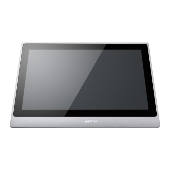
Summary of Contents for Aaeon OMNI-2155
- Page 1 OMNI-2155 Expandable HMI Panel PC User’s Manual 2 Last Updated: October 21, 2015...
- Page 2 Copyright Notice This document is copyrighted, 2015. All rights are reserved. The original manufacturer reserves the right to make improvements to the products described in this manual at any time without notice. No part of this manual may be reproduced, copied, translated, or transmitted in any form or by any means without the prior written permission of the original manufacturer.
- Page 3 Acknowledgement All other products’ name or trademarks are properties of their respective owners. ® is trademark of Advanced Micro Devices. ® Microsoft Windows is a registered trademark of Microsoft Corp. ITE is a trademark of Integrated Technology Express, Inc. ...
- Page 4 Packing List Before setting up your product, please make sure the following items have been shipped: Item Quantity OMNI-2155 Phoenix power connector Product CD with User’s Manual (in pdf) and drivers If any of these items are missing or damaged, please contact your distributor or sales representative immediately.
- Page 5 About this Document This User’s Manual contains all the essential information, such as detailed descriptions and explanations on the product’s hardware and software features (if any), its specifications, dimensions, jumper/connector settings/definitions, and driver installation instructions (if any), to facilitate users in setting up their product. Users must refer to the latest version of this document.
- Page 6 Safety Precautions Please read the following safety instructions carefully. It is advised that you keep this manual for future references All cautions and warnings on the device should be noted. Make sure the power source matches the power rating of the device. Position the power cord so that people cannot step on it.
- Page 7 If any of the following situations arises, please the contact our service personnel: Damaged power cord or plug Liquid intrusion to the device iii. Exposure to moisture Device is not working as expected or in a manner as described in this manual The device is dropped or damaged Any obvious signs of damage displayed on the device...
- Page 8 FCC Statement This device complies with Part 15 FCC Rules. Operation is subject to the following two conditions: (1) this device may not cause harmful interference, and (2) this device must accept any interference received including interference that may cause undesired operation. Caution: There is a danger of explosion if the battery is incorrectly replaced.
- Page 9 China RoHS Requirements (CN) 产品中有毒有害物质或元素名称及含量 AAEON Panel PC/ Workstation 有毒有害物质或元素 部件名称 铅 汞 镉 六价铬 多溴联苯 多溴二苯醚 (Pb) (Hg) (Cd) (Cr(VI)) (PBB) (PBDE) 印刷电路板 × ○ ○ ○ ○ ○ 及其电子组件 外部信号 × ○ ○ ○ ○ ○ 连接器及线材 外壳...
- Page 10 China RoHS Requirement (EN) Poisonous or Hazardous Substances or Elements in Products AAEON Panel PC/ Workstation Poisonous or Hazardous Substances or Elements Hexavalent Polybrominated Polybrominated Component Lead Mercury Cadmium Chromium Biphenyls Diphenyl Ethers (Pb) (Hg) (Cd) (Cr(VI)) (PBB) (PBDE) PCB & Other ○...
-
Page 11: Table Of Contents
Table of Contents Chapter 1 - Product Specifications ..................1 Specifications ......................2 OMNI Modules ......................6 1.2.1 USB/ COM/ LAN Module ..............6 1.2.2 Dual LAN Module ................. 6 1.2.3 MiniCard and SIM Card Module............7 1.2.4 RS-232/422/485 Module ..............7 1.2.5 Isolated RS-232/422/485 Module ............. - Page 12 2.3.5 Board to Board Connector (CN11) ..........21 2.3.6 LVDS Backlight Connector (CN17) ..........22 2.3.7 Mini PCIe Slot (CN18) ................ 23 2.3.8 SATA Power Connector (CN19) ............25 2.3.9 SATA Connector (CN20) ..............25 2.3.10 LVDS Connector (CN21)..............25 2.3.11 HDMI Connector (CN22) ..............
- Page 13 3.4.6.1 Super IO Management: Serial Port 1 Configuration ..46 3.4.6.2 Super IO Management: Serial Port 2 Configuration ..47 3.4.6.3 Super IO Management: Serial Port 3 Configuration ..48 3.4.6.4 Super IO Management: Serial Port 4 Configuration ..49 3.4.6.5 Super IO Management: Serial Port 5 Configuration ..
-
Page 14: Chapter 1 - Product Specifications
Chapter 1 Chapter 1 - Product Specifications... -
Page 15: Specifications
Specifications System ® ® Intel Celeron J1900, 2 GHz Processor ® Intel Atom™ N2807, 1.58 GHz 204-pin DDR3L 1333 MHz SODIMM x 1, up to System Memory 8 GB, (J1900) 204-pin DDR3L 1333 MHz SODIMM x 1, up to 4 GB, (N2807) I0/100/1000Base-TX, RJ-45 x 2 Ethernet... - Page 16 -20°C~55°C with industrial grade device (with 0.5 m/s air flow, according to IEC68-2-14, CPU: J1900) *Users should use wide temperature DRAM and wide temperature storage devices if OMNI-2155 is operating above 40°C. -20 ~ 70°C (-4 ~ -158°F) Storage Temperature ...
- Page 17 Anti-Vibration 1 Grms/ 5 ~ 500 Hz/ Operation (HDD) Anti-Shock 15 G peak acceleration (11 msec. duration) CE/FCC Class A Chapter 1 – Product Specifications...
- Page 18 Power Supply 9 ~ 30 V DC Input 15.6” TFT LCD, LED Display Type 1366 x 768 Max. Resolution 16.7M colors (6/8-bit for R, G, B) Max Colors 400 nits Luminance (cd/m 170° (H), 160° (V) Viewing Angle ...
-
Page 19: Omni Modules
OMNI Modules Featuring a modular designed, the OMNI-2155 can be fitted with a number of modules to expand its base capabilities. Please refer to the sections below for their features. 1.2.1 USB/ COM/ LAN Module Features USB 2.0 x 2 ... -
Page 20: Minicard And Sim Card Module
1.2.3 MiniCard and SIM Card Module Features MiniCard x 2 SIM Card x 2 1.2.4 RS-232/422/485 Module Features RS-232/422/485 x 4 (Selectable by jumper) Chapter 1 – Product Specifications... -
Page 21: Isolated Rs-232/422/485 Module
1.2.5 Isolated RS-232/422/485 Module Features Isolated RS-232/422/485 x 4 (Selectable by jumper) 2k Vdc Isolation 1.2.6 Digital I/O Module Features Digital I/O x 8 1.2.7 CAN Bus Module Features CAN Bus with Phoenix connectors 2k Vdc Isolation ... -
Page 22: Audio Module
1.2.8 Audio Module Features Mic-in Line-out Chapter 1 – Product Specifications... -
Page 23: Chapter 2 - Hardware Information
Chapter 2 Chapter 2 – Hardware Information... -
Page 24: Dimensions
Dimensions Main Panel Chapter 2 – Hardware Information... - Page 25 OMNI Modules USB/ CAN/ LAN Module Dual LAN Module MiniCard & SIM Card Module RS-232/422/485 Module Chapter 2 – Hardware Information...
- Page 26 Isolated RS-232/422/485 Module Digital I/O Module CAN Bus Module Audio Module Chapter 2 – Hardware Information...
-
Page 27: List Of Jumpers
List of Jumpers Please refer to the table below for all of the board’s jumpers that you can configure for your application Label Function Clear CMOS AT/ATX mode selection LVDS Port Backlight Lightness Control Mode Selection LVDS inverter Voltage Selection LVDS Voltage Selection COM3 +12V/+5V/RING Selection Touch Selection... -
Page 28: Clear Cmos (Jp1)
2.2.1 Clear CMOS (JP1) 1 2 3 1 2 3 Normal (Default) Clear CMOS 2.2.2 AT/ATX Mode Selection (JP3) 1 2 3 1 2 3 Disable (Default) Enable 2.2.3 LVDS Port Backlight Lightness Control Mode Selection (JP4) 1 2 3 1 2 3 VR Mode PWM Mode (Default) -
Page 29: Lvds Inverter Voltage Selection (Jp6)
2.2.5 LVDS Inverter Voltage Selection (JP6) Function +12 V (Default) +5 V 2.2.6 Touch Selection (JP8) Function 4, 8 wire 5 wire (Default) 2.2.7 COM2 +12V/+5V/Ring Selection (JP9) Function +12 V Ring (Default) +5 V Chapter 2 – Hardware Information... -
Page 30: List Of Connectors
List of Connectors Please refer to the table below for all of the board’s connectors that you can configure for your application Label Function MiniCard Connector with on-board SIM LPC debug port Battery connector SIM socket CN10 CFast connector CN11 Board to board connector CN17 LVDS backlight connector... -
Page 31: Minicard Connector With On-Board Sim (Cn3)
2.3.1 MiniCard Connector with On-board SIM (CN3) Signal Signal PCIE_WAKE# +V3.3A +1.5V PCIE_CLK_REQ# UIM_PWR UIM_DATA PCIE_REF_CLK- UIM_CLK PCIE_REF_CLK+ UIM_RST UIM_VPP W_DISABLE# PCIE_RST# +V3.3A PCIE_RX- PCIE_RX+ +1.5V SMB_CLK PCIE_TX- PCIE_TX- SMB_DATA PCIE_TX+ USB_D- USB_D+ +V3.3A +V3.3A +1.5V Chapter 2 – Hardware Information... -
Page 32: Lpc Debug Port (Cn4)
+V3.3A 2.3.2 LPC Debug Port (CN4) LAD0 LAD1 LAD2 LAD3 +3.3V LFRAME# LRESET# LCLK LDRQ0 LDRQ1 SERIRQ Pin Name Signal Type Signal Level LAD0 +3.3V LAD1 +3.3V LAD2 +3.3V LAD3 +3.3V +3.3V +3.3V LFRAME# LRESET# +3.3V LCLK LDRQ0 LDRQ1 SERIRQ +3.3V 2.3.3 Battery Connector (CN6) Signal... -
Page 33: Cfast Connector (Cn10)
2.3.4 Cfast Connector (CN10) Pin Name Signal Type Signal Level SATA_TX+ DIFF SATA_TX- DIFF SATA_RX- DIFF SATA_RX+ DIFF PC10 PC11 PC12 PC13 +3.3V +3.3V PC14 +3.3V +3.3V PC15 PC16 Chapter 2 – Hardware Information... -
Page 34: Board To Board Connector (Cn11)
PC17 2.3.5 Board to Board Connector (CN11) Pin Name Signal Type Signal Level +V5A +V5A +V5A +V5A +V3.3A +3.3V +V3.3A +3.3V +V3.3A +3.3V EX_PLT_RST# +V12S +12V W_DISABLE0# CLK_LPC_25M_EXT LPC_FRAME# INT_SERIRQ_3P3 LPC_AD3 LPC_AD2 LPC_AD1 LPC_AD0 Wake# SMBUS_DATA USB_DN2 DIFF SMBUS_CLK USB_DP2 DIFF Chapter 2 –... -
Page 35: Lvds Backlight Connector (Cn17)
P2_REFCLKN DIFF P2_RXN DIFF P2_REFCLKP DIFF P2_RXP DIFF P2_TXN DIFF CLK_PCIE_EXIO_N DIFF P2_TXP DIFF CLK_PCIE_EXIO_P DIFF PCIE_RXN3 DIFF PCIE_TXN3 DIFF PCIE_RXP3 DIFF PCIE_TXP3 DIFF 2.3.6 LVDS Backlight Connector (CN17) Signal Signal BKL_CTL BKL_EN Chapter 2 – Hardware Information... -
Page 36: Mini Pcie Slot (Cn18)
2.3.7 Mini PCIe Slot (CN18) Pin Name Signal Type Signal Level PCIE_WAKE# +3.3VSB +3.3V +1.5V +1.5V PCIE_CLK_REQ# PCIE_REF_CLK- DIFF PCIE_REF_CLK+ DIFF W_DISABLE# +3.3V PCIE_RST# +3.3V PCIE_RX-/MSATA_RX+ DIFF +3.3VSB +3.3V PCIE_RX+/MSATA_RX- DIFF Chapter 2 – Hardware Information... - Page 37 +1.5V +1.5V SMB_CLK +3.3V PCIE_TX-/MSATA_TX- DIFF SMB_DATA +3.3V PCIE_TX+/MSATA_TX+ DIFF USB_D- DIFF USB_D+ DIFF +3.3VSB +3.3V +3.3VSB +3.3V +1.5V +1.5V +3.3VSB +3.3V Chapter 2 – Hardware Information...
-
Page 38: Sata Power Connector (Cn19)
2.3.8 SATA Power Connector (CN19) Signal + V5S 2.3.9 SATA Connector (CN20) Pin 1 Pin 7 Pin Name Signal Type Signal Level SATA_TX+ DIFF SATA_TX- DIFF SATA_RX- DIFF SATA_RX+ DIFF 2.3.10 LVDS Connector (CN21) Signal Signal BKL_EN BKL_CTL +V1.5S Chapter 2 – Hardware Information... -
Page 39: Hdmi Connector (Cn22)
UIM_PWR2 UIM_DAT2 REFCLK- UIM_CLK2 REFCLK+ UIM_RST2 LVDSA_DATA3# UIM_VPP2 LVDS_DDC_DATA LVDS_DDC_CLK LVDSB_DATA0# LVDSB_DATA0 LVDSB_DATA1# LVDSB_DATA1 LVDSB_DATA2# LVDSB_DATA2 LVDSB_DATA3# LVDSB_DATA3 LVDSVCC LVDSB_CLK# LVDSB_CLK 2.3.11 HDMI Connector (CN22) Pin Name Signal Type Signal Level TMDS_DAT2+ DIFF TMDS_DAT2- DIFF TMDS_DAT1+ DIFF TMDS_DAT1- DIFF TMDS_DAT0+ DIFF TMDS_DAT0- DIFF... -
Page 40: Touchscreen Connector (Cn29)
DIFF TMDS_CLK- DIFF DDC_CLK DDC_DATA HPLG_DETECT 2.3.12 Touchscreen Connector (CN29) Signal Signal TOP EXCITE BOTTOM EXCITE LEFT EXCITE RIGHT EXCITE TOP SENSE BOTTOM SENSE LEFT SENSE RIGHT SENSE Chapter 2 – Hardware Information... -
Page 41: Lan1 Connector (Cn37)
2.3.13 LAN1 Connector (CN37) Signal Signal MDI0+ MDI0- MDI1+ MDI2+ MDI2- MDI1- MDI3+ MDI3- 2.3.14 LAN2 Connector (CN38) Signal Signal MDI0+ MDI0- MDI1+ MDI2+ MDI2- MDI1- MDI3+ MDI3- Chapter 2 – Hardware Information... -
Page 42: Dc-In (Cn39)
2.3.15 DC-in (CN39) Signal Signal 9-30V EARTH_GND 2.3.16 COM2 Connector (CN40) RS-232 Signal Signal RS-422 Signal Signal TXD- TXD+ RXD+ RXD- RS-485 Signal Signal Chapter 2 – Hardware Information... -
Page 43: Remote Switch Connector (Cn43)
2.3.17 Remote Switch Connector (CN43) Signal Signal EXT_PWRBTN# Chapter 2 – Hardware Information... -
Page 44: Assembling Modules
Assembling Modules To install a module, insert the connector to the OMNI slot by the side of the PCB box as shown in the image below and secure with the screws provided. Chapter 2 – Hardware Information... -
Page 45: Installing The Hard Disk Drive
Place the HDD onto the bracket and secure with the screws provided Hook the setup on to the bar above the PCB board as shown below. Secure it with the screw provided * Users are advised to use storage devices provided and installed by AAEON. Chapter 2 – Hardware Information... -
Page 46: Installing Dram
Installing DRAM To install DRAM, remove the HDD and HDD bracket and insert the RAM module as shown below. * Users are advised to use DRAM modules provided and installed by AAEON. Chapter 2 – Hardware Information... -
Page 47: Installing The Panel Mount Kit
Installing the Panel Mount Kit Screw the kit on to the panel as shown below with the screws provided. It is advised to assemble the module before the installing the kit. Note: Due to the size of the isolated RS-232/422/485, RS-232/422/485, and USB/ COM/ LAN modules, the leftmost panel mount kit will be not be installable. -
Page 48: Chapter 3 - Ami Bios Setup
Chapter 3 Chapter 3 - AMI BIOS Setup... -
Page 49: System Test And Initialization
System Test and Initialization The board uses certain routines to perform testing and initialization. If an error, fatal or non-fatal, is encountered, a few short beeps or an error message will be outputted. The board can usually continue the boot up sequence with non-fatal errors. The system configuration verification routines check the current system configuration against the values stored in the CMOS memory. -
Page 50: Ami Bios Setup
AMI BIOS Setup The AMI BIOS ROM has a pre-installed Setup program that allows users to modify basic system configurations, which is stored in the battery-backed CMOS RAM and BIOS NVRAM so that the information is retained when the power is turned off. To enter BIOS Setup, press <Del>... -
Page 51: Setup Submenu: Main
Setup Submenu: Main Chapter 3 – AMI BIOS Setup... -
Page 52: Setup Submenu: Advanced
Setup Submenu: Advanced Chapter 3 – AMI BIOS Setup... -
Page 53: Advanced: Cpu Configuration
3.4.1 Advanced: CPU Configuration Options summary: Intel Virtualization Disabled Technology Enabled Optimal Default, Failsafe Default Enable or Disable Intel Virtualization Technology EIST Disabled Enabled Optimal Default, Failsafe Default Enable or Disable EIST Chapter 3 – AMI BIOS Setup... -
Page 54: Advanced: Ide Configuration
3.4.2 Advanced: IDE Configuration Options summary: SATA Mode IDE Mode AHCI Mode Optimal Default, Failsafe Default Chapter 3 – AMI BIOS Setup... -
Page 55: Advanced: Usb Configuration
3.4.3 Advanced: USB Configuration Options summary: Legacy USB Support Enabled Optimal Default, Failsafe Default Disabled Auto Enables BIOS Support for Legacy USB Support. When enabled, USB can be functional in legacy environment like DOS. AUTO option disables legacy support if no USB devices are connected Chapter 3 –... -
Page 56: Advanced: Hardware Monitor
3.4.4 Advanced: Hardware Monitor Chapter 3 – AMI BIOS Setup... -
Page 57: Advanced: Power Management
3.4.5 Advanced: Power Management Options summary: Power Mode ATX Type Optimal Default, Failsafe Default AT Type Select power supply mode. AC Power Loss Last State Optimal Default, Failsafe Default Power On Power Off Select power state when power is re-applied after a power failure. Wake on Ring Enable Optimal Default, Failsafe Default... -
Page 58: Advanced: Super Io Management
3.4.6 Advanced: Super IO Management Note: Serial Port 5 ~ 8 are activated with OMNI Module Chapter 3 – AMI BIOS Setup... -
Page 59: Super Io Management: Serial Port 1 Configuration
3.4.6.1 Super IO Management: Serial Port 1 Configuration Options summary: Use This Device Disabled Enabled Optimal Default, Failsafe Default Enable or Disable Serial Port (COM) Possible: Use Automatic Settings Optimal Default, Failsafe Default IO=3F8; IRQ=4; IO=2F8; IRQ=3; Select an optimal setting for IO device Chapter 3 –... -
Page 60: Super Io Management: Serial Port 2 Configuration
3.4.6.2 Super IO Management: Serial Port 2 Configuration Options summary: Use This Disabled Device Enabled Optimal Default, Failsafe Default Enable or Disable Serial Port (COM) Possible: Use Automatic Settings Optimal Default, Failsafe Default IO=2F8; IRQ=3; IO=3F8; IRQ=4; Select an optimal setting for IO device Mode: RS232, 250K bps Optimal Default, Failsafe Default... -
Page 61: Super Io Management: Serial Port 3 Configuration
3.4.6.3 Super IO Management: Serial Port 3 Configuration Options summary: Use This Disabled Device Enabled Optimal Default, Failsafe Default Enable or Disable Serial Port (COM) Possible: Use Automatic Settings Optimal Default, Failsafe Default IO=3E8; IRQ=11; IO=2E8; IRQ=11; Select an optimal setting for IO device Mode: RS232, 250K bps Optimal Default, Failsafe Default... -
Page 62: Super Io Management: Serial Port 4 Configuration
Shut Down Mode 3.4.6.4 Super IO Management: Serial Port 4 Configuration Options summary: Use This Device Disabled Enabled Optimal Default, Failsafe Default Enable or Disable Serial Port (COM) Possible: Use Automatic Settings Optimal Default, Failsafe Default IO=2E8; IRQ=11; IO=3E8; IRQ=11; Select an optimal setting for IO device Chapter 3 –... -
Page 63: Super Io Management: Serial Port 5 Configuration
3.4.6.5 Super IO Management: Serial Port 5 Configuration Options summary: Use This Device Disabled Enabled Optimal Default, Failsafe Default Enable or Disable Serial Port (COM) Possible: Use Automatic Settings Optimal Default, Failsafe Default IO=2D0; IRQ=7; IO=2C0; IRQ=7; Select an optimal setting for IO device Mode: RS485, Disabled Optimal Default, Failsafe Default... -
Page 64: Super Io Management: Serial Port 6 Configuration
3.4.6.6 Super IO Management: Serial Port 6 Configuration (Optional) Options summary: Use This Device Disabled Enabled Optimal Default, Failsafe Default En/Disable Serial Port (COM) Possible: Use Automatic Settings Optimal Default, Failsafe Default IO=2C0; IRQ=7; IO=2D0; IRQ=7; Select an optimal setting for IO device Mode: RS485, Disabled Optimal Default, Failsafe Default... -
Page 65: Super Io Management: Serial Port 7 Configuration
3.4.6.7 Super IO Management: Serial Port 7 Configuration (Optional) Options summary: Use This Device Disabled Enabled Optimal Default, Failsafe Default En/Disable Serial Port (COM) Possible: Use Automatic Settings Optimal Default, Failsafe Default IO=2B0; IRQ=10; IO=2B8; IRQ=10; Select an optimal setting for IO device Mode: RS485, Disabled Optimal Default, Failsafe Default... -
Page 66: Super Io Management: Serial Port 8 Configuration
3.4.6.8 Super IO Management: Serial Port 8 Configuration (Optional) Options summary: Use This Device Disabled Enabled Optimal Default, Failsafe Default En/Disable Serial Port (COM) Possible: Use Automatic Settings Optimal Default, Failsafe Default IO=2B8; IRQ=10; IO=2B0; IRQ=10; Select an optimal setting for IO device Mode: RS485, Disabled Optimal Default, Failsafe Default... -
Page 67: Setup Submenu: Chipset
Setup submenu: Chipset Chapter 3 – AMI BIOS Setup... -
Page 68: Chipset: North Bridge
3.5.1 Chipset: North Bridge Chapter 3 – AMI BIOS Setup... -
Page 69: North Bridge: Display Control Configuration
3.5.1.1 North Bridge: Display Control Configuration Options summary: DVMT Pre-Allocated Optimal Default, Failsafe Default 128M 160M 192M 224M 256M 288M 320M 352M 384M 416M 448M 480M 512M DVMT Total Gfx Mem 128MB 256MB Optimal Default, Failsafe Default Chapter 3 – AMI BIOS Setup... - Page 70 Primary IGFX Boot VBIOS default Display HDMI Optimal Default, Failsafe Default LVDS Secondary IGFX Boot Disable Display Optimal Default, Failsafe Default HDMI LVDS LVDS Disabled Enabled Optimal Default, Failsafe Default LVDS Panel Type 640x480, 60Hz 800x480, 60Hz 800x600,60Hz 1024x600,60Hz 1024x768,60Hz 1280x768,60Hz 1280x1024,60Hz Optimal Default, Failsafe Default...
- Page 71 LVDS Backlight Control Normal Optimal Default, Failsafe Default Chapter 3 – AMI BIOS Setup...
-
Page 72: Chipset: South Bridge
3.5.2 Chipset: South Bridge Options summary: Audio Controller Disabled Optimal Default, Failsafe Default Enabled Chapter 3 – AMI BIOS Setup... -
Page 73: Setup Submenu: Security
Setup submenu: Security Change User/Administrator Password You can set a User Password once an Administrator Password is set. The password will be required during boot up, or when the user enters the Setup utility. Please Note that a User Password does not provide access to many of the features in the Setup utility. Select the password you wish to set, press Enter to open a dialog box to enter your password (you can enter no more than six letters or numbers). -
Page 74: Setup Submenu: Boot
Setup submenu: Boot Options summary: Quiet Boot Disabled Enabled Optimal Default, Failsafe Default En/Disable showing boot logo. Option ROM Messages Force BIOS Optimal Default, Failsafe Default Keep Current Set display mode for Option ROM Launch PXE OpROM Disabled Optimal Default, Failsafe Default Enabled En/Disable Legacy Boot Option Chapter 3 –... -
Page 75: Boot: Bbs Priorities
Boot: BBS Priorities Chapter 3 – AMI BIOS Setup... -
Page 76: Setup Submenu: Exit
Setup submenu: Exit Chapter 3 – AMI BIOS Setup... -
Page 77: Chapter 4 - Drivers Installation & Touchscreen Settings
Chapter 4 Chapter 4 – Drivers Installation & Touchscreen Settings... -
Page 78: Product Cd/Dvd
Product CD/DVD The OMNI-2155 comes with a product DVD that contains all the drivers and utilities you need to setup your product. Insert the DVD and follow the steps in the autorun program to install the drivers. In case the program does not start, follow the sequence below to install the drivers. - Page 79 Open the STEP7 –PenMount Touch 6000 folder followed by Setup.exe Follow the instructions Drivers will be installed automatically * The OMNI-2155 uses either 5-wire resistive or projected capacitive multi-touch technologies. The latter is capable of 10 fingers multi-touch with Windows 7 & Windows 8.x support.
- Page 80 Chapter 4 – Driver Installation...
- Page 81 Reboot and log in as administrator Chapter 4 – Driver Installation...
- Page 82 Run patch.bat as administrator Chapter 4 – Driver Installation...
- Page 83 For Windows 8: Open the Apps Screen, right click on the Command Prompt tile and select Run as Administrator Chapter 4 – Driver Installation...
- Page 84 To install the driver (patch.bat), you will first have to locate the file in command prompt. To do that, first go to the directory which contains the file by entering <drive letter>: eg. if the driver is in D drive, enter D: You are now at the directory containing the installation file.
- Page 85 For Windows 10 Open the STEP8 – Serial Port Driver (Optional) folder and select Win10_32_64 Open the Setup.exe file in the folder Follow the instructions Drivers will be installed automatically Chapter 4 – Driver Installation...
-
Page 86: Pcap Dual Monitor Touch Settings
PCAP Dual Monitor Touch Settings When two panels are used, they can set to be the primary and secondary display. The instruction below shows how this can be done: Go to Display Panel and choose your preferred primary display. Chapter 4 – Driver Installation... - Page 87 Go to Tablet PC Settings in Control Panel. Under Display options, select the primary display from step 1. Apply the changes and exit. *Do NOT calibrate the screen on your own. Doing so might disrupt the device’s factory calibration Chapter 4 – Driver Installation...
-
Page 88: Appendix A - Watchdog Timer Programming
Appendix A Appendix A - Watchdog Timer Programming... -
Page 89: Watchdog Timer Initial Program
A.1 Watchdog Timer Initial Program Table 1 : Super I/O relative register table Default Value Note SIO MB PnP Mode Index Register Index 0x2E(Note1) 0x2E or 0x4E SIO MB PnP Mode Data Register Data 0x2F(Note2) 0x2F or 0x4F Table 2 : Watchdog relative register table Register BitNum Value... - Page 90 ******************************************************************************** // SuperIO relative definition (Please reference to Table 1) #define byte SIOIndex //This parameter is represented from Note1 #define byte SIOData //This parameter is represented from Note2 #define void IOWriteByte(byte IOPort, byte Value); #define byte IOReadByte(byte IOPort); // Watch Dog relative definition (Please reference to Table 2) #define byte TimerLDN //This parameter is represented from Note3 #define byte TimerReg //This parameter is represented from Note4 #define byte TimerVal // This parameter is represented from Note24...
-
Page 91: Appendix B - I/O Information
Appendix B Appendix B - I/O Information... -
Page 92: I/O Address Map
I/O Address Map Appendix B – I/O Information... - Page 93 Appendix B – I/O Information...
-
Page 94: Memory Address Map
Memory Address Map Appendix B – I/O Information... -
Page 95: Irq Mapping Chart
IRQ Mapping Chart Appendix B – I/O Information... - Page 96 Appendix B – I/O Information...
- Page 97 Appendix B – I/O Information...
Need help?
Do you have a question about the OMNI-2155 and is the answer not in the manual?
Questions and answers