Table of Contents
Advertisement
Quick Links
Advertisement
Table of Contents

Subscribe to Our Youtube Channel
Related Manuals for National Semiconductor ADC08100


Summary of Contents for National Semiconductor ADC08100
- Page 1 December 2005 National Semiconductor Rev 5 Evaluation Board Instruction Manual ADC08100 8-Bit, 20 Msps to 130Msps, Analog-to-Digital Converter with Internal Sample & Hold © 2002, 2005 National Semiconductor Corporation. http://www.national.com...
- Page 2 [ Blank Page ] http://www.national.com...
-
Page 3: Table Of Contents
4.3 ADC clock circuit .......................6 4.4 Digital Data Output....................7 4.5 Power Supply Connections ..................7 4.6 Power Requirements....................7 5.0 Installing and Using the ADC08100 Evaluation Board ............7 5.1 Software Installation ....................7 5.2 Setting up the ADC08100 Evaluation Board .............7 5.2.1 Board Set-up .....................7 5.2.1.1 Computer Mode Operation............7... - Page 4 [ Blank Page ] http://www.national.com...
-
Page 5: Introduction
Connect the evaluation board to the Digital Interface and design-in of Nationals ADC08100 8-bit Analog-to- Board (order number WAVEVSN BRD 3.0). See the Digital Converter, which operate at sample rates up to Digital Interface Board Manual for operation of that 130 Msps. -
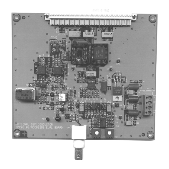
Page 6: Functional Description
Resistors R15, R15A, R16 and R18 provide the needed jumper J4. A standard ECL-level 100 MHz crystal input bias to the ADC08100. You can center the input oscillator should be installed at Y1 and the divide by 2 signal to the ADC by adjusting reference voltages V RT function selected by shorting pins 1 and 2 of jumper JP4. -
Page 7: Digital Data Output
4.4 Digital Data Output. simple to use, and to provide a quick and simple way to The digital output data from the ADC08100 is available at evaluate the ADC08100. The procedures given here will the 96-pin Euro connector J3. The series resistors of RP1 help you to properly set up the board. -
Page 8: Quick Check Of Software And Computer Interface Operation
, P, A or -X. Data transfer and CTRL the ADC08100 evaluation board. Note that which pins of calculations can take a few seconds. J5 are shorted (or whether any are shorted) is a "don't When transfer is complete, the data window should care"... -
Page 9: Troubleshooting
Section 4.6) and try again. - 5.2V.0 ±0.1V @ 250 mA Clock Frequency Range: 40 MHz to 250 MHz If there is no output from the ADC08100, perform the (divided by 2 for the ADC) following: Analog Input • Be sure that the proper voltages and polarities are Nominal Voltage: 1.6V P-P... -
Page 10: Hardware Schematic
+5VA 100pF +5VA ADC08100 CY7C4281 CY7C4281 AGND ADC_CLK 1.8k AGND ADC0 ADC1 WEN1 WEN1 _______ 2N3904 ADC2 WCLK 100MHz WCLK 47uF AGND 100MHz ADC3 6.3V WEN2/LD WEN2/LD LM833N ADC4 Vin GND DR VD ADC5 AGND REN1 REN1 DR GND +5VA... - Page 11 λ RED LED short +5VA 2N3904 R26A used R41A used 4.7k ADC_CLK MC10H125FN 100MHz-2 [ NOT USED ] NTE65 NTE65 MC10H125FN 100MHz MC10H125FN 100MHz _______ 100MHz MC10H131FN MC10H125FN [ NOT USED ] 50MHz CLK SEL MC10H131FN Figure 2b. ADC 08100 Evaluation Board Clock source...
-
Page 12: Evaluation Board Bill Of Materials
8.0 ADC08100 Evaluation Board Bill of Materials Item Qty Reference Part Source 10pF Type 1206 C2, C3, C4, C5, C6, C7, C9, C10, C11, C12, C14, Type 1206 C15, C16, C17B, C17A, C18, C23, C24, C25, C26, C27, C28, C29, C30, C31... -
Page 13: Summary Tables Of Test Points And Connectors
APPENDIX Summary Tables of Test Points and Connectors Test Points on the ADC08100 Evaluation Board TP 1 Power Down Input. Pull high to power down the ADC08100 TP 2 ADC Top Reference Voltage TP 3 Ground TP 4 ADC Bottom Reference Voltage... - Page 14 J3 Connector - ADC Data Outputs - Connection to WaveVision Digital Interface Board Signal J2 pin number ADC output D0 ADC output D1 ADC output D2 ADC output D3 ADC output D4 ADC output D5 ADC output D6 ADC output D7 ADC output D8 not used ADC output D9...
- Page 15 [ Blank Page ] http://www.national.com...
- Page 16 THE UNUSED PRODUCT FOR A REFUND OF THE PURCHASE PRICE PAID, IF ANY. The ADC08100 Evaluation Board is intended for product evaluation purposes only and is not intended for resale to end consumers, is not authorized for such use and is not designed for compliance with European EMC Directive 89/336/EEC.
Need help?
Do you have a question about the ADC08100 and is the answer not in the manual?
Questions and answers