
Subscribe to Our Youtube Channel
Related Manuals for National Semiconductor ADC121S625B


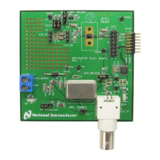
Summary of Contents for National Semiconductor ADC121S625B
- Page 1 July 25, 2006 National Semiconductor Rev - 2.1/CS RoHS Compliant Evaluation Board User's Guide ADC121S625 12-Bit, 50 kSPS to 200 kSPS, Differential Input, Micro-Power Sampling A/D Converter http://www.national.com...
-
Page 2: Table Of Contents
4.3 ADC Clock Circuit 4.4 Digital Data Output 4.5 Power Supply Connections 5.0 Software Operation and Settings 6.0 Hardware Schematic 7.0 Evaluation Board Specifications 8.0 ADC121S625B Evaluation Board Bill of Materials 9.0 Tables of Test Points, Jumpers and Connectors http://www.national.com... -
Page 3: Introduction
2.0 Board Assembly and evaluation is simplified by connecting this board to National Semiconductor's Data Capture The ADC121S625B evaluation board comes fully Board (order number WAVEVSN BRD 4.0) with a assembled and ready for use. Refer to the Bill of... -
Page 4: Quick Start
WV4ADCIFCABLE) between conversion process. ADC121S625B evaluation board and J3 of the WV4 board. 2. Connect a clean analog (non-switching) +5V power source to Power Connector J5. 5. Connect a clean analog (non-switching) +5V power source to Power Connector J5. -
Page 5: Functional Description
Board, voltage 5P0V for VA and 3P3V for U3 for the ADC121S625, apply the signal to be must be supplied to the ADC121S625B evaluation digitized across pins 1 & 3 of J3. Pin 2 of J3 is board. -
Page 6: Software Operation And Settings
The WaveVision4 software is included with the WV4 board and the latest version can be downloaded for free from National's web site at http://www.national.com/adc. install this software, follow the procedure in the WaveVision4 Board User's Guide. Once the software is installed, run it and set it up as follows: 1. -
Page 7: Hardware Schematic
6.0 Hardware Schematic Figure 2 ADC121S625B Evaluation Board Schematic http://www.national.com... -
Page 8: Evaluation Board Specifications
Power Requirements Min: +4.5V, Max: +5.5V, 100mA 100 mA Clock Frequency Range: 800 kHz to 4.0 MHz Analog Input 0V to 2VREF 8.0 ADC121S625B Evaluation Board Bill of Materials Item Reference Source Source Part # Value Footprint C1,C4,C5,C6,C10,C11,C14 sm/c_1206 Digikey 445-1423-2-ND 1.0uF... -
Page 9: Tables Of Test Points, Jumpers And Connectors
Terminal Block: Power connector for 5P0V. J6: CLK_IN BNC Connector: External clock input. Selection Jumpers on the ADC121S625B Evaluation Board (Refer to Table 1 in Section 4.0 for configuration details) JP1: VREF SELECT Selects reference source for VREF. JP2: VBIAS Provides DC bias for analog inputs. - Page 10 REFUND OF THE PURCHASE PRICE PAID, IF ANY. The ADC121S625B Evaluation Board is intended for product evaluation purposes only and is not intended for resale to end consumers, is not authorized for such use and is not designed for compliance with European EMC Directive 89/336/EEC, or for compliance with any other electromagnetic compatibility requirements.
Need help?
Do you have a question about the ADC121S625B and is the answer not in the manual?
Questions and answers