Table of Contents
Advertisement
Quick Links
This is the user's guide for the ADS42B4x EVM (Revision A). The ADS42B49 (dual-channel, 14-bit, up to
250 MSPS) is a dual analog-to-digital converter family. This EVM is specifically suited for interfacing with
TI's TSW1400 EVM to capture and display waveforms from the ADC. The EVM schematic, Bill of
Materials (BOM), and layout files are found in the design package in the ADS42B4x EVM product folder
on www.ti.com.
1
2
3
1
2
3
4
5
6
7
1
Default ADS42Bxx EVM Revision A Jumper Setting for Serial Interface
2
Parallel Interface with Pin Control of ADS58C28 and ADS42Bxx EVM Revision B Jumper Setting
3
4
5
Jumper and Component Settings for DDR LVDS Output and Parallel CMOS Output
SLAU477A - December 2012 - Revised January 2015
Submit Documentation Feedback
.............................................................................................................
.......................................................................................................
....................................................................................................
...............................................................................
............................................................................................
................................................................................................
...........................................................................................
...............................................................................................................
Copyright © 2012-2015, Texas Instruments Incorporated
SLAU477A - December 2012 - Revised January 2015
Contents
List of Figures
...............................................................
...............................................................
List of Tables
............................................
......................................................
....................................................
User's Guide
ADS42B4x EVM
.............
............................
ADS42B4x EVM
2
4
10
3
4
5
7
8
9
9
5
6
10
11
11
1
Advertisement
Table of Contents

Subscribe to Our Youtube Channel
Related Manuals for National Semiconductor ADS42B4 Series


Summary of Contents for National Semiconductor ADS42B4 Series
-
Page 1: Table Of Contents
User's Guide SLAU477A – December 2012 – Revised January 2015 ADS42B4x EVM This is the user’s guide for the ADS42B4x EVM (Revision A). The ADS42B49 (dual-channel, 14-bit, up to 250 MSPS) is a dual analog-to-digital converter family. This EVM is specifically suited for interfacing with TI’s TSW1400 EVM to capture and display waveforms from the ADC. -
Page 2: Software Control
Software Control www.ti.com Software Control Installation Instructions • Open folder named: ADS42Bxx_Installer_vxpx (where xpx represents the latest version) • Double-click: setup.exe • Follow on-screen instructions to complete GUI installation – Wait for ADS42Bxx_Installer initializing screen to complete – Click Next to install files in the default destination directory –... -
Page 3: Ads42Bxx_Gui Front Panel - Top Level
Software Control www.ti.com ● Low Speed Mode ChB: Low-speed mode for channel B ● LVDS Data Strength: Set the data strength from this switch ● LVDS Clkout Strength: Set the output clock strength from this switch ● CMOS Clk Strength: Set CMOS output clock strength from this switch ●... -
Page 4: Basic Test Procedure
Basic Test Procedure www.ti.com 1.2.3 Miscellaneous Settings ● Reset USB: Toggle this button if the USB port is not responding. This generates a new USB handle address. After hitting this, USB Status has to be turned to “Green”. ● Exit: Stops the program Basic Test Procedure This section outlines the basic test procedure for testing the EVM. -
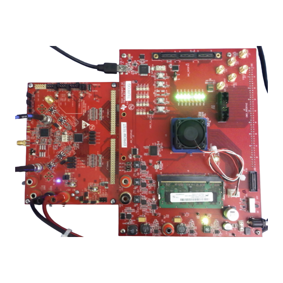
Page 5: Test Set-Up Block Diagram
Basic Test Procedure www.ti.com Test Block Diagram The test set-up for general testing of the ADS42B4x EVM with the TSW1400 capture card is shown in Figure Mini-USB Mini-USB Ref_out Signal Generator 15dBm TSW1400 ADS42B49EVM RX IF Signal J3/J6 Generator Ref_in ±1dBFS Figure 3. - Page 6 Basic Test Procedure www.ti.com Table 1. Default ADS42Bxx EVM Revision A Jumper Setting for Serial Interface (continued) Jumper Default position Function JP14 Short 7 - 8 ADC 2’s complement, DDR LVDS Short 1 - 2 ADC CTRL3, normal operation Short 1 - 2 ADC CTRL2, normal operation Short 1 - 2 ADC CTRL1, normal operation...
-
Page 7: High Speed Data Converter Pro
Basic Test Procedure www.ti.com TSW1400 Quick Start Operation Reference the TSW1400 User’s Guide for more detailed explanation of the TSW1400 set-up and operation. This document assumes that High Speed Data Converter Pro (HSDCPro) is installed and functioning properly. The front panel of HSDCPro is shown in Figure 4. -
Page 8: Ads42Bxx Gui
Basic Test Procedure www.ti.com ADS42B4x Test Procedure • Switch on the 5-V power supply for the EVM. • Connect clock signal at J19 through an appropriate bandpass filter. – Set the signal generator to 10 dBm and 250 MHz. – Use a high-quality, low phase-noise generator for this input to ensure proper device evaluation. –... -
Page 9: Fft Plot: 250-Mhz Clock, 170-Mhz Input To Channel A
Basic Test Procedure www.ti.com ADS42B4x Performance Results Figure 6 shows the performance result at 250-MSPS clock frequency and with a 170-MHz input tone. Figure 6 shows the performance of channel A from ADS42B4xEVM. SNR is 69.85 dBFS and SFDR is 82.85 dBFS. -
Page 10: Jumper Setting For Transformer-Coupled Or Opa-Driven Input
Optional Configurations www.ti.com Optional Configurations THS4509 Input Op-Amp Configuration The default analog input configuration is transformer coupling through T1 and T2 for channel A, and T3 and T4 for channel B. The optional configuration for analog input is through an Op-Amp THS4509. The changes required to modify the transformer coupled input to the OPA-driven input are shown in Table Table 3. -
Page 11: Optional Configurations
Optional Configurations www.ti.com On-Board CDCE72010 Clock The default clock input configuration is 1:4 transformer coupling through T6. The optional configuration is through clock driver CDCE72010. The changes required to modify the transformer coupled clock input to clock driver input are shown in Table Table 4. - Page 12 Revision History www.ti.com Revision History Changes from Original (December 2012) to A Revision ....................Page .................. • Changed register information in Top Level section................• Changed ADS42Bxx_GUI Front Panel – Top Level image.................. • Changed content in Miscellaneous Settings section..
- Page 13 STANDARD TERMS AND CONDITIONS FOR EVALUATION MODULES Delivery: TI delivers TI evaluation boards, kits, or modules, including any accompanying demonstration software, components, or documentation (collectively, an “EVM” or “EVMs”) to the User (“User”) in accordance with the terms and conditions set forth herein. Acceptance of the EVM is expressly subject to the following terms and conditions.
- Page 14 FCC Interference Statement for Class B EVM devices NOTE: This equipment has been tested and found to comply with the limits for a Class B digital device, pursuant to part 15 of the FCC Rules. These limits are designed to provide reasonable protection against harmful interference in a residential installation.
- Page 15 【無線電波を送信する製品の開発キットをお使いになる際の注意事項】 本開発キットは技術基準適合証明を受けておりません。 本製品のご使用に際しては、電波法遵守のため、以下のいずれかの措置を取っていただく必要がありますのでご注意ください。 1. 電波法施行規則第6条第1項第1号に基づく平成18年3月28日総務省告示第173号で定められた電波暗室等の試験設備でご使用 いただく。 2. 実験局の免許を取得後ご使用いただく。 3. 技術基準適合証明を取得後ご使用いただく。 なお、本製品は、上記の「ご使用にあたっての注意」を譲渡先、移転先に通知しない限り、譲渡、移転できないものとします。 上記を遵守頂けない場合は、電波法の罰則が適用される可能性があることをご留意ください。 日本テキサス・インスツルメンツ株式会社 東京都新宿区西新宿6丁目24番1号 西新宿三井ビル 3.3.3 Notice for EVMs for Power Line Communication: Please see http://www.tij.co.jp/lsds/ti_ja/general/eStore/notice_02.page 電力線搬送波通信についての開発キットをお使いになる際の注意事項については、次のところをご覧くださ い。http://www.tij.co.jp/lsds/ti_ja/general/eStore/notice_02.page SPACER EVM Use Restrictions and Warnings: 4.1 EVMS ARE NOT FOR USE IN FUNCTIONAL SAFETY AND/OR SAFETY CRITICAL EVALUATIONS, INCLUDING BUT NOT LIMITED TO EVALUATIONS OF LIFE SUPPORT APPLICATIONS.
- Page 16 SPACER Disclaimers: 6.1 EXCEPT AS SET FORTH ABOVE, EVMS AND ANY WRITTEN DESIGN MATERIALS PROVIDED WITH THE EVM (AND THE DESIGN OF THE EVM ITSELF) ARE PROVIDED "AS IS" AND "WITH ALL FAULTS." TI DISCLAIMS ALL OTHER WARRANTIES, EXPRESS OR IMPLIED, REGARDING SUCH ITEMS, INCLUDING BUT NOT LIMITED TO ANY IMPLIED WARRANTIES OF MERCHANTABILITY OR FITNESS FOR A PARTICULAR PURPOSE OR NON-INFRINGEMENT OF ANY THIRD PARTY PATENTS, COPYRIGHTS, TRADE SECRETS OR OTHER INTELLECTUAL PROPERTY RIGHTS.
- Page 17 IMPORTANT NOTICE Texas Instruments Incorporated and its subsidiaries (TI) reserve the right to make corrections, enhancements, improvements and other changes to its semiconductor products and services per JESD46, latest issue, and to discontinue any product or service per JESD48, latest issue.
Need help?
Do you have a question about the ADS42B4 Series and is the answer not in the manual?
Questions and answers