Table of Contents
Advertisement
Quick Links
National Semiconductor
Evaluation Board User's Guide
2
I
Analog-to-Digital Converter (ADC) with Alert Function
ALERT Option
ADDRESS Option
NOTE: The Evaluation Board is shipped with the Alert Option of the ADC. To
evaluate the Address Option, please order samples from www.national.com.
C-Compatible, 12-Bit, 10-Bit, or 8-Bit
12-bit
ADC121C021
ADC121C027
10-bit
ADC101C021
ADC101C027
January 3, 2008
Rev – 1.1/CC
RoHS Compliant
8-bit
ADC081C021
ADC081C027
Advertisement
Table of Contents

Related Manuals for National Semiconductor ADC121C021


Summary of Contents for National Semiconductor ADC121C021
- Page 1 January 3, 2008 National Semiconductor Rev – 1.1/CC RoHS Compliant Evaluation Board User's Guide C-Compatible, 12-Bit, 10-Bit, or 8-Bit Analog-to-Digital Converter (ADC) with Alert Function 12-bit 10-bit 8-bit ADC121C021 ADC101C021 ADC081C021 ALERT Option ADC121C027 ADC101C027 ADC081C027 ADDRESS Option NOTE: The Evaluation Board is shipped with the Alert Option of the ADC. To...
-
Page 2: Table Of Contents
Table of Contents 1.0 Introduction ..........................3 2.0 Board Assembly ........................4 3.0 Quick Start ..........................5 3.1 Stand Alone Mode.....................5 3.2 Computer Mode ......................5 4.0 Functional Description......................6 4.1 Jumper Settings ......................6 4.2 Analog Input Signal ....................7 4.3 ADC Reference Circuitry...................7 4.4 I C Interface ......................7 4.5 Alert Function ......................7 4.6 Automatic Conversion Mode ..................8... -
Page 3: Introduction
WV4 ADC081C021, and ADC081C027) will be referred Evaluation System. to as the ADC121C021 in this document. The ADCXX1C021 options offer an ALERT output pin, The WaveVision 4 software operates under whereas, the ADCXX1C027 offers an address Microsoft Windows. -
Page 4: Board Assembly
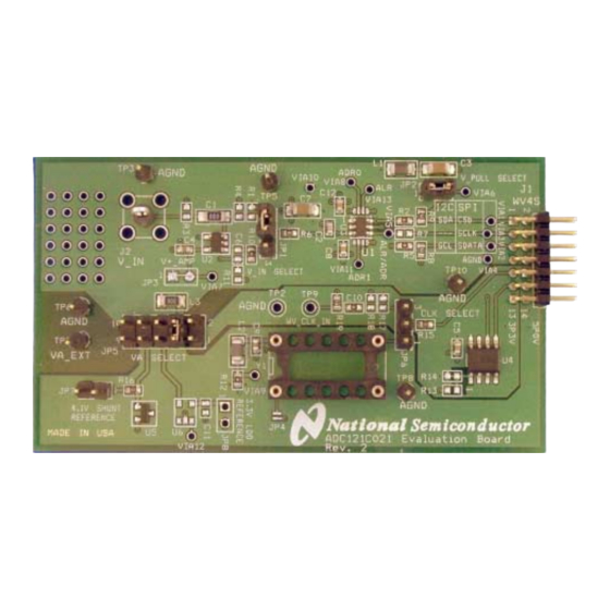
If needed, the input can be terminated by adding 2.0 Board Assembly an appropriate termination resistor at R3. The The ADC121C02XEB evaluation board comes V_IN footprint (J2) has been stuffed with a single- fully assembled and ready for use. The provided pin header for testing typical, slow-moving DC jumpers are in their recommended locations and input signals. -
Page 5: Quick Start
3.0 Quick Start address to 52hex. The ADC121C02XEB evaluation board may be 8. If evaluating the ADC121C021, the slave used in the Stand Alone mode to capture data address is permanently set to 54hex. with a logic analyzer or third party equipment, or it 9. -
Page 6: Functional Description
4. Connect the J1 header on the ADC121C021 7. Refer to Section 5.0 on Software Operation evaluation board to the WV4 serial connector and Settings to setup the WaveVision 4 (J7) on the WV4 board. Refer to Figure 6 for software. -
Page 7: Analog Input Signal
2 of JP1. The signal’s return 4.4 I C Interface (GND) should be connected to TP5. This Please refer to section 1.7 of the ADC121C021 configuration provides the input circuit seen in datasheet for a detailed description of the I Figure 8. interface. -
Page 8: Automatic Conversion Mode
• For V = +5.0V, I = 11mA Note: A majority of this current is for powering devices external to the ADC121C021 such as the pull-up resistors and the input amplifier. When operating in the computer mode, the supply voltage for V can be applied externally or supplied directly by the WV4 board through J1. -
Page 9: Data Analysis
4. Click on the "Close" button to close the changed to reflect the state of the address System Settings window. selection pin (ADDR). 5. Navigate to the ADC121C021 Eval Board 8. Press the “Read Registers” button. All of the Window. This is the Control Panel for the register fields will update (Figure 10). -
Page 10: Register Control
Enter. All hex values are assumed to be right justified. Zeros are written to unspecified bits. Many functions of the ADC121C021 are enabled through the internal registers. Please refer to Section 1.6 on Internal Registers in the Datasheet for further details. -
Page 11: Troubleshooting Wavevision
WaveVision. If evaluating the Problem 3: The following error occurs when I try ADC121C021, the address must be set to 0x54. to read or write registers through the Control If evaluating the ADC121C027, the address will Panel. Try Solution D. -
Page 12: Evaluation Board Specifications
14 pin dual row right angle male header: Connects to WV4 board. J2: V_IN Analog Input of the Eval Board. Selection Jumpers on the ADC121C021 Evaluation Board (Refer to table 1 in Section 4.0 for configuration details) JP1: V_IN SELECT Selects buffered or unbuffered signal path. -
Page 13: Hardware Schematic
8.0 Hardware Schematic Figure 10: ADC121C021 Evaluation Board Schematic http://www.national.com... -
Page 14: Evaluation Board Layers
9.0 Evaluation Board Layers Figure 11: ADC121C021 Evaluation Board: All Layers with Silk Screen Figure 12: ADC121C021 Evaluation Board: Top Layer Figure 13: ADC121C021 Evaluation Board: Bottom Layer http://www.national.com... -
Page 15: Evaluation Board Bill Of Materials
R10,R12 R8,R9 R15,R19 AGND TP3,TP6 AGND Digikey 5011K-ND TP5,TP8, AGND Digikey Single-pin TP10 Header VA_EXT Digikey 5011K-ND WV_CLK_IN ADC121C021 ADC -TSOT6 ADC121C021CIMK LMP7731 AMP-SOT23-5 LMP7731MF MSOP8 24C02 EEPROM LM4050-4.1 SHUNT REF LM4050AIM3-4.1 LDO-SOT23-5 LM4132AMF-3.3 VIA1-13 OSC (Socket) Digikey A400-ND Aries 08-3518-10 http://www.national.com... - Page 16 European EMC Directive 89/336/EEC, or for compliance with any other electromagnetic compatibility requirements. National Semiconductor Corporation does not assume any responsibility for use of any circuitry or software supplied or described. No circuit patent licenses are implied.
- Page 17 EVALUATION BOARD/KIT/MODULE (EVM) ADDITIONAL TERMS Texas Instruments (TI) provides the enclosed Evaluation Board/Kit/Module (EVM) under the following conditions: The user assumes all responsibility and liability for proper and safe handling of the goods. Further, the user indemnifies TI from all claims arising from the handling or use of the goods.
- Page 18 FCC Interference Statement for Class B EVM devices This equipment has been tested and found to comply with the limits for a Class B digital device, pursuant to part 15 of the FCC Rules. These limits are designed to provide reasonable protection against harmful interference in a residential installation. This equipment generates, uses and can radiate radio frequency energy and, if not installed and used in accordance with the instructions, may cause harmful interference to radio communications.
- Page 19 【 【 Important Notice for Users of this Product in Japan】 】 This development kit is NOT certified as Confirming to Technical Regulations of Radio Law of Japan If you use this product in Japan, you are required by Radio Law of Japan to follow the instructions below with respect to this product: 1.
- Page 20 EVALUATION BOARD/KIT/MODULE (EVM) WARNINGS, RESTRICTIONS AND DISCLAIMERS For Feasibility Evaluation Only, in Laboratory/Development Environments. Unless otherwise indicated, this EVM is not a finished electrical equipment and not intended for consumer use. It is intended solely for use for preliminary feasibility evaluation in laboratory/development environments by technically qualified electronics experts who are familiar with the dangers and application risks associated with handling electrical mechanical components, systems and subsystems.
-
Page 21: Important Notice
IMPORTANT NOTICE Texas Instruments Incorporated and its subsidiaries (TI) reserve the right to make corrections, enhancements, improvements and other changes to its semiconductor products and services per JESD46, latest issue, and to discontinue any product or service per JESD48, latest issue.
Need help?
Do you have a question about the ADC121C021 and is the answer not in the manual?
Questions and answers