Sony UWP-V1 Service Manual
Uhf wireless microphone package
Hide thumbs
Also See for UWP-V1:
- Operating instructions manual (72 pages) ,
- User manual (12 pages) ,
- Product manual (12 pages)
Table of Contents
Advertisement
Quick Links
Advertisement
Chapters
Table of Contents

Related Manuals for Sony UWP-V1


Summary of Contents for Sony UWP-V1
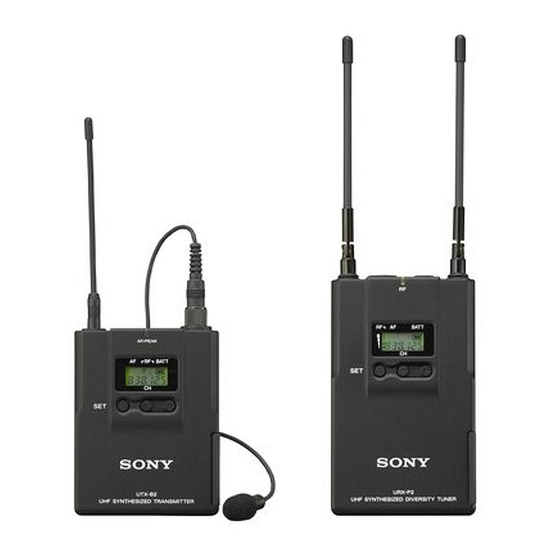
- Page 1 UHF WIRELESS MICROPHONE PACKAGE UWP-V1 UWP-V2 UWP-V6 UWP-X7 UWP-X8 UHF SYNTHESIZED TRANSMITTER UTX-B2 UHF SYNTHESIZED WIRELESS MICROPHONE UTX-H2 UHF SYNTHESIZED TUNER UNIT URX-M2 UHF SYNTHESIZED DIVERSITY TUNER URX-P2 UHF SYNTHESIZED TRANSMITTER UTX-P1 SERVICE MANUAL 1st Edition...
- Page 2 ! WARNING This manual is intended for qualified service personnel only. To reduce the risk of electric shock, fire or injury, do not perform any servicing other than that contained in the operating instructions unless you are qualified to do so. Refer all servicing to qualified service personnel.
-
Page 3: Table Of Contents
3-3-5. UTX-P1 ............... 3-36 1-3-3. Error Messages ............ 1-10 3-4. Accessories Supplied ............ 3-40 1-4. URX-P2 ................ 1-11 3-4-1. UWP-V1 .............. 3-40 1-4-1. Disassembly ............1-11 3-4-2. UWP-V2 .............. 3-40 1-4-2. Precaution for Reassembling ....... 1-12 3-4-3. UWP-V6 .............. 3-41 3-4-4. -
Page 5: Service Overview
Section 1 Service Overview 1-1. UTX-B2 1-1-1. Disassembly Rear cabinet (TX) Antenna/CPU-422 board M2 x 10 M2 x 10 CN401 M2 x 10 M2 x 10 CPU422 board P2 x 5 Antenna Rear cabinet (TX) Mic sheet Battery case assembly Be careful not to drop or lose this. -
Page 6: Precaution For Reassembling
1-1-2. Precaution for Reassembling When reassembling the UTX-B2, arrange the battery harnesses as shown in the following figures. Battery spring (Black) (Red) Harness Battery spring plate Arranging the harnesses as shown in the figures. Front side Rear side Front cabinet Tape for insulation Note When reassembling the UTX-B2, be careful that... -
Page 7: Precaution When Replacing Eeprom (Ic611)
1-1-3. Precaution When Replacing EEPROM (IC611) When the EEPROM (IC611) is replaced with the new EEPROM, the same data that have been stored in the removed EEPROM must be written into the newly mounted EEPROM. 1-1-4. Error Messages When an error occurs, any of the following error messages can be generated by the self-diagnostics function that is built-in the UTX-B2 and can appear on the display section. -
Page 8: Utx-H2
1-2. UTX-H2 1-2-1. Disassembly Cage sub assembly Grip (B) Grip (B) *Grip removal fixture Model cover Grip (B) Cage sub assembly Ring stopper Push up the claws. *Grip removal fixture (If difficult to remove, Dynamic unit unlock one claw after another.) Do not touch the portion * : Tools required :... - Page 9 Grip (A) Antenna/MB-1137 board Indicator Precision P2.6 x 5 Power button Power lock Stopper Antenna Stopper Chassis (B) sub Disengage the claw of assembly the chassis (A) using a flat head (_) screwdriver, and remove the stopper. Claw of the chassis (A) Chassis (A) assembly Precision...
-
Page 10: Precaution When Replacing Eeprom (Ic401)
1-2-2. Precaution When Replacing EEPROM (IC401) When the EEPROM (IC401) is replaced with the new EEPROM, the same data that have been stored in the removed EEPROM must be written into the newly mounted EEPROM. 1-2-3. Error Messages When an error occurs, any of the following error messages can be generated by the self-diagnostics function that is built-in the UTX-H2 and can appear on the display section. -
Page 11: Urx-M2
1-3. URX-M2 1. Tuner Base Unit MB-X6 / MB-806A 1-3-1. Removal/Installation When using the MB-X6 Removal . Before installing the URX-M2, make sure the MB-806A 1. Loosen the screws at both sides of the front cover, then into which the URX-M2 will be installed is turned off. Do slide the front cover downward. - Page 12 Installation When using the MB-806A Removal 1. After removing the front cover, hold the tuner unit by the top and bottom, then insert the tuner unit into the 1. On the bottom panel of the MB-806A, locate the lever slot. corresponding to the slot of the URX-M2 to be removed and pull the lever forward.
- Page 13 2. Powered Mixer SRP-X500P / SRP-X700P When using the SRP-X700P Removal When using the SRP-X500P 1. Insert a screwdriver into the hole under the lower part Removal of the tuner slot and remove the URX-M2. 1. Pull the latch securing the tuner unit to the side and Screwdriver : Shaft diamter is between 2 to 4 mm pull out the tuner unit URX-M2.
-
Page 14: Urx-M2 Checking
1-3-2. URX-M2 Checking The following procedures describe how to prove URX-M2 whether it needs to be required or not. Equipment Required : MB-X6 (quality unit) / MB-806A (quality unit) URX-M2 (quality unit) 1. Install the URX-M2 (repair unit) to be checked in an MB-X6 / MB-806A (quality unit). 2. -
Page 15: Urx-P2
1-4. URX-P2 1-4-1. Disassembly Rear cabinet Antenna/RF-130 board M2 x 10 RF-130 board M2 x 10 Antenna Rear cabinet (RX) Battery case assembly Stereo miniature jack CPU-421 board Supplied washer Battery spring Supplied nut plate CPU-421 board Stereo P2 x 5 miniature jack P2 x 5 P2 x 5... -
Page 16: Precaution For Reassembling
1-4-2. Precaution for Reassembling When reassembling the UTX-P2, arrange the battery harnesses as shown in the following figures. Battery spring (Black) (Red) Harness Battery spring plate Arranging the harnesses as shown in the figures. Front side Rear side Front cabinet Tape for insulation Note When reassembling the UTX-B2, be careful that... -
Page 17: Precaution When Replacing Eeprom (Ic11)
1-4-3. Precaution When Replacing EEPROM (IC11) When the EEPROM (IC11) is replaced with the new EEPROM, the same data that have been stored in the removed EEPROM must be written into the newly mounted EEPROM. 1-4-4. Error Messages When an error occurs, any of the following error messages can be generated by the self-diagnostics function that is built-in the URX-P2 and can appear on the display section. -
Page 18: Utx-P1
1-5. UTX-P1 1-5-1. Disassembly Upper sub assembly Four screws P2 x 6 Upper sub assembly Notch Battery case Battery case Four screws P2 x 6 Press and hold the notch, and pull up the upper sub assembly. Case XLA connector Coil spring XLA connector Case... -
Page 19: Precaution For Reassembling
1-5-2. Precaution for Reassembling When reassembling the UTX-P1, be sure that the knob on the case and the switch on the MB-1094 board fit together correctly. Case Knob Knob Panel Lever Switch MB-1094 board 1-6. Unleaded Solder Boards requiring use of unleaded solder are printed with a lead free mark (LF) indicating the solder contains no lead. -
Page 21: Electrical Alignment
Section 2 Electrical Alignment 2-1. UTX-B2 2-1-1. Equipment and Tools Equipment Required Name Specifications Model Name DC POWER SUPPLY Output regulated voltage : 0 to 5 V, 2 A – DC AMMETER Measurement : 300 mA – SPECTRUM ANALYZER Frequency : 10 kHz to 3 GHz ADVANTEST R3361B or equivalent MODULATION ANALYZER RF input Frequency : 150 kHz to 3 GHz... -
Page 22: Adjustments
2-1-2. Adjustments 3. Connecting the DC power supply Supply the DC power to the battery terminal as below. This section describes adjustments and checks which must be completed to assure that the specifications are complied with. Make adjustment and checks following the procedure below: POWER 1. -
Page 23: Equipment And Tools
Adjustment Location Connections (For connecting the DC power supply, refer to step “3. Connecting the DC power supply” in Section 2-1-2.) CT621 C24 (+) CPU-422 board (B side) S673 S672 S671 CPU-422 board (B side) CN301 RV521 (Reference frequency RV351 deviation adjustment) DC voltmeter (RF output "H"... - Page 24 . Frequency counter Specification : Carrier frequency mentioned below. U30 model ; 578.125 MHz ± 1 kHz . Adjustor (SONY Part No. 7-721-052-81) U42 model ; 650.125 MHz ± 1 kHz . MM-SMA conversion connector CE62 model ; 810.000 MHz ± 1 kHz (SONY Part No.
- Page 25 2. Adjust 1CT361 so that the power meter reading meets . Power meter (with power sensor) the following specification. . Adjustor (SONY Part No. 7-721-052-81) Specification : power meter = Maximum . MM-SMA conversion connector Adjustment : 1CT361/RF-131 board (A side) (SONY Part No.
- Page 26 DE EMPHASIS connector change switch Modulation Oscilloscope analyzer (S401 / RF-131 board) . Adjustor (SONY part No. 7-721-052-81) . MM-SMA conversion connector (SONY Part No. J-6402-490-A) CN301 . SMA-BNC conversion connector (SONY Part No. J-6402-480-A) Switch and Control Setting Transmission channel U30 model ;...
- Page 27 : 15 kHz or 20 kHz DC output voltage : +3.0 ± 0.1Vdc DE EMPHASIS : 50 usec . Oscilloscope . DC current meter . Adjustor (SONY part No. 7-721-052-81) . Audio analyzer . MM-SMA conversion connector . Modulation analyzer (SONY Part No. J-6402-490-A) MEASUREMENT : FM MEASUREMENT RANGE : AUTO or ±...
- Page 28 DE EMPHASIS : 50 usec . Oscilloscope MM-SMA conversion connector and SMA-BNC conversion connector . MM-SMA conversion connector Distortion analyzer (SONY Part No. J-6402-490-A) . SMA-BNC conversion connector AF input MIC / LINE (SONY Part No. J-6402-480-A) connector change switch Modulation...
- Page 29 (SONY Part No. J-6402-480-A) . Frequency counter . Spectrum analyzer Switch and Control Setting . Modulation analyzer . RF adjusting cable (SONY part No. 7-721-052-81) Transmission channel . MM-SMA conversion connector U30 model ; 32-01 channel (578.125 MHz) U42 model ;...
- Page 30 Frequency deviation adjustment Frequency check Connections Connections (For connecting the DC power supply, refer to step (For connecting the DC power supply, refer to step “3. Connecting the DC power supply” in Section 2-1-2.) “3. Connecting the DC power supply” in Section 2-1-2.) Modulation MM-SMA conversion connector and analyzer...
- Page 31 Shorted between GND and AF IN (HOT) . DC ammeter Solder Lead wire . Spectrum analyzer CL402 . MM-SMA conversion connector (SONY Part No. J-6402-490-A) . SMA-BNC conversion connector Solder (SONY Part No. J-6402-480-A) Switch and Control Setting Spectrum analyzer Transmission channel U30 model ;...
- Page 32 ; 746.125 MHz ± 1 kHz . Spectrum analyzer KR model . MM-SMA conversion connector REFERENCE LEVEL : 20 dBm (10 dBm ; (SONY Part No. J-6402-490-A) KR model only) . SMA-BNC conversion connector FREQUENCY SPAN : 500kHz (50 kHz/DIV) (SONY Part No. J-6402-480-A)
- Page 33 2-2. UTX-H2 2-2-1. Equipment and Tools Equipment Required Name Specifications Model Name DC POWER SUPPLY Output regulated voltage : 0 to 5 V, 2 A – DC AMMETER Measurement : 300 mA – SPECTRUM ANALYZER Frequency : 10 kHz to 3 GHz ADVANTEST R3361B or equivalent MODULATION ANALYZER RF input Frequency : 150 kHz to 3 GHz...
-
Page 34: Adjustments
2-2-2. Adjustments 3. Connecting the DC power supply Supply the DC power to the battery terminal on MB- This section describes adjustments and checks which must be 1137 board using the wires as below. completed to assure that the specifications are complied with. Solder here. - Page 35 1. Power Supply Voltage Check Adjustment Location Equipment and Tools . DC power supply DC output voltage : +3.0 ± 0.1 Vdc CT101 . DC ammeter (Transmitter output) RV102 RV104 . Digital volt meter (or Digital multimeter) (Transmitter output : H) (Transmitter output : L) RV101 Switch and Control Setting...
- Page 36 . DC ammeter meets the following specification. . Frequency counter Specification : Carrier frequency mentioned below. ; 578.125 MHz ± 1 kHz . Adjustor (SONY Part No. 7-721-052-81) U30 model ; 650.125 MHz ± 1 kHz . MM-SMA conversion connector U42 model CE62 model ;...
- Page 37 . DC ammeter the following specification. . Power meter (with power sensor) Specification : power meter = Maximum . Adjustor (SONY Part No. 7-721-052-81) Adjustment : 1CT101/MB-1137 board (A side) . MM-SMA conversion connector (Refer to page 2-16 for the adjustment location.) (SONY Part No.
- Page 38 : 20 kHz or 15 kHz MM-SMA conversion connector and : 50 usec DE EMPHASIS CN101 SMA-BNC conversion connector . Adjustor (SONY part No. 7-721-052-81) . MM-SMA conversion connector Audio analyzer Level meter (SONY Part No. J-6402-490-A) Oscillator . SMA-BNC conversion connector (SONY Part No.
- Page 39 : 15 kHz or 20 kHz DE EMPHASIS : 50 usec . DC ammeter . Oscilloscope . Audio analyzer . Adjustor (SONY part No. 7-721-052-81) . Modulation analyzer . MM-SMA conversion connector MEASUREMENT : FM MEASUREMENT RANGE : AUTO or ± 40 kHz (SONY Part No.
- Page 40 DE EMPHASIS : 50 usec Oscilloscope . Oscilloscope MM-SMA conversion connector . MM-SMA conversion connector SMA-BNC conversion connector (SONY Part No. J-6402-490-A) . SMA-BNC conversion connector (SONY Part No. J-6402-480-A) RF IN Distortion Switch and Control Setting analyzer MB-1137 board...
- Page 41 . DC ammeter . Frequency counter Switch and Control Setting . Spectrum analyzer . Modulation analyzer MB-1137 board . RF adjusting cable (SONY part No. 7-721-052-81) Transmission channel U30 model ; 32-01 channel (578.125 MHz) . MM-SMA conversion connector U42 model ;...
- Page 42 Frequency deviation adjustment Frequency check Connections Connections (For connecting the DC power supply, refer to step (For connecting the DC power supply, refer to step “3. Connecting the DC power supply” in Section 2-2-2.) “3. Connecting the DC power supply” in Section 2-2-2.) MB-1137 board (B side) Spectrum analyzer Modulation...
- Page 43 DC output voltage : +3.0 ± 0.1Vdc “4.Reference Frequency Deviation Adjustment”. . DC ammeter . Spectrum analyzer . MM-SMA conversion connector Spectrum analyzer (SONY Part No. J-6402-490-A) . SMA-BNC conversion connector (SONY Part No. J-6402-480-A) Switch and Control Setting MM-SMA conversion connector and MB-1137 board...
- Page 44 “4.Reference Frequency Deviation Adjustment”. . DC ammeter . Audio analyzer . Spectrum analyzer Spectrum analyzer . MM-SMA conversion connector (SONY Part No. J-6402-490-A) . SMA-BNC conversion connector (SONY Part No. J-6402-480-A) MM-SMA conversion connector and SMA-BNC conversion connector Switch and Control Setting...
- Page 45 Procedure 1. Set the spectrum analyzer as below: CENTER FREQUENCY : U30 model ; 578.125 MHz ± 1 kHz U42 model ; 650.125 MHz ± 1 kHz CE62 model ; 810.000 MHz ± 1 kHz CE67 model ; 850.000 MHz ± 1 kHz ;...
- Page 46 Input impedance : 600 Z (balanced) (with A-weighted filter) Oscilloscope Frequency : DC to 30 MHz Tuner base unit Quality unit Sony MB-X6 or MB-806 Tools Name Part No. Remarks Adjuster (0.4 x 1.3 mm) 7-721-052-81 For adjustment DC cut fixture Refer to “How to make DC cut fixture”...
-
Page 47: Adjustments
2-3-2. Adjustments Calibration method 1. Connect the RF millivoltmeter to the signal generator as This section describes the following adjustments (and shown in the figure below. checks) required to satisfy the specifications. 2. Adjust the level of the output signal from the signal gen- erator (SSG) so that the RF millivoltmeter reads 50 mV. - Page 48 1. Current Consumption Check 2. Reference Frequency (4 MHz oscillation frequency) Adjustment Equipment and Tools . DC power supply Equipment and Tools DC output voltage : +9.0Vdc ± 0.1 V . DC power supply DC output voltage : +9.0Vdc ± 0.1 V .
- Page 49 3. Output Level Adjustment Switch and Control Setting . URX-M2 Front panel Perform this adjustment when the TUNER OUTPUT levels Channel setting : deviate from the specification. U30 model ; Group 03, 32-01 channel (578.125 MHz) U42 model ; Group 03, 44-01 channel (650.125 MHz) Preparation CE62 model ;...
- Page 50 4. RF Squelch Level/RF Indicator Level 5. Adjustment (ANTENNA B IN side adjustment) Adjustment Point : TUNER OUTPUT 1 Specification : Output level (level meter indication level) = _20 dBm ± 0.5 dB (at 600 Z Perform this adjustment when Muting levels deviate from loaded) the specification.
- Page 51 Procedure 7. When a message appears on the LCD (URX-M2), all segments light on. Then pressing the following buttons in the order starting from “SET” → “+” → “_” → Preparation “SET” buttons while all segments are lighting. 8. Indication on LCD (URX-M2, Tuner [1]) appears as Set the signal generator as follows : Signal generator setting follows :...
- Page 52 12. Set the FREQUENCY (carrier frequency) of the signal 20. Check first that indication “L” of “BC1L” on the LCD (URX-M2, Tuner [1]) has disappeared, and then press generator as follows : FREQUENCY (carrier frequency) : the “SET” button of the URX-M2. 21.
- Page 53 27. Indication on the LCD (URX-M2, Tuner [1]) appears 5. Overall Characteristics Check as follows : LCD : Perform the overall characteristics check according to the following procedure. Model LCD message Procedure (1) Output Level Check ↓ CE62 CE62 (2) S/N Check CE67 CE67 ↓...
- Page 54 (1) Output Level Check (2) S/N Check Procedure Procedure The checking procedures describe that the URX-M2 (to be The checking procedures describe that the URX-M2 (to be adjusted) is installed into the Tuner [1] slot on the MB-X6 or adjusted) is installed into the Tuner [1] slot on the MB-X6 or MB-806.
- Page 55 (3) Frequency Characteristic Check 9. Check that output level of the TUNER OUTPUT 1 is 36 dB or more (S/N is _36 dB or less with A-weighted fil- Procedure ter) as compared with the level of procedure 5 above. 10. Change the RF OUTPUT (output level) of the signal generator as shown below.
-
Page 56: Tuner Output 1
(4) Distortion Ratio Check 6. Change the MODULATION (modulation frequency) of the signal generator as follows, and check the output Procedure level of the OUTPUT connector is set also as follows. 40 Hz and 18 kHz modulation frequency must be set by using the function generator. - Page 57 (5) RF Squelch Level/RF Indicator Check 8. Connect the signal generator to the ANTENNA B IN connector with DC cut fixture. Procedure 9. Perform the procedures 3 to 7 above. 10. Set the channel and FREQUENCY (carrier frequency) of the signal generator as shown 1 and 2 below. The checking procedures describe that the URX-M2 (to be Perform the procedures 1 to 9 above, for each channel adjusted) is installed into the Tuner [1] slot on the MB-X6 or...
- Page 58 (6) RF Level Indicator Check 5. Connect the signal generator to the ANTENNA B IN connector with DC cut fixture. Procedure 6. Perform the procedures 3 to 4 above. 7. Set the channel setting (Tuner [1]) and FREQUENCY (carrier frequency) of the signal generator as shown 1 The checking procedures describe that the URX-M2 (to be and 2 below.
-
Page 59: Mb-X6
(7) AF Level Indicator/AF Indicator Check (8) Tone Squelch Check Procedure Procedure The checking procedures describe that the URX-M2 (to be The checking procedures describe that the URX-M2 (to be adjusted) is installed into the Tuner [1] slot on the MB-X6 or adjusted) is installed into the Tuner [1] slot on the MB-X6 or MB-806. - Page 60 Remarks MM-SMA conversion connector J-6402-490-A RF adjusting cable J-6402-390-A AF output cable 1-792-249-11 . Supplied accessory of UWP-V1, V2 . Wiring diagram 3-pole mini Phone plug (Ø3.5) XLR, 3P connector (male) Chip 1 ; GND 2 ; HOT 3 ; COLD —Wiring side—...
-
Page 61: Adjustments
2-4-2. Adjustments Calibration method 1. Connect the RF millivoltmeter to the signal generator as shown in the figure below. This section describes the following adjustments (and 2. Adjust the level of the output signal from the signal gen- checks) required to satisfy the specifications. erator (SSG) so that the RF millivoltmeter reads 50 mV. - Page 62 2. Connect the DC power supply (DC +3 V ±0.1 V) and 1. Current Consumption Check the DC ammeter as shown in the following figure. Equipment and Tools . DC power supply DC output voltage : +3.0Vdc ± 0.1 V .
- Page 63 2. Reference Frequency (4 MHz oscillation frequency) Adjustment CPU-421 board (B side) Equipment and Tools . DC power supply DC output voltage : +3.0Vdc ± 0.1 V . Frequency counter Switch and Control Setting Set the URX-P2 as follows : S681 Channel setting : "...
- Page 64 3. Output Level Adjustment Switch and Control Setting Set the URX-P2 as follows : Perform this adjustment when the TUNER OUTPUT levels Channel setting : deviate from the specification. U30 model ; Group 03, 3201 channel (578.125 MHz) U42 model ; Group 03, 4401 channel (650.125 MHz) Preparation CE62 model ;...
- Page 65 4. RF Squelch Level/RF Indicator Level 5. Adjustment (ANTENNA B side adjustment) Adjustment Point : OUTPUT Specification : Output level (level meter indication level) = _46 dBm ± 0.5 dB (at 600 Z Perform this adjustment when Muting levels deviate from loaded) the specification.
- Page 66 Adjustment If the LCD (on A area: refer to the previous proce- 1. Connect the signal generator to the CN201/RF-130 dure 7) displays below, perform the following adjust- board with the MM-SMA conversion connector and ment (1) or (2). the RF adjusting cable. .
-
Page 67: Adjustment Is Completed. (Normal Operation Mode)
14. Set the FREQUENCY (carrier frequency) of the signal 22. Check first that indication “L” of “BC2L” on the LCD generator as follows : (URX-P2) has disappeared, and then press the “SET” FREQUENCY (carrier frequency) : button of the URX-P2. U30 model ;... - Page 68 5. Overall Characteristics Check (1) Output Level Check Perform the overall characteristics check according to the 1. Set the URX-P2 as follows : following procedure. Channel setting : U30 model ;Group 03, 3201 channel (578.125 MHz) Procedure U42 model ;Group 03, 4401 channel (650.125 MHz) (1) Output Level Check CE62 model ;Group 04, 6332 channel (810.000 MHz) (2) S/N Check...
- Page 69 (2) S/N Check 13. Connect the signal generator to the CN101/RF-130 board with the MM-SMA conversion connector and the 1. Set the URX-P2 as follows : RF adjusting cable. Channel setting : 14. Perform the procedures 4 to 12 above. U30 model ;Group 03, 3201 channel (578.125 MHz) 15.
- Page 70 Procedure Notes 1. Reassembly URX-P2 completely. Because the audio system of the URX-P2 is output in the 2. Turn on the power of the URX-P2 following the unbalanced system, the noise level can be possibly so high procedure. (For setting, refer to “Setting the Squelch that the S/N measurement becomes impossible depending OFF mode”...
- Page 71 (3) Frequency Characteristic Check (4) Distortion Ratio Check 1. Set the URX-P2 as follows : 1. Set the URX-P2 as follows : Channel setting : Channel setting : U30 model ;Group 03, 3201 channel (578.125 MHz) U30 model ;Group 03, 3201 channel (578.125 MHz) U42 model ;Group 03, 4401 channel (650.125 MHz) U42 model ;Group 03, 4401 channel (650.125 MHz) CE62 model ;Group 04, 6332 channel (810.000 MHz)
- Page 72 (5) RF Squelch Level/RF Indicator Check 10. Set the channel and FREQUENCY (carrier frequency) of the signal generator as shown 1 and 2 below. 1. Set the URX-P2 as follows : Perform the procedures 1 to 9 above, for each channel setting (1 and 2).
- Page 73 (6) RF Level Indicator Check 5. Connect the signal generator to the CN101/RF-130 board with the MM-SMA conversion connector and the 1. Set the URX-P2 as follows : RF adjusting cable. Channel setting : 6. Perform the procedures 3 to 4 above. U30 model ;Group 03, 3201 channel 7.
- Page 74 (8) Tone Squelch Check (7) AF Level Indicator/AF Indicator Check 1. Set the URX-P2 as follows : 1. Set the URX-P2 as follows : URX-P2 Front panel Channel setting : Channel setting : U30 model ;Group 03, 3201 channel (578.125 MHz) U30 model ;...
- Page 75 Level meter Equipment . Stereo mini-plug with cable (diameter : 3.5 mm) (Sony RK-G136 (accessory), or equivalent) : 1 . Resister, carbon 16Z 1/4W (Part No. 1-247-088-00) : 2 Stereo mini-plug To use the cable RK-G136, cut it into an appropriate...
- Page 76 2-5. UTX-P1 2-5-1. Equipment and Tools Equipment Required Name Specifications Model Name DC POWER SUPPLY Output regulated voltage : 0 to 5 V, 2 A – DC AMMETER Measurement : 300 mA – SPECTRUM ANALYZER Frequency : 10 kHz to 3 GHz ADVANTEST R3361B or equivalent MODULATION ANALYZER RF input Frequency : 150 kHz to 3 GHz...
-
Page 77: Adjustments
2-5-2. Adjustments 3. Connecting the DC power supply Supply the DC power to the battery terminal on MB- This section describes adjustments and checks which must be 1094 board using the wires as below. completed to assure that the specifications are complied with. DC regulated power supply Make adjustment and checks following the procedure below: (DC output voltage : + 3.0 ±0.1 V) - Page 78 1. Power Supply Voltage Check Adjustment Location Equipment and Tools . DC power supply LINE DC output voltage : +3.0 ± 0.1 Vdc . DC ammeter . Digital volt meter (or Digital multimeter) Switch and Control Setting MB-1094 board CT401 Transmission channel (Transmitter frequency) U30 model...
- Page 79 . DC ammeter meets the following specification. . Frequency counter Specification : Carrier frequency mentioned below. 578.125 MHz ± 1 kHz . Adjustor (SONY Part No. 7-721-052-81) U30 model ; 650.125 MHz ± 1 kHz . MM-SMA conversion connector U42 model ;...
- Page 80 2. Adjust 1RV102 so that the power meter reading meets . DC ammeter the following specification. . Power meter (with power sensor) Specification : . Adjustor (SONY Part No. 7-721-052-81) . U30 model : . MM-SMA conversion connector Power meter = 18 mW (SONY Part No. J-6402-490-A) .
- Page 81 MEASUREMENT RANGE : AUTO or ± 40 kHz : 50 Hz : 20 kHz or 15 kHz : 50 usec DE EMPHASIS . Adjustor (SONY part No. 7-721-052-81) . MM-SMA conversion connector (SONY Part No. J-6402-490-A) . SMA-BNC conversion connector MB-1094 board (SONY Part No.
- Page 82 : 15 kHz or 20 kHz 6. Distortion Ratio Check : 50 usec DE EMPHASIS . Oscilloscope . Adjustor (SONY part No. 7-721-052-81) Equipment and Tools . MM-SMA conversion connector . DC power supply DC output voltage : +3.0 ± 0.1Vdc (SONY Part No.
- Page 83 : 15 kHz or 20 kHz DE EMPHASIS : 50 usec RF IN Distortion . Oscilloscope analyzer SMA-BNC . MM-SMA conversion connector conversion (SONY Part No. J-6402-490-A) Modulation connector Oscillator analyzer . SMA-BNC conversion connector MM-SMA (SONY Part No. J-6402-480-A) conversion connector...
- Page 84 . DC current meter . Frequency counter Switch and Control Setting . Spectrum analyzer . Modulation analyzer MB-1094 board . RF adjusting cable (SONY part No. 7-721-052-81) Transmission channel U30 model ; 32-01 channel (578.125 MHz) . MM-SMA conversion connector U42 model ;...
- Page 85 Frequency deviation adjustment Frequency check Connections Connections (For connecting the DC power supply, refer to step (For connecting the DC power supply, refer to step “3. Connecting the DC power supply” in Section 2-6-2.) “3. Connecting the DC power supply” in Section 2-6-2.) Spectrum analyzer Modulation Frequency...
- Page 86 . DC power supply DC output voltage : +3.0 ± 0.1Vdc . DC ammeter . Spectrum analyzer . MM-SMA conversion connector (SONY Part No. J-6402-490-A) . SMA-BNC conversion connector (SONY Part No. J-6402-480-A) MB-1094 board (B side) Switch and Control Setting...
- Page 87 “4.Reference Frequency Deviation Adjustment”. . DC ammeter Spectrum analyzer . Audio analyzer . Spectrum analyzer . MM-SMA conversion connector (SONY Part No. J-6402-490-A) SMA-BNC conversion connector . SMA-BNC conversion connector MM-SMA conversion connector (SONY Part No. J-6402-480-A) Switch and Control Setting...
- Page 88 Procedure 1. Set the spectrum analyzer as below: CENTER FREQUENCY : U30 model : 578.125 MHz U42 model : 650.125 MHz U6264 model : 770.125 MHz U6668 model : 794.125 MHz CE62 model : 810.000 MHz CE67 model : 850.000 MHz REFERENCE LEVEL : 20 dBm FREQUENCY SPAN...
-
Page 89: Spare Parts
Therefore, specified parts should be used in the case of replacement. 2. Standardization of Parts Some repair parts supplied by Sony differ from those used for the unit. These are because of parts common- ality and improvement. 3. Stock of Parts Parts marked with “o”... -
Page 90: Exploded Views
UTX-B2 3-2. Exploded Views 3-2-1. UTX-B2 UWP Series... - Page 91 UTX-B2 Part No. SP Description A-1520-869-A s CASE,BATTERY ASSY A-1521-008-A s MOUNTED CIRCUIT BOARD, CPU422(U30) (For U30 model) A-1526-370-A s MOUNTED CIRCUIT BOARD, CPU422(U42) (For U42 model) A-1527-294-A s MOUNTED CIRCUIT BOARD, CPU422(CE62) (For CE62 model) A-1527-312-A s MOUNTED CIRCUIT BOARD, CPU422(CE67) (For CE67 model) A-1530-526-A s MOUNTED CIRCUIT BOARD, CPU422(KR3) (For KR model) A-1521-010-A s MOUNTED CIRCUIT BOARD, RF131(U30) (For U30 model) A-1526-371-A s MOUNTED CIRCUIT BOARD, RF131(U42) (For U42 model)
-
Page 92: Utx-H2
UTX-H2 3-2-2. UTX-H2 PRECISION P2 x 3 PRECISION P2 x 3 PRECISION P2 x 3 PRECISION PRECISION P2.6 x 5 P2 x 3 UWP Series... - Page 93 UTX-H2 Part No. SP Description A-1538-044-A s MOUNTED CIRCUIT BOARD, MB-1137(U30) (For U30 model) A-1538-287-A s MOUNTED CIRCUIT BOARD, MB-1137(U42) (For U42 model) A-1538-361-A s MOUNTED CIRCUIT BOARD, MB-1137(CE62) (For CE62 model) A-1538-367-A s MOUNTED CIRCUIT BOARD, MB-1137(CE67) (For CE67 model) A-1546-325-A s MOUNTED CIRCUIT BOARD, MB-1137(KR3) (For KR model) A-1539-769-A s DM UNIT ASSY X-2189-926-1 s CAGE SUB ASSY...
-
Page 94: Urx-M2
URX-M2 3-2-3. URX-M2 UWP Series... - Page 95 URX-M2 Part No. SP Description A-1538-524-A s MOUNTED CIRCUIT BOARD, MB-1129(U30) (For U30 model) A-1538-531-A s MOUNTED CIRCUIT BOARD, MB-1129(U42) (For U42 model) A-1538-544-A s MOUNTED CIRCUIT BOARD, MB-1129(CE62) (For CE62 model) A-1538-549-A s MOUNTED CIRCUIT BOARD, MB-1129(CE67) (For CE67 model) A-1546-312-A s MOUNTED CIRCUIT BOARD, MB-1129(KR3) (For KR model) A-1538-527-A s MOUNTED CIRCUIT BOARD, DP-456 1-790-794-21 s WIRE, FLAT TYPE (35 CORE)
-
Page 96: Urx-P2
URX-P2 3-2-4. URX-P2 UL3302 AWG28 or equivalent (L = 20 mm) P2 x 5 P2 x 5 P2 x 5 UWP Series... - Page 97 URX-P2 Part No. SP Description A-1520-869-A s CASE,BATTERY ASSY A-1527-266-A s MOUNTED CIRCUIT BOARD, CN-3092 A-1521-900-A s MOUNTED CIRCUIT BOARD, CPU-421(U30) (For U30 model) A-1526-376-A s MOUNTED CIRCUIT BOARD, CPU-421(U42) (For U42 model) A-1527-305-A s MOUNTED CIRCUIT BOARD, CPU-421(CE62) (For CE62 model) A-1527-316-A s MOUNTED CIRCUIT BOARD, CPU-421(CE67) (For CE67 model) A-1530-795-A s MOUNTED CIRCUIT BOARD, CPU-421(KR3) (For KR model) A-1521-902-A s MOUNTED CIRCUIT BOARD, RF-130(U30) (For U30 model)
-
Page 98: Utx-P1
UTX-P1 3-2-5. UTX-P1 PRECISION PRECISION 5 TYPE1 PRECISION PRECISION P1.7 PRECISION PRECISION PRECISION 3-10 UWP Series... - Page 99 UTX-P1 Part No. SP Description A-1153-533-A s MOUNTED CIRCUIT BOARD, MB-1094 (For U62 model) A-1153-552-A s MOUNTED CIRCUIT BOARD, MB-1094 (For U66 model) A-1153-599-A s MOUNTED CIRCUIT BOARD, MB-1094 (For CE62 model) A-1153-605-A s MOUNTED CIRCUIT BOARD, MB-1094 (For CE67 model) A-1538-383-A s MOUNTED CIRCUIT BOARD, MB-1094(U30) (For U30 model) A-1538-388-A s MOUNTED CIRCUIT BOARD, MB-1094(U42) (For U42 model) X-2103-035-2 s UPPER SUB ASSY...
-
Page 100: Electrical Parts List
3-3. Electrical Parts List 3-3-1. UTX-B2 ------------- CPU-422 BOARD (CPU-422 BOARD) ------------- Ref. No. Ref. No. or Q’ty Part No. SP Description or Q’ty Part No. SP Description A-1521-008-A s MOUNTED CIRCUIT BOARD, CPU422(U30) 8-719-988-61 s DIODE 1SS355TE-17 (U30 model) D641 8-719-067-82 s DIODE SML-020MLTT86 A-1526-370-A s MOUNTED CIRCUIT BOARD, CPU422(U42) - Page 101 ------------ (CPU-422 BOARD) RF-131 BOARD ------------ Ref. No. Ref. No. or Q’ty Part No. SP Description or Q’ty Part No. SP Description R673 1-208-911-81 s RES, CHIP 10K (1005) A-1521-010-A s MOUNTED CIRCUIT BOARD, RF131(U30) R674 1-208-887-81 s RES, CHIP 1.0K (1005) (U30 model) R675 1-208-887-81 s RES, CHIP 1.0K (1005)
- Page 102 (RF-131 BOARD) (RF-131 BOARD) Ref. No. Ref. No. or Q’ty Part No. SP Description or Q’ty Part No. SP Description C363 1-164-847-81 s CAP, CHIP CERAMIC 7PF CH 1005 C514 1-165-875-91 s CAP, CHIP CERAMIC 10MF B 3216 (U30/U42 model) C515 1-100-581-81 s CAP,CHIP CERAMIC0.0047MF B1005 1-164-845-81 s CAP, CHIP CERAMIC 5PF CH 1005...
- Page 103 (RF-131 BOARD) (RF-131 BOARD) Ref. No. Ref. No. or Q’ty Part No. SP Description or Q’ty Part No. SP Description L351 1-414-843-21 s INDUCTOR, CHIP 18NH (1005) R325 1-208-865-81 s RES, CHIP 120 (1005) (U30 model) (U30 model) 1-208-869-81 s RES, CHIP 180 (1005) 1-414-841-21 s INDUCTOR, CHIP 12NH (1005) (U42/KR model) (U42/CE62/KR model)
- Page 104 (RF-131 BOARD) (RF-131 BOARD) Ref. No. Ref. No. or Q’ty Part No. SP Description or Q’ty Part No. SP Description R443 1-208-903-81 s RES, CHIP 4.7K (1005) RV441 1-227-270-21 s RES, ADJ, CERMET 10K R444 1-208-935-81 s RES, CHIP 100K (1005) RV491 1-227-270-21 s RES, ADJ, CERMET 10K R445...
-
Page 105: Utx-H2
3-3-2. UTX-H2 ------------- MB-1137 BOARD (MB-1137 BOARD) ------------- Ref. No. Ref. No. or Q’ty Part No. SP Description or Q’ty Part No. SP Description A-1538-044-A s MOUNTED CIRCUIT BOARD, MB-1137(U30) C107 1-125-777-81 s CAP, CHIP CERAMIC 0.1MF B 1005 (U30 model) C108 1-165-875-91 s CAP, CHIP CERAMIC 10MF B 3216 A-1538-287-A s MOUNTED CIRCUIT BOARD, MB-1137(U42) - Page 106 (MB-1137 BOARD) (MB-1137 BOARD) Ref. No. Ref. No. or Q’ty Part No. SP Description or Q’ty Part No. SP Description C148 1-112-692-81 s CAP,CHIP CERAMIC1000PF CH 1005 1-233-322-31 s FILTER, CHIP EMI (U30/CE62/CE67/KR model) FL301 1-233-322-31 s FILTER, CHIP EMI C149 1-112-692-81 s CAP,CHIP CERAMIC1000PF CH 1005 C201...
- Page 107 (MB-1137 BOARD) (MB-1137 BOARD) Ref. No. Ref. No. or Q’ty Part No. SP Description or Q’ty Part No. SP Description L121 1-414-838-21 s INDUCTOR, CHIP 6.8NH (1005) 1-218-977-81 s RES, CHIP 100K (U30 model) 1-218-964-81 s RES, CHIP 8.2K 1-414-836-21 s INDUCTOR, CHIP 4.7NH (1005) 1-218-953-81 s RES, CHIP 1.0K (U42/CE62/KR model) 1-218-977-81 s RES, CHIP 100K...
- Page 108 (MB-1137 BOARD) (MB-1137 BOARD) Ref. No. Ref. No. or Q’ty Part No. SP Description or Q’ty Part No. SP Description R133 1-218-968-81 s RES, CHIP 18K THP301 1-804-616-21 s THERMISTOR, POSITIVE R134 1-218-967-81 s RES, CHIP 15K R135 1-218-939-81 s RES, CHIP 68 (U30 model) X401 1-760-474-21 s VIBRATOR, CRYSTAL (4 MHz) 1-218-937-81 s RES, CHIP 47 (U42 model)
-
Page 109: Urx-M2
3-3-3. URX-M2 ------------ ------------------ DP-456 BOARD MB-1129 BOARD ------------ ------------------ Ref. No. Ref. No. or Q’ty Part No. SP Description or Q'ty Part No. SP Description A-1538-527-A s MOUNTED CIRCUIT BOARD, DP-456 A-1538-524-A s MOUNTED CIRCUIT BOARD, MB-1129(U30) (U30 model) C601 1-125-777-81 s CAP, CHIP CERAMIC 0.1MF B 1005 A-1538-531-A s MOUNTED CIRCUIT BOARD, MB-1129(U42) - Page 110 (MB-1129 BOARD) (MB-1129 BOARD) Ref. No. Ref. No. or Q'ty Part No. SP Description or Q'ty Part No. SP Description C130 1-125-777-81 s CAP, CHIP CERAMIC 0.1MF B 1005 C223 1-164-843-81 s CAP, CHIP CERAMIC 3PF CJ 1005 C131 1-125-777-81 s CAP, CHIP CERAMIC 0.1MF B 1005 C224 1-164-874-81 s CAP, CHIP CERAMIC 100PF CH 1005 C132...
- Page 111 (MB-1129 BOARD) (MB-1129 BOARD) Ref. No. Ref. No. or Q'ty Part No. SP Description or Q'ty Part No. SP Description C335 1-100-880-91 s CAP, CERAMIC 100MF C (3225) C433 1-125-777-81 s CAP, CHIP CERAMIC 0.1MF B 1005 C336 1-128-934-91 s CAP,CHIP CERAMIC 0.33MF B 1608 C434 1-125-777-81 s CAP, CHIP CERAMIC 0.1MF B 1005 C337...
- Page 112 (MB-1129 BOARD) (MB-1129 BOARD) Ref. No. Ref. No. or Q'ty Part No. SP Description or Q'ty Part No. SP Description CN301 1-569-671-11 s CONNECTOR, BOARD TO BOARD 10P L103 1-414-845-21 s INDUCTOR, CHIP 27NH (1005) (EXCEPT U30 model) (U30 model) CN502 1-793-122-51 s CONNECTOR, FFC/FPC (ZIF) 35P 1-414-843-21 s INDUCTOR, CHIP 18NH (1005)
- Page 113 (MB-1129 BOARD) (MB-1129 BOARD) Ref. No. Ref. No. or Q'ty Part No. SP Description or Q'ty Part No. SP Description L111 1-414-832-21 s INDUCTOR, CHIP 2.2NH (1005) L207 1-414-844-21 s INDUCTOR, CHIP 22NH (1005) (U42 model) (U30 model) 1-400-991-21 f INDUCTOR,CHIP 1.0NH (1005) 1-414-843-21 s INDUCTOR, CHIP 18NH (1005) (CE62/CE67 model) (U42 model)
- Page 114 (MB-1129 BOARD) (MB-1129 BOARD) Ref. No. Ref. No. or Q'ty Part No. SP Description or Q'ty Part No. SP Description Q204 8-729-047-26 s TRANSISTOR 3SK255-T2 R143 1-218-941-81 s RES, CHIP 100 Q205 6-551-864-01 s TR 3SK294(T5LSONY,F) R145 1-220-876-81 s RES, CHIP 18 (1005) Q206 6-551-864-01 s TR 3SK294(T5LSONY,F) R146...
- Page 115 (MB-1129 BOARD) (MB-1129 BOARD) Ref. No. Ref. No. or Q'ty Part No. SP Description or Q'ty Part No. SP Description R306 1-218-963-81 s RES, CHIP 6.8K R432 1-218-977-81 s RES, CHIP 100K R307 1-218-961-81 s RES, CHIP 4.7K R431 1-208-927-81 s RES, CHIP 47K (1005) R308 1-218-939-81 s RES, CHIP 68 R433...
-
Page 116: Urx-P2
3-3-4. URX-P2 ------------- (MB-1129 BOARD) CN-3092 BOARD ------------- Ref. No. Ref. No. or Q'ty Part No. SP Description or Q’ty Part No. SP Description R533 1-218-959-81 s RES, CHIP 3.3K A-1527-266-A s MOUNTED CIRCUIT BOARD, CN3092 R558 1-218-961-81 s RES, CHIP 4.7K 2pcs 1-507-743-21 s JACK, STEREO MINIATURE R559... - Page 117 ------------- CPU-421 BOARD (CPU-421 BOARD) ------------- Ref. No. Ref. No. or Q’ty Part No. SP Description or Q’ty Part No. SP Description A-1521-900-A s MOUNTED CIRCUIT BOARD, CPU421(U30) C457 1-135-179-91 s CAP,CHIP TANTALUM ELECT 2.2MF (U30 model) C458 1-164-866-81 s CAP, CHIP CERAMIC 47PF CH 1005 A-1526-376-A s MOUNTED CIRCUIT BOARD, CPU421(U42) C459 1-104-851-95 s CAP, CHIP TANTALUM ELECT 10MF...
- Page 118 (CPU-421 BOARD) (CPU-421 BOARD) Ref. No. Ref. No. or Q’ty Part No. SP Description or Q’ty Part No. SP Description D441 8-719-421-70 s DIODE MA133-TX R406 1-208-935-81 s RES, CHIP 100K (1005) D451 8-719-421-70 s DIODE MA133-TX R407 1-208-887-81 s RES, CHIP 1.0K (1005) D452 8-719-421-70 s DIODE MA133-TX R408...
- Page 119 ------------ (CPU-421 BOARD) RF-130 BOARD ------------ Ref. No. Ref. No. or Q’ty Part No. SP Description or Q’ty Part No. SP Description R476 1-208-863-81 s RES, CHIP 100 (1005) A-1521-902-A s MOUNTED CIRCUIT BOARD, RF130(U30) R477 1-208-935-81 s RES, CHIP 100K (1005) (U30 model) R478 1-208-911-81 s RES, CHIP 10K (1005)
- Page 120 (RF-130 BOARD) (RF-130 BOARD) Ref. No. Ref. No. or Q’ty Part No. SP Description or Q’ty Part No. SP Description C142 1-112-692-81 s CAP,CHIP CERAMIC1000PF CH 1005 C223 1-164-868-81 s CAP, CHIP CERAMIC 56PF CH 1005 C143 1-164-846-81 s CAP, CHIP CERAMIC 6PF CH 1005 (U30 model) C144 1-112-692-81 s CAP,CHIP CERAMIC1000PF CH 1005...
- Page 121 (RF-130 BOARD) (RF-130 BOARD) Ref. No. Ref. No. or Q’ty Part No. SP Description or Q’ty Part No. SP Description C322 1-135-210-91 s CAP,CHIP TANTALUM ELECT 4.7MF FL201 1-234-620-21 s FILTER, BAND PASS (U30 model) C323 1-112-717-91 s CAP, CERAMIC 1UF B (1005) 1-234-623-21 s FILTER, BAND PASS (U42 model) C324 1-112-015-91 s CAP, CHIP CERAMIC 47MF B 3225...
- Page 122 (RF-130 BOARD) (RF-130 BOARD) Ref. No. Ref. No. or Q’ty Part No. SP Description or Q’ty Part No. SP Description L203 1-414-844-21 s INDUCTOR, CHIP 22NH (1005) Q231 8-729-117-75 s TRANSISTOR 2SC4178-T1F13 (U30 model) Q241 6-551-864-01 s TR 3SK294(T5LSONY,F) 1-414-843-21 s INDUCTOR, CHIP 18NH (1005) Q242 6-551-864-01 s TR 3SK294(T5LSONY,F) (U42 model)
- Page 123 (RF-130 BOARD) (RF-130 BOARD) Ref. No. Ref. No. or Q’ty Part No. SP Description or Q’ty Part No. SP Description R203 1-208-927-81 s RES, CHIP 47K (1005) R328 1-208-887-81 s RES, CHIP 1.0K (1005) R205 1-244-161-81 s RES, CHIP 2.2 (1005) R329 1-208-887-81 s RES, CHIP 1.0K (1005) R211...
-
Page 124: Utx-P1
3-3-5. UTX-P1 ------------- MB-1094 BOARD (MB-1094 BOARD) ------------- Ref. No. Ref. No. or Q’ty Part No. SP Description or Q’ty Part No. SP Description A-1538-383-A s MOUNTED CIRCUIT BOARD, MB-1094(U30) 1-125-777-81 s CAP, CHIP CERAMIC 0.1MF B 1005 (U30 model) 1-125-777-81 s CAP, CHIP CERAMIC 0.1MF B 1005 A-1538-388-A s MOUNTED CIRCUIT BOARD, MB-1094(U42) 1-125-777-81 s CAP, CHIP CERAMIC 0.1MF B 1005... - Page 125 (MB-1094 BOARD) (MB-1094 BOARD) Ref. No. Ref. No. or Q’ty Part No. SP Description or Q’ty Part No. SP Description C143 1-164-845-81 s CAP, CHIP CERAMIC 5PF CH 1005 CP101 1-795-184-21 s OSCILLATOR (U30 model) (U30/U42 model) 1-795-187-21 s OSCILLATOR (U42 model) 1-164-843-81 s CAP, CHIP CERAMIC 3PF CJ 1005 1-781-489-11 s OSCILLATOR (VOLTAGE VAR TYPE) (EXCEPT U30/U42 model)
- Page 126 (MB-1094 BOARD) (MB-1094 BOARD) Ref. No. Ref. No. or Q’ty Part No. SP Description or Q’ty Part No. SP Description L104 1-414-842-21 s INDUCTOR, CHIP 15NH (1005) Q403 8-729-928-88 s TRANSISTOR DTC124EE-TL (U30/U42 model) Q404 8-729-928-88 s TRANSISTOR DTC124EE-TL 1-414-788-21 s INDUCTOR, CHIP 15.0NH (1005) (EXCEPT U30/U42 model) 1-218-959-81 s RES, CHIP 3.3K L105...
- Page 127 (MB-1094 BOARD) (MB-1094 BOARD) Ref. No. Ref. No. or Q’ty Part No. SP Description or Q’ty Part No. SP Description 1-218-962-81 s RES, CHIP 5.6K R201 1-218-953-81 s RES, CHIP 1.0K 1-218-962-81 s RES, CHIP 5.6K R301 1-218-953-81 s RES, CHIP 1.0K 1-218-973-81 s RES, CHIP 47K R302 1-218-977-81 s RES, CHIP 100K...
-
Page 128: Accessories Supplied
3-4. Accessories Supplied 3-4-2. UWP-V2 3-4-1. UWP-V1 Ref. No. or Q’ty Part No. SP Description Ref. No. or Q’ty Part No. SP Description 1-790-935-21 s CABLE, CONNECTION 1-792-249-21 s CORD, CONNECTION 1-790-935-21 s CABLE, CONNECTION 2-100-952-02 s ADAPTER, SCREW, STAND (SAD-35) -
Page 129: Uwp-V6
3-4-3. UWP-V6 3-4-4. UWP-X7 Ref. No. Ref. No. or Q’ty Part No. SP Description or Q’ty Part No. SP Description 1-790-935-21 s CABLE, CONNECTION 2-347-679-04 s HOLDER, BELT CLIP 1-792-249-21 s CORD, CONNECTION 2-537-618-01 s SCREEN, WIND 2-347-679-04 s HOLDER, BELT CLIP 3-870-284-11 s MANUAL, INSTRUCTION (EXCEPT KR model) 3-299-649-01 s SCREEN,WIND 3-300-444-01 s MANUAL, INSTRUCTION (KR model) -
Page 131: Block Diagrams And Circuit Descriptions
Section 4 Block Diagrams and Circuit Descriptions UWP Series... -
Page 132: Utx-B2
UTX-B2 UTX-B2 4-1. UTX-B2 ANTENNA (IC471) (CP321) (IC431, Q431) Audio-IN "MIC" PRE- VOLTAGE POWER VOLUME LIMITER COMPRE- DRIVE ISOLA- AF SW EMPHASIS CONTROLED SSOR CONTROL (50usec) OSCILLATOR (40dB) "LINE" COMPARATOR INVERTER 32.000kHz (X511) (IC511) AF LEVEL PLL IC DETECTOR RF-131 (IC301) AF MUTING EEP-ROM... - Page 133 UTX-B2 UTX-B2 Circuit Description Q351) is passed through a low-pass filter (L361 to L364, C362 to C364) and is output from the antenna via the UTX-B2 isolator (CP361). At this time, the locked status of the PLL UTX-B2 consists of the following four blocks. can be detected by monitoring the LD terminal (pin-10) of 1.
- Page 134 UTX-H2 UTX-H2 4-2. UTX-H2 MB-1137 VOLTAGE OSCILLATOR POWER VOLUME AF SW PRE-AMP ISOLATOR CP101 CONTROL BUFFER LIMITTER COMPRESSOR PRE-EMPHASIS BUFFER CONV L110- Q103, L113, Q106 Q108 CP102 IC103 C112- Unit (2/2) (1/2) C114 INPUT CONNECTOR Antenna power selection 10mW/2mW C119, R121 TONE SIGNAL AF LEVEL GENERATOR...
- Page 135 UTX-H2 UTX-H2 Circuit Description C142 to C144) and is output from the antenna via the isolator (CP102). At this time, the locked status of the PLL UTX-H2 (MB-1137 board) can be detected by monitoring the LD terminal (pin-10) of UTX-H2 consists of the following four blocks. the PLL IC (IC102).
- Page 136 URX-M2 URX-M2 4-3. URX-M2 MB-1129 SWF101 ANT-a FT101 Q101 FT102 Q103,104 Q105,106 CF101 Q107 CF102 IC101 CF103 IC102 IC401 (1/2) 1st MIXER FILTER 2nd MIXER IF AMP IF AMP DETECTOR AF AMP 243.95MHz 10.7MHz AF-a RSSI-A CF104 IC403 (1/3) IC403 (2/3) IC404 (1/2) IC404 (2/2) IC402...
- Page 137 URX-M2 URX-M2 Circuit Description (4) 2nd mixer 2. AF block (4) Noise detector circuit The 1st IF signal is mixed with the output signal from the The audio signal (of two channels from antennas "a" and The audio output signal from the diversity circuit (IC403- URX-M2 consists of the MB-1129 board and the DP-456 2nd local oscillator that is described in the next paragraph "b"...
- Page 138 URX-P2 URX-P2 4-4. URX-P2 2nd Mixer 1st Mixer RF-130 SAWF (Q141) IF Detection Power DC-DC IF Amp Discriminator (Q121) (SWF121) (CF141) (CF151) (CF161) (Q142) Switch Converter Ant. IN(A) AF(A) +3.3V 243.95MHz 10.7MHz 10.7MHz 10.7MHz LR6 x 2 (IC11, Q11) AF Amp(A) Diversity Squelch De-emphasis...
-
Page 139: Urx-P2
URX-P2 URX-P2 Circuit Description (5) 2nd local oscillator circuit paths. One output signal is the main audio output signal (2) DC-DC converter circuit The 2nd local oscillator signal is generated by the oscilla- that is output from the output connector (AF OUT) via the The voltage supplied from the POWER switch circuit is URX-P2 tor circuit consisting of the transistors (Q341 and Q342),... -
Page 140: Utx-P1
UTX-P1 UTX-P1 4-5. UTX-P1 MB-1094 VOLTAGE OSCILLATOR POWER MACHING AF SW PRE-AMP ISOLATOR CIRCUIT CP101 PRE-AMP LIMITTER COMPRESSOR PRE-EMPHASIS CLIPPER BUFFER CONV L110- C146, Q103, L112, Q106 Q108 CP102 C147, IC103 C142, Q4-Q7 L114 (2/2) (1/2) C143 (1/2) XLR-JACK (CN999) C119, R121 TONE SIGNAL AF LEVEL... - Page 141 UTX-P1 UTX-P1 Circuit Description lator. The transmission frequency is controlled by the serial data (PLL data) that is supplied from the CPU (IC405) to UTX-P1 (MB-1094 board) the PLL IC (IC102) having the built-in pre-scalar. UTX-P1 consists of the following four blocks. The signal that is amplified by the RF amplifier (Q106, 1.
- Page 143 CPU-422, RF-131 CPU-422, RF-131 Section 5 Board Layouts 5-1. UTX-B2 S401 ET303 FB401 FB402 C492 C337 R526 FL401 C364 C363 FL402 R404 L363 R405 Q331 FB403 L364 R486 C332 C362 R488 C487 C331 C483 C496 Q491 C353 Q521 R415 R499 Q493 C477 R409...
- Page 144 MB-1137 MB-1137 5-2. UTX-H2 R142 MB-1137 -A SIDE- SUFFIX: -11 MB-1137 -B SIDE- SUFFIX: -11 UWP Series...
- Page 145 DP-456, MB-1129 DP-456, MB-1129 5-3. URX-M2 D603 SL201 S L202 SL102 SL101 L201 C201 C101 L101 CN301 S602 FL101 C349 S601 ND601 R102 R202 C203 C202 C103 S603 C207 R201 L202 C107 R101 L102 R208 R203 R108 R103 Q201 Q101 R206 R106 C205...
- Page 146 CN-3092, CPU-421, RF-130 CN-3092, CPU-421, RF-130 5-4. URX-P2 D641 CN1001 R671 R672 R673 R674 C671 R440 CN-3092 FB484 -A SIDE- SUFFIX: -11 C651 R605 Q651 R651 C433 C632 CN431 ND651 R631 C605 FB431 R435 C609 R652 C631 R434 IC601 C447 C432 R447 C484...
- Page 147 MB-1094 MB-1094 5-5. UTX-P1 MB-1094 -A SIDE- SUFFIX: -11 MB-1094 -B SIDE- SUFFIX: -11 UWP Series...
-
Page 149: Schematic Diagrams
CPU-422 CPU-422 Section 6 Schematic Diagrams D652 6-1. UTX-B2 D651 CL-270YG-C-TSL CL-270YG-C-TSL PLL_LD PLL_LD +3.3V 3.3V +3.3V SK/CLK SK/CLK 3.3V PLL_DATA AF/PEAK INDICATOR PLL_DATA ND651 3.3V PLL_LE D641 PLL_LE SML-020MLTT86 R651 R642 AF_PEAK AF_PEAK LED_AF_G LED_AF_R R641 RESET C607 CL400 0.1uF C622 R609... - Page 150 RF-131 RF-131 Q331 PLL-IC RF_Drive AMP 5.0V SI2307BDS-T1 5.0V R321 R322 C333 C337 R525 Q321 1000pF 100k 1000pF R303 DTC124EE-TL R323 0.05V R309 Q320 C332 IC301 C315 2SA1965-S-TL R310 0.01uF 10uF LMX2331LTMX R324 R311 C326 C331 C327 0.1uF CLOCK FOLD 1000pF C308 R302...
- Page 151 RF-131 RF-131 RF_Power AMP C338 1000pF C353 10uF ISOLATOR RV351 PW-MAX ADJ C351 1000pF #L351 #CP361 CL361 CT361 5.0V 10pF #L361 #L362 #L363 #L364 R351 GND1 GND2 3.3k R354 0.65V CN301 (RF Output:H) R352 Q351 2SC3356-T1R24 C352 #C362 #C363 #C364 1000pF 2 3 4 5 D351...
-
Page 152: Urx-H2
MB-1137 MB-1137 6-2. URX-H2 Q104 2SA1965 IC102 R126 R128 RV102 LMX2331 C129 C138 L101 0.5% 1000p R114 L109 5.6nH R117 R131 C136 CP102 C406 0.01 R116 R140 1000p 25V B IC103 R110 L105 0.5% 3.3k L110 L111 L112 L113 IC101 TC7S66FU 220uH R115... -
Page 153: Urx-M2
DP-456 DP-456 6-3. URX-M2 4.0V CN602 D602 3.3V CL-270YG-C-TSL 3.3V D601 LED_RF CL-270YG-C-TSL LED_RF SET_KEY SET_KEY +KEY +KEY -KEY -KEY SEG19 6.0V SEG19 SEG18 SEG18 ND601 SEG17 SEG17 SEG16 SEG16 SEG15 SEG15 2.0V SEG14 SEG14 SEG13 SEG13 SEG12 SEG12 SEG11 R601 SEG11 SEG10... - Page 154 MB-1129 (1/2) MB-1129 (1/2) 6.0V 3.3V FB101 R108 Q102 3SK255-T2 R126 R116 R112 R114 #L107 22nH #C108 R109 R111 #L106 Q103 22nH 3SK255-T2 #L108 47nH Q104 #C113 3SK255-T2 C112 220pF Q101 R117 1000pF #C109 C111 L112 3SK293(TE85L,F) R110 R115 1000pF 120nH R122 R118...
- Page 155 MB-1129 (1/2) MB-1129 (1/2) 6.0V 3.3V +3.3V C143 C144 0.1uF 0.1uF R133 R142 RSSI_A C136 CF104 0.01uF 10.7MHz R139 R127 R129 Q107 IC101 L118 2SC4617TL-QR 47uH TA31161FN(EL) Q105 2520 C122 3SK294(T5LSONY,F) R134 R131 R136 1000pF 6.8k 3.3k 2.5V CF102 L119 R143 CF101 DET_GND...
- Page 156 MB-1129 (2/2) MB-1129 (2/2) R450 AF LEVEL ADJ DIVERSITY S/W DE-EMPHASIS EXPANDER 8.6V 9.0V 6.0V R457 C411 22uF 3.3V R456 +3.3V R451 C412 0.1uF R453 IC402 100k IC401 (1/3) R418 TK10691MTL C419 1.2V NJM2115V(TE2) C403 10uF R403 22uF IC404 (1/3) AF_A 1.2V 6.3V...
-
Page 157: Urx-P2
CN-3092 CN-3092 6-4. URX-P2 R1001 MONITOR CN1001 LEFT RIGHT CN1003 R1002 AF_OUT CN1002 AF-OUTPUT CN-3092 BOARD NO. 1-876-646-11 MAX-753_CN-3092_500_1 UWP Series... - Page 158 CPU-421 CPU-421 3.3V DIV S/W DE-EMPHASIS EXPANDER Q401 IC421 3.3V IC411 (3/3) FMMT717TA C416 TK10691MTL IC422 (3/3) C429 PSW_RF_B NJM2100V-TE2 0.1uF PSW_RF_B 10uF NJM2115V(TE2) RSSI_B R401 C424 RSSI_B 22uF 100k R402 IC401 6.3V 2.2k R414 TC74HC4053AFT(EL) IC411 (1/3) IC411 (2/3) C428 NJM2100V-TE2 NJM2100V-TE2...
- Page 159 CPU-421 CPU-421 8MHz +3.3V +3.3V R652 R651 D651 D652 CL-270YG-C-TSL CL-270YG-C-TSL RF INDICATOR R605 D641 R641 SML-310MTT86 ND651 LED_RF C610 0.1uF RESET R653 EEPROM R440 C623 1000pF IC631 R631 R632 XC61FN2712MR C611 0.1uF IC671 VLC2 BR24L32FV-WE2 R624 C612 0.1uF 3.3V 3.3V VLC3 3.3V...
- Page 160 RF-130 RF-130 +3.3V 2'nd MIX FB141 C145 FB121 82pF Ant-b 1'st MIX R145 L143 3.3k 4.7uH 3.3V C146 CN101 82pF L123 R128 R141 R143 Q141 220nH 3SK294(T5LSONY,F) C130 SWF121 C141 L142 2 3 4 5 FB101 1 IN 100nH GND1 GND3 L124 R151...
- Page 161 RF-130 RF-130 R353 CL351 Auto Power Save 3.3V +3.3V RSSI-DET DISCRIMINATOR Q351 FMMT717TA R351 IC171 100k CXA1611N-T4 IC161 TA31161FN(EL) C177 22uF C165 0.047uF R352 2.2k C162 3.3V 3.3V 0.047uF C176 L161 0.047uF 47uH VCC1 VCC2 MIXIN AFOUT AM_RF_IN FM/AM_FE_O C163 R161 0.1uF FM_RF_IN...
-
Page 162: Utx-P1
MB-1094 MB-1094 ISOLATOR C129 POWER_AMP DRIVE_AMP Q104 6-5. UTX-P1 C138 2SA1965 0.001 PLL-IC POWER ADJ C130 C128 0.001 0.001 R114 R117 TONE L109 RV102 L108 10nH DATA C133 6.8nH R131 R128 R116 3.3V DATA 4MHz XLR JACK C146 L112 L111 L110 C144 R129... - Page 164 UWP-V1/V2/V6/X7/X8 Printed in Japan Sony Corporation (U, CE, KR) E 2008. 6 16 9-976-937-01 ©2008...