Sign In
Upload
Manuals
Brands
GigaDevice Semiconductor Manuals
Microcontrollers
GD32VF103
GigaDevice Semiconductor GD32VF103 Manuals
Manuals and User Guides for GigaDevice Semiconductor GD32VF103. We have
2
GigaDevice Semiconductor GD32VF103 manuals available for free PDF download: User Manual
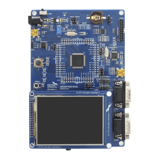
GigaDevice Semiconductor GD32VF103 User Manual (536 pages)
RISC-V 32-bit MCU
Brand:
GigaDevice Semiconductor
| Category:
Microcontrollers
| Size: 10 MB
Table of Contents
Table of Contents
2
List of Figures
14
List of Tables
20
1 System and Memory Architecture
22
Risc-V Cpu
22
System Architecture
22
Table 1-1. the Interconnection Relationship of the AHB Interconnect Matrix
23
Figure 1-1. GD32VF103 System Architecture
24
Memory Map
24
Table 1-2. Memory Map of GD32VF103 Devices
25
Table 1-3. Boot Modes
29
Table 2-1. Base Address and Size for Flash Memory
32
Page Erase
33
Read Operations
33
Unlock the FMC_CTL Registers
33
Memory Density Information
30
Unique Device ID (96 Bits)
30
On-Chip Flash Memory Overview
28
On-Chip SRAM Memory
28
Boot Configuration
29
Device Electronic Signature
29
2 Flash Memory Controller (FMC)
32
Characteristics
32
Function Overview
32
Flash Memory Architecture
32
Overview
32
Figure 2-1. Process of Page Erase Operation
34
Figure 2-2. Process of Mass Erase Operation
35
Figure 2-3. Process of Word Program Operation
37
Option Bytes Erase
37
Option Bytes Description
38
Option Bytes Modify
38
Table 2-2. Option Byte
38
Page Erase/Program Protection
39
Security Protection
40
Register Definition
41
Unlock Key Register (FMC_KEY)
41
Wait State Register (FMC_WS)
41
Option Byte Unlock Key Register (FMC_OBKEY)
42
Status Register (FMC_STAT)
42
Control Register (FMC_CTL)
43
Address Register (FMC_ADDR)
44
Erase/Program Protection Register (FMC_WP)
45
Option Byte Status Register (FMC_OBSTAT)
45
Product ID Register (FMC_PID)
46
Main Flash Programming
35
Mass Erase
34
3 Power Management Unit (PMU)
47
Characteristics
47
Figure 3-1. Power Supply Overview
47
Function Overview
47
Overview
47
Battery Backup Domain
48
VDD /V Dda
48
Figure 3-2. Waveform of the POR/PDR
49
Figure 3-3. Waveform of the LVD Threshold
50
Table 3-1. Power Saving Mode Summary
52
Register Definition
54
Control Register (PMU_CTL)
54
Control and Status Register (PMU_CS)
55
Power Domain
51
Power Saving Modes
51
4 Backup Registers (BKP)
57
Overview
57
Characteristics
57
Function Overview
57
RTC Clock Calibration
57
Tamper Detection
58
Register Definition
59
Backup Data Register X (Bkp_Datax) (X= 0
59
RTC Signal Output Control Register (BKP_OCTL)
59
Tamper Pin Control Register (BKP_TPCTL)
60
Tamper Control and Status Register (BKP_TPCS)
60
5 Reset and Clock Unit (RCU)
62
Reset Control Unit (RCTL)
62
Overview
62
Function Overview
62
Clock Control Unit (CCTL)
63
Figure 5-1. the System Reset Circuit
63
Figure 5-2. Clock Tree
64
Figure 5-3. HXTAL Clock Source
65
Function Overview
65
Overview
63
Table 5-1. Clock Output 0 Source Select
68
Table 5-2. 1.2V Domain Voltage Selected in Deep-Sleep Mode
68
Register Definition
69
Control Register (RCU_CTL)
69
Clock Configuration Register 0 (RCU_CFG0)
71
Clock Interrupt Register (RCU_INT)
74
APB2 Reset Register (RCU_APB2RST)
77
APB1 Reset Register (RCU_APB1RST)
79
AHB Enable Register (RCU_AHBEN)
82
APB2 Enable Register (RCU_APB2EN)
83
APB1 Enable Register (RCU_APB1EN)
85
Backup Domain Control Register (RCU_BDCTL)
87
Reset Source/Clock Register (RCU_RSTSCK)
88
AHB Reset Register (RCU_AHBRST)
90
Clock Configuration Register 1 (RCU_CFG1)
91
Deep-Sleep Mode Voltage Register (RCU_DSV)
93
Characteristics
65
6 Interrupt/Event Controller (EXTI)
94
Characteristics
94
Function Overview
94
Overview
94
Table 6-1. Interrupt Vector Table
95
External Interrupt and Event (EXTI) Block Diagram
97
External Interrupt and Event Function Overview
97
Figure 6-1. Block Diagram of EXTI
97
Table 6-2. EXTI Source
98
Table 7.1. GPIO Configuration Table
102
GPIO Pin Configuration
103
Register Definition
99
Interrupt Enable Register (EXTI_INTEN)
99
Event Enable Register (EXTI_EVEN)
99
Rising Edge Trigger Enable Register (EXTI_RTEN)
100
Falling Edge Trigger Enable Register (EXTI_FTEN)
100
Software Interrupt Event Register (EXTI_SWIEV)
101
Pending Register (EXTI_PD)
101
7 General-Purpose and Alternate-Function I/Os (GPIO and AFIO)
102
Characteristics
102
Function Overview
102
Overview
102
Figure 7.1. Basic Structure of a Standard I/O Port Bit
103
Figure 7.2. Input Configuration
104
Figure 7.3. Output Configuration
105
Alternate Function (AF) Configuration
106
Analog Configuration
106
Output Configuration
105
Alternate Functions (AF)
104
External Interrupt/Event Lines
104
Input Configuration
104
Figure 7.5. Alternate Function Configuration
106
Figure 7.4. Analog Configuration
106
GPIO Locking Function
107
IO Pin Function Selection
107
Remapping Function I/O and Debug Configuration
108
Introduction
108
JTAG Alternate Function Remapping
108
Main Features
108
Table 7.2. Debug Interface Signals
108
Table 7.3. Debug Port Mapping
108
Table 7.4. TIMER0 Alternate Function Remapping
109
Table 7.6. TIMER2 Alternate Function Remapping
109
Table 7.7. TIMER3 Alternate Function Remapping
109
Table 7.8. TIMER4 Alternate Function Remapping
110
Table 7.9. USART0 Alternate Function Remapping
110
USART AF Remapping
110
CAN0 AF Remapping
111
CAN1 AF Remapping
111
SPI0 AF Remapping
111
SPI2/I2S2 AF Remapping
111
Table 7.5. TIMER1 Alternate Function Remapping
109
TIMER AF Remapping
109
I2C0 AF Remapping
110
Table 7.11. USART2 Alternate Function Remapping
110
Table 7.12. I2C0 Alternate Function Remapping
110
Table 7.13. SPI0 Alternate Function Remapping
111
Table 7.15. CAN0 Alternate Function Remapping
111
Table 7.17. OSC32 Pins Configuration
112
Table 7.18. OSC Pins Configuration
112
Figure 8-1. Block Diagram of CRC Calculation Unit
129
Function Overview
130
Data Register (CRC_DATA)
131
Free Data Register (CRC_FDATA)
131
Register Definition
131
Control Register (CRC_CTL)
132
Table 7.16. CAN1 Alternate Function Remapping
111
Register Definition
113
Port Control Register 0 (Gpiox_Ctl0, X=A
113
Port Control Register 1 (Gpiox_Ctl1, X=A
115
Port Input Status Register (Gpiox_Istat, X=A
116
Port Bit Operate Register (Gpiox_Bop, X=A
117
Port Output Control Register (Gpiox_Octl, X=A
117
Port Bit Clear Register (Gpiox_Bc, X=A
118
Port Configuration Lock Register (Gpiox_Lock, X=A
118
Event Control Register (AFIO_EC)
119
AFIO Port Configuration Register 0 (AFIO_PCF0)
120
EXTI Sources Selection Register 0 (AFIO_EXTISS0)
123
EXTI Sources Selection Register 1 (AFIO_EXTISS1)
124
EXTI Sources Selection Register 2 (AFIO_EXTISS2)
125
EXTI Sources Selection Register 3 (AFIO_EXTISS3)
126
AFIO Port Configuration Register 1 (AFIO_PCF1)
127
Table 7.10. USART1 Alternate Function Remapping
110
Table 7.14. SPI2/I2S2 Alternate Function Remapping
111
CLK Pins AF Remapping
112
8 CRC Calculation Unit (CRC)
129
Overview
129
Characteristics
129
9 Direct Memory Access Controller (DMA)
133
Characteristics
133
Overview
133
Block Diagram
134
Figure 9-1. Block Diagram of DMA
134
Function Overview
134
DMA Operation
134
Table 9-1. DMA Transfer Operation
135
Figure 9-2. Handshake Mechanism
136
Figure 9-3. DMA Interrupt Logic
138
Interrupt
138
Table 9-2. Interrupt Events
138
DMA Request Mapping
139
Peripheral Handshake
136
Address Generation
137
Channel Configuration
137
Circular Mode
137
Memory to Memory Mode
137
Arbitration
136
Table 9-4. DMA1 Requests for each Channel
139
Table 9-3. DMA0 Requests for each Channel
139
Figure 9-4. DMA0 Request Mapping
139
Figure 9-5. DMA1 Request Mapping
140
Register Definition
142
Interrupt Flag Register (DMA_INTF)
142
Interrupt Flag Clear Register (DMA_INTC)
143
Channel X Control Register (Dma_Chxctl)
143
Channel X Counter Register (Dma_Chxcnt)
145
Channel X Peripheral Base Address Register (Dma_Chxpaddr)
146
Channel X Memory Base Address Register (Dma_Chxmaddr)
146
10 Debug (DBG)
148
Overview
148
JTAG Function Overview
148
Pin Assignment
148
JTAG Daisy Chained Structure
148
Debug Reset
149
Debug Hold Function Overview
149
Debug Support for Power Saving Mode
149
Debug Support for TIMER, I2C, WWDGT, FWDGT and CAN
149
Register Definition
150
ID Code Register (DBG_ID)
150
Control Register (DBG_CTL)
150
11 Analog-To-Digital Converter (ADC)
153
Introduction
153
Main Features
153
Figure 11-1. ADC Module Block Diagram
154
Functional Description
154
Pins and Internal Signals
154
Table 11-1. ADC Internal Signals
154
Table 11-2. ADC Pins Definition
154
Calibration (CLB)
155
ADC Clock
156
ADCON Switch
156
Conversion Modes
156
Figure 11-2. Single Conversion Mode
156
Figure 11-18. Trigger Rotation: Inserted Channel Group
171
Figure 11-20. Regular Parallel & Trigger Rotation Mode
172
Figure 11-22 Follow-Up Single Channel with Inserted Sequence CH1, CH2
172
Figure 12-1. DAC Block Diagram
188
DAC Enable
189
Function Overview
189
Figure 11-21. Trigger Occurs During Inserted Conversion
172
ADC Interrupts
173
ADC Registers
174
Status Register (ADC_STAT)
174
Control Register 0 (ADC_CTL0)
175
Control Register 1 (ADC_CTL1)
177
Sample Time Register 0 (ADC_SAMPT0)
179
Sample Time Register 1 (ADC_SAMPT1)
180
Inserted Channel Data Offset Register X (Adc_Ioffx) (X=0
181
Watchdog High Threshold Register (ADC_WDHT)
181
Regular Sequence Register 0 (ADC_RSQ0)
182
Watchdog Low Threshold Register (ADC_WDLT)
182
Regular Sequence Register 1 (ADC_RSQ1)
183
Regular Sequence Register 2 (ADC_RSQ2)
183
Inserted Sequence Register (ADC_ISQ)
184
Inserted Data Register X (Adc_Idatax) (X= 0
185
Regular Data Register (ADC_RDATA)
185
Oversample Control Register (ADC_OVSAMPCTL)
186
Regular and Inserted Channel Groups
156
Figure 11-3. Continuous Conversion Mode
157
Figure 11-4. Scan Conversion Mode, Continuous Disable
158
Figure 11-5. Scan Conversion Mode, Continuous Enable
159
Figure 11-6. Discontinuous Conversion Mode
160
Data Alignment
161
Figure 11-7. Auto-Insertion, CNT = 1
161
Figure 11-8. Triggered Insertion
161
Figure 11-10. 6-Bit Data Alignment
162
Figure 11-9. 12-Bit Data Alignment
162
DMA Request
163
External Trigger
163
Refint
163
Table 11-3. External Trigger for Regular Channels for ADC0 and ADC1
163
Table 11-4. External Trigger for Inserted Channels for ADC0 and ADC1
163
Temperature Sensor, and Internal Reference Voltage V
163
Programmable Resolution (DRES) - Fast Conversion Mode
164
Table 11-5. T CONV Timings Depending on Resolution
164
Figure 11-11. 20-Bit to 16-Bit Result Truncation
165
Figure 11-12. Numerical Example with 5-Bits Shift and Rounding
165
On-Chip Hardware Oversampling
165
ADC Sync Mode
166
Table 11-6. Maximum Output Results Vs N and M (Grayed Values Indicates Truncation)
166
Figure 11-13. ADC Sync Block Diagram
167
Free Mode
167
Figure 11-14. Regular Parallel Mode on 16 Channels
168
Inserted Parallel Mode
168
Regular Parallel Mode
168
Figure 11-15. Inserted Parallel Mode on 4 Channels
169
Figure 11-16. Follow-Up Fast Mode on 1 Channel in Continuous Conversion Mode
169
Follow-Up Fast Mode
169
Follow-Up Slow Mode
169
Figure 11-17. Follow-Up Slow Mode on 1 Channel
170
Trigger Rotation Mode
170
Combined Regular Parallel & Inserted Parallel Mode
171
Combined Regular Parallel & Trigger Rotation Mode
171
Figure 11-19. Trigger Rotation: Inserted Channels in Discontinuous Mode
171
Combined Inserted Parallel & Follow-Up Mode
172
Programmable Sample Time
162
Inserted Channel Management
160
12 Digital-To-Analog Converter (DAC)
188
Characteristics
188
Overview
188
Table 12-1. DAC Pins
189
Table 12-2. External Triggers of DAC
190
DAC Noise Wave
191
DAC Conversion
190
DAC Data Configuration
190
DAC Output Buffer
190
DAC Trigger
190
Figure 12-3. DAC Triangle Noise Wave
191
Figure 12-2. DAC LFSR Algorithm
191
DAC Concurrent Conversion
192
DAC Output Voltage
192
DMA Request
192
Register Definition
193
Control Register (DAC_CTL)
193
Software Trigger Register (DAC_SWT)
195
DAC0 12-Bit Right-Aligned Data Holding Register (DAC0_R12DH)
196
DAC0 12-Bit Left-Aligned Data Holding Register (DAC0_L12DH)
196
DAC0 8-Bit Right-Aligned Data Holding Register (DAC0_R8DH)
197
DAC1 12-Bit Right-Aligned Data Holding Register (DAC1_R12DH)
197
DAC1 12-Bit Left-Aligned Data Holding Register (DAC1_L12DH)
198
DAC1 8-Bit Right-Aligned Data Holding Register (DAC1_R8DH)
198
DAC Concurrent Mode 12-Bit Right-Aligned Data Holding Register (DACC_R12DH)
199
DAC Concurrent Mode 12-Bit Left-Aligned Data Holding Register (DACC_L12DH)
199
DAC Concurrent Mode 8-Bit Right-Aligned Data Holding Register (DACC_R8DH)
200
DAC0 Data Output Register (DAC0_DO)
200
DAC1 Data Output Register (DAC1_DO)
201
13 Watchdog Timer (WDGT)
202
Free Watchdog Timer (FWDGT)
202
Overview
202
Characteristics
202
Function Overview
202
Table 13.1. Min/Max FWDGT Timeout Period at 40 Khz (IRC40K)
203
Figure 13.1. Free Watchdog Block Diagram
203
Register Definition
205
Window Watchdog Timer (WWDGT)
208
Overview
208
Characteristics
208
Function Overview
208
Figure 13.2. Window Watchdog Timer Block Diagram
209
Table 13.2. Min/Max Timeout Value at 54 Mhz
210
Register Definition
211
Figure 13.3. Window Watchdog Timing Diagram
210
14 Real-Time Clock (RTC)
213
Characteristics
213
Function Overview
213
RTC Reset
214
RTC Reading
214
Overview
213
Figure 14.1. Block Diagram of RTC
214
Figure 14.2. RTC Second and Alarm Waveform Example (RTC_PSC = 3, RTC_ALRM = 2)
215
Figure 14.3. RTC Second and Overflow Waveform Example (RTC_PSC= 3)
216
Table 15-1. Timers (Timerx) Are Devided into Three Sorts
222
Advanced Timer (Timerx, X=0)
223
Characteristics
223
Overview
223
Block Diagram
224
Function Overview
224
Register Definition
217
RTC Control Register(RTC_CTL)
217
RTC Interrupt Enable Register(RTC_INTEN)
217
RTC Prescaler High Register (RTC_PSCH)
218
RTC Divider High Register (RTC_DIVH)
219
RTC Divider Low Register (RTC_DIVL)
219
RTC Prescaler Low Register (RTC_PSCL)
219
RTC Counter High Register (RTC_CNTH)
220
RTC Counter Low Register (RTC_CNTL)
220
RTC Alarm High Register (RTC_ALRMH)
221
RTC Alarm Low Register (RTC_ALRML)
221
RTC Configuration
215
RTC Flag Assertion
215
15 Timer(Timerx)
222
Figure 15-1. Advanced Timer Block Diagram
224
Figure 15-2. Normal Mode, Internal Clock Divided by 1
225
Figure 15-3. Counter Timing Diagram with Prescaler Division Change from 1 to 2
226
Figure 15-5. Timing Chart of up Counting Mode, Change Timerx_Car Ongoing
228
Figure 15-6. Timing Chart of down Counting Mode, PSC=0/1
228
Figure 15-7. Timing Chart of down Counting Mode, Change Timerx_Car Ongoing
230
Figure 15-8. Timing Chart of Center-Aligned Counting Mode
231
Figure 15-9. Repetition Counter Timing Chart of Center-Aligned Counting Mode
232
Figure 15-11. Repetition Counter Timing Chart of down Counting Mode
233
Figure 15-12. Input Capture Logic
234
Figure 15-13. Output Compare Logic (with Complementary Output, X=0,1,2)
235
Figure 15-14. Output Compare Logic (CH3_O)
235
Figure 15-15. Output-Compare in Three Modes
236
Figure 15-16. Timing Chart of EAPWM
237
Figure 15-17. Timing Chart of CAPWM
238
Table 15-2. Complementary Outputs Controlled by Parameters
240
Figure 15-18. Complementary Output with Dead Time Insertion
241
Figure 15-19. Output Behavior of the Channel in Response to a Break (the Break High Active)
242
Figure 15-21. Example of Encoder Interface Mode with CI0FE0 Polarity Inverted
243
Table 15-3. Counting Direction Versus Encoder Signals
243
Figure 15-22. Hall Sensor Is Used to BLDC Motor
244
Table 15-4. Slave Mode Example Table
245
Figure 15-24. Restart Mode
246
Figure 15-25. Pause Mode
246
Figure 15-26. Event Mode
247
Figure 15-27. Single Pulse Mode Timerx_Chxcv=0X04, Timerx_Car=0X60
248
Figure 15-29. Triggering TIMER0 with Enable Signal of TIMER2
249
Figure 15-30. Triggering TIMER0 with Update Signal of TIMER2
250
Figure 15-31. Pause TIMER0 with Enable Signal of TIMER2
251
Figure 15-32. Pause TIMER0 with O0CPREF Signal of Timer2
251
Figure 15-33. Triggering TIMER0 and TIMER2 with Timer2'S CI0 Input
252
Figure 15-34. General Level 0 Timer Block Diagram
279
Function Overview
280
Figure 15-35. Normal Mode, Internal Clock Divided by 1
281
Figure 15-36. Counter Timing Diagram with Prescaler Division Change from 1 to 2
282
Figure 15-38. Timing Chart of up Counting Mode, Change Timerx_Car Ongoing
284
Figure 15-39. Timing Chart of down Counting Mode, PSC=0/1
285
Figure 15-40. Timing Chart of down Counting Mode, Change Timerx_Car
286
Figure 15-41. Timing Chart of Center-Aligned Counting Mode
287
Figure 15-42. Input Capture Logic
288
Figure 15-43. Output-Compare in Three Modes
290
Figure 15-44. EAPWM Timechart
290
Figure 15-45. CAPWM Timechart
290
Table 15-5. Counting Direction Versus Encoder Signals
292
Figure 15-46. Example of Counter Operation in Encoder Interface Mode
293
Figure 15-47. Example of Encoder Interface Mode with CI0FE0 Polarity Inverted
293
Figure 15-48. Restart Mode
294
Table 15-6. Slave Controller Examples
294
Figure 15-52. Basic Timer Block Diagram
318
Figure 15-53. Normal Mode, Internal Clock Divided by 1
319
Figure 15-54. Counter Timing Diagram with Prescaler Division Change from 1 to 2
320
Figure 15-55. Timing Chart of up Counting Mode, PSC=0/1
320
Figure 15-56. Timing Chart of up Counting Mode, Change Timerx_Car Ongoing
322
Timerx Registers(X=5,6)
323
Figure 15-37. Timing Chart of up Counting Mode, PSC=0/1
282
Figure 15-49. Pause Mode
295
Figure 15-50. Event Mode
295
Figure 15-51. Single Pulse Mode Timerx_Chxcv = 0X04 Timerx_Car=0X60
296
Timerx Registers(X=1,2,3,4)
297
Basic Timer (Timerx, X=5, 6)
318
Block Diagram
318
Characteristics
318
Function Overview
318
Overview
318
Figure 15-4. Timing Chart of up Counting Mode, PSC=0/1
226
Figure 15-10. Repetition Counter Timing Chart of up Counting Mode
232
Figure 15-20. Example of Counter Operation in Encoder Interface Mode
243
Figure 15-23. Hall Sensor Timing between Two Timers
245
Figure 15-28. TIMER0 Master/Slave Mode Timer Example
248
Timerx Registers(X=0)
254
General Level0 Timer (Timerx, X=1, 2, 3, 4)
279
Overview
279
Characteristics
279
Block Diagram
279
16 Universal Synchronous/Asynchronous Receiver /Transmitter (USART)
328
Characteristics
328
Overview
328
Function Overview
329
Table 16-1. Description of USART Important Pins
329
Figure 16-1. USART Module Block Diagram
330
Figure 16-2. USART Character Frame (8 Bits Data and 1 Stop Bit)
330
Table 16-2. Stop Bits Configuration
330
Figure 16-3. USART Transmit Procedure
332
Figure 16-4. Receiving a Frame Bit by Oversampling Method
333
Figure 16-5. Configuration Steps When Using DMA for USART Transmission
334
Figure 16-6. Configuration Steps When Using DMA for USART Reception
335
Hardware Flow Control
335
Multi-Processor Communication
336
Baud Rate Generation
331
USART Transmitter
331
Use DMA for Data Buffer Access
334
Figure 16-7. Hardware Flow Control between Two Usarts
336
Figure 16-8. Hardware Flow Control
336
Figure 16-10. Break Frame Occurs During a Frame
338
Figure 16-9. Break Frame Occurs During Idle State
338
Irda SIR ENDEC Mode
339
LIN Mode
337
Synchronous Mode
338
USART Frame Format
330
USART Receiver
333
Figure 16-12. 8-Bit Format USART Synchronous Waveform (CLEN=1)
339
Figure 16-14. Irda Data Modulation
340
Figure 16-13. Irda SIR ENDEC Module
340
Figure 16-15. ISO7816-3 Frame Format
341
Table 16-3. USART Interrupt Requests
342
USART Interrupts
342
Figure 16-16. USART Interrupt Mapping Diagram
343
Register Definition
344
Status Register (USART_STAT)
344
Baud Rate Register (USART_BAUD)
346
Data Register (USART_DATA)
346
Control Register 0 (USART_CTL0)
347
Control Register 1 (USART_CTL1)
349
Control Register 2 (USART_CTL2)
350
Guard Time and Prescaler Register (USART_GP)
352
Figure 16-11. Example of USART in Synchronous Mode
339
Half-Duplex Communication Mode
341
Smartcard (ISO7816-3) Mode
341
17 Inter-Integrated Circuit Interface (I2C)
354
Characteristics
354
Figure 17-1. I2C Module Block Diagram
354
Table 17-1. Definition of I2C-Bus Terminology (Refer to the I2C Specification of Philips Semiconductors)
355
Clock Synchronization
356
Data Validation
356
START and STOP Condition
356
Function Overview
354
Overview
354
SDA and SCL Lines
355
Figure 17-2. Data Validation
356
Figure 17-3. START and STOP Condition
356
Figure 17-5. SDA Line Arbitration
357
Figure 17-4. Clock Synchronization
357
Programming Model
358
Arbitration
357
I2C Communication Flow
357
Figure 17-7. I2C Communication Flow with 10-Bit Address (Master Transmit)
358
Figure 17-8. I2C Communication Flow with 10-Bit Address (Master Receive)
358
Figure 17-10. Programming Model for Slave Receiving(10-Bit Address Mode)
360
Figure 17-9. Programming Model for Slave Transmitting(10-Bit Address Mode)
360
Figure 17-11. Programming Model for Master Transmitting(10-Bit Address Mode)
363
Figure 17-12. Programming Model for Master Receiving Using Solution a(10-Bit Address Mode)
365
Figure 17-13. Programming Model for Master Receiving Using Solution B(10-Bit Address Mode)
367
Packet Error Checking
368
Smbus Support
368
Use DMA for Data Transfer
368
Status, Errors and Interrupts
370
Table17-2. Event Status Flags
370
Table17-3. I2C Error Flags
370
Register Definition
371
Control Register 0 (I2C_CTL0)
371
Control Register 1 (I2C_CTL1)
373
Slave Address Register 0 (I2C_SADDR0)
374
Slave Address Register 1 (I2C_SADDR1)
374
Transfer Buffer Register (I2C_DATA)
375
Transfer Status Register 0 (I2C_STAT0)
375
Transfer Status Register 1 (I2C_STAT1)
377
Clock Configure Register (I2C_CKCFG)
378
Rise Time Register (I2C_RT)
379
Figure 17-6. I2C Communication Flow with 7-Bit Address
358
SCL Line Stretching
367
18 Serial Peripheral Interface/Inter-IC Sound (SPI/I2S)
380
Characteristics
380
SPI Characteristics
380
I2S Characteristics
380
Overview
380
Figure 18-1. Block Diagram of SPI
381
SPI Block Diagram
381
SPI Signal Description
381
Normal Configuration
381
Table 18-1. SPI Signal Description
381
Figure 18-2. SPI Timing Diagram in Normal Mode
382
SPI Operating Modes
383
SPI Function Overview
382
NSS Function
382
SPI Clock Timing and Data Format
382
Table 18-2. SPI Operating Modes
383
Figure 18-5. a Typical Simplex Connection (Master: Transmit Only, Slave: Receive)
384
Figure 18-3. a Typical Full-Duplex Connection
384
Figure 18-4. a Typical Simplex Connection (Master: Receive, Slave: Transmit)
384
Figure 18-6. a Typical Bidirectional Connection
385
Figure 18-7. Timing Diagram of TI Master Mode with Discontinuous Transfer
386
Figure 18-9. Timing Diagram of TI Slave Mode
387
Figure 18-8. Timing Diagram of TI Master Mode with Continuous Transfer
387
Table 18-3. SPI Interrupt Requests
390
Figure 18-11. Block Diagram of I2S
391
I2S Block Diagram
391
I2S Signal Description
391
I2S Function Overview
392
I2S Audio Standards
392
Figure 18-10. Timing Diagram of NSS Pulse with Continuous Transmission
388
CRC Function
389
DMA Function
389
SPI Interrupts
389
Status Flags
389
Error Flags
390
Figure 18-12. I2S Phillips Standard Timing Diagram (DTLEN=00, CHLEN=0, CKPL=0)
392
Figure 18-13. I2S Phillips Standard Timing Diagram (DTLEN=00, CHLEN=0, CKPL=1)
392
Figure 18-15. I2S Phillips Standard Timing Diagram (DTLEN=10, CHLEN=1, CKPL=1)
393
Figure 18-16. I2S Phillips Standard Timing Diagram (DTLEN=01, CHLEN=1, CKPL=0)
393
Figure 18-17. I2S Phillips Standard Timing Diagram (DTLEN=01, CHLEN=1, CKPL=1)
393
Figure 18-18. I2S Phillips Standard Timing Diagram (DTLEN=00, CHLEN=1, CKPL=0)
394
Figure 18-20. MSB Justified Standard Timing Diagram (DTLEN=00, CHLEN=0, CKPL=0)
394
Figure 18-21. MSB Justified Standard Timing Diagram (DTLEN=00, CHLEN=0, CKPL=1)
394
Figure 18-22. MSB Justified Standard Timing Diagram (DTLEN=10, CHLEN=1, CKPL=0)
394
Figure 18-24. MSB Justified Standard Timing Diagram (DTLEN=01, CHLEN=1, CKPL=0)
395
Figure 18-27. MSB Justified Standard Timing Diagram (DTLEN=00, CHLEN=1, CKPL=1)
395
Figure 18-29. LSB Justified Standard Timing Diagram (DTLEN=01, CHLEN=1, CKPL=1)
396
Figure 18-30. LSB Justified Standard Timing Diagram (DTLEN=00, CHLEN=1, CKPL=0)
396
Figure 18-33. PCM Standard Short Frame Synchronization Mode Timing Diagram
397
Figure 18-34. PCM Standard Short Frame Synchronization Mode Timing Diagram (DTLEN=10, CHLEN=1, CKPL=0)
397
Figure 18-35. PCM Standard Short Frame Synchronization Mode Timing Diagram (DTLEN=10, CHLEN=1, CKPL=1)
397
Figure 18-38. PCM Standard Short Frame Synchronization Mode Timing Diagram
397
Figure 18-39. PCM Standard Short Frame Synchronization Mode Timing Diagram
397
Figure 18-40. PCM Standard Long Frame Synchronization Mode Timing Diagram (DTLEN=00, CHLEN=0, CKPL=0)
398
Figure 18-41. PCM Standard Long Frame Synchronization Mode Timing Diagram
399
Figure 18-43. PCM Standard Long Frame Synchronization Mode Timing Diagram (DTLEN=10, CHLEN=1, CKPL=1)
399
Figure 18-47. PCM Standard Long Frame Synchronization Mode Timing Diagram (DTLEN=00, CHLEN=1, CKPL=1)
399
Table 18-4. I2S Bitrate Calculation Formulas
400
Table 18-5. Audio Sampling Frequency Calculation Formulas
400
Table 18-6. Direction of I2S Interface Signals for each Operation Mode
401
DMA Function
403
Error Flags
404
I2S Interrupts
404
Status Flags
404
Table 18-7. I2S Interrupt
405
Control Register 0 (SPI_CTL0)
406
Register Definition
406
Control Register 1 (SPI_CTL1)
408
Status Register (SPI_STAT)
409
Data Register (SPI_DATA)
410
CRC Polynomial Register (SPI_CRCPOLY)
411
RX CRC Register (SPI_RCRC)
411
TX CRC Register (SPI_TCRC)
412
I2S Control Register (SPI_I2SCTL)
413
I2S Clock Prescaler Register (SPI_I2SPSC)
414
Figure 18-14. I2S Phillips Standard Timing Diagram (DTLEN=10, CHLEN=1, CKPL=0)
393
Figure 18-23. MSB Justified Standard Timing Diagram (DTLEN=10, CHLEN=1, CKPL=1)
395
Figure 18-32. PCM Standard Short Frame Synchronization Mode Timing Diagram (DTLEN=00, CHLEN=0, CKPL=0)
397
Figure 18-42. PCM Standard Long Frame Synchronization Mode Timing Diagram
399
Operation
401
Figure 18-19. I2S Phillips Standard Timing Diagram (DTLEN=00, CHLEN=1, CKPL=1)
394
Figure 18-26. MSB Justified Standard Timing Diagram (DTLEN=00, CHLEN=1, CKPL=0)
395
Figure 18-25. MSB Justified Standard Timing Diagram (DTLEN=01, CHLEN=1, CKPL=1)
395
Figure 18-31. LSB Justified Standard Timing Diagram (DTLEN=00, CHLEN=1, CKPL=1)
396
Figure 18-28. LSB Justified Standard Timing Diagram (DTLEN=01, CHLEN=1, CKPL=0)
396
Figure 18-36. PCM Standard Short Frame Synchronization Mode Timing Diagram (DTLEN=01, CHLEN=1, CKPL=0)
397
Figure 18-37. PCM Standard Short Frame Synchronization Mode Timing Diagram
397
Figure 18-45. PCM Standard Long Frame Synchronization Mode Timing Diagram (DTLEN=01, CHLEN=1, CKPL=1)
399
Figure 18-44. PCM Standard Long Frame Synchronization Mode Timing Diagram (DTLEN=01, CHLEN=1, CKPL=0)
399
Figure 18-46. PCM Standard Long Frame Synchronization Mode Timing Diagram (DTLEN=00, CHLEN=1, CKPL=0)
399
Figure 18-48. Block Diagram of I2S Clock Generator
400
I2S Clock
400
19 External Memory Controller (EXMC)
416
Characteristics
416
Function Overview
416
Block Diagram
416
Basic Regulation of EXMC Access
417
Overview
416
Figure 19-1. the EXMC Block Diagram
417
External Device Address Mapping
418
Figure 19-3. Region of Bank0 Address Mapping
418
Figure 19-2. EXMC Memory Banks
418
NOR/PSRAM Controller
418
Table 19-1. nor Flash Interface Signals Description
419
Table 19-3. EXMC Bank 0 Supports All Transactions
419
Table 19-2. PSRAM Muxed Signal Description
419
Table 19-4. nor / PSRAM Controller Timing Parameters
420
Figure 19-5. Multiplex Mode Write Access
421
Figure 19-4. Multiplex Mode Read Access
421
Table 19-5. Exmc_Timing Models
421
Table 19-6. Multiplex Mode Related Registers Configuration
422
Figure 19-7. Write Access Timing Diagram under Async-Wait Signal Assertion
423
Figure 19-6. Read Access Timing Diagram under Async-Wait Signal Assertion
423
Register Definition
424
NOR/PSRAM Controller Registers
424
20 Controller Area Network (CAN)
427
Characteristics
427
Overview
427
Figure 20-1. CAN Module Block Diagram
428
Function Overview
428
Working Mode
428
Communication Modes
429
Data Transmission
430
Figure 20-2. Transmission Register
430
Figure 20-3. State of Transmission Mailbox
431
Figure 20-4. Reception Register
432
Filtering Function
433
Data Reception
432
Figure 20-6. 16-Bit Filter
434
Figure 20-7. 32-Bit Mask Mode Filter
434
Table 20-2. Filtering Index
435
Table 20-1. 32-Bit Filter Number
435
Figure 20-11. the Bit Time
438
CAN Interrupts
439
Register Definition
441
Control Register (CAN_CTL)
441
Status Register (CAN_STAT)
442
Transmit Status Register (CAN_TSTAT)
444
Receive Message FIFO0 Register (CAN_RFIFO0)
447
Receive Message FIFO1 Register (CAN_RFIFO1)
447
Interrupt Enable Register (CAN_INTEN)
448
Error Register (CAN_ERR)
450
Bit Timing Register (CAN_BT)
451
Transmit Mailbox Identifier Register (Can_Tmix) (X=0
452
Transmit Mailbox Data0 Register (Can_Tmdata0X) (X=0
453
Transmit Mailbox Property Register (Can_Tmpx) (X=0
453
Receive FIFO Mailbox Identifier Register (Can_Rfifomix) (X=0,1)
454
Transmit Mailbox Data1 Register (Can_Tmdata1X) (X=0
454
Receive FIFO Mailbox Property Register (Can_Rfifompx) (X=0,1)
455
Receive FIFO Mailbox Data0 Register (Can_Rfifomdata0X) (X=0,1)
456
Receive FIFO Mailbox Data1 Register (Can_Rfifomdata1X) (X=0,1)
456
Filter Control Register (CAN_FCTL)
457
Filter Mode Configuration Register (CAN_FMCFG)
457
Filter Associated FIFO Register (CAN_FAFIFO)
458
Filter Scale Configuration Register (CAN_FSCFG)
458
Filter Working Register (CAN_FW)
459
Filter X Data y Register (Can_Fxdatay) (X=0
459
Figure 20-5. 32-Bit Filter
434
Figure 20-10. 16-Bit List Mode Filter
434
Figure 20-9. 32-Bit List Mode Filter
434
Figure 20-8. 16-Bit Mask Mode Filter
434
Time-Triggered Communication
436
Communication Parameters
437
Error Flags
438
21 Universal Serial Bus Full-Speed Interface (USBFS)
461
Characteristics
461
Overview
461
Block Diagram
462
Figure 21-1. USBFS Block Diagram
462
Function Overview
462
USBFS Clocks and Working Modes
462
Signal Description
462
Table 21-1. USBFS Signal Description
462
Figure 21-5. HOST Mode FIFO Space in SRAM
469
Figure 21-6. Host Mode FIFO Access Register Map
469
Figure 21-7. Device Mode FIFO Space in SRAM
470
Figure 21-8. Device Mode FIFO Access Register Map
471
Table 21-2. USBFS Global Interrupt
475
Global Control and Status Registers
477
Register Definition
477
Host Control and Status Registers
498
Device Control and Status Registers
510
Power and Clock Control Register (USBFS_PWRCLKCTL)
534
Operation Guide
471
Interrupts
475
Figure 21-2. Connection with Host or Device Mode
463
Figure 21-3. Connection with OTG Mode
464
Figure 21-4. State Transition Diagram of Host Port
464
USB Host Function
464
USB Device Function
466
OTG Function Overview
467
Data FIFO
468
22 Revision History
535
Table 22-1. Revision History
535
Advertisement
GigaDevice Semiconductor GD32VF103 User Manual (65 pages)
Brand:
GigaDevice Semiconductor
| Category:
Computer Hardware
| Size: 2 MB
Table of Contents
Table of Contents
2
List of Figures
4
List of Tables
5
Introduction
7
Table 1-1. Applicable Products
7
Library Architecture and File Structure
8
Library Architecture
8
Figure 2-1. GD32 USBFS Firmware Library Framework
8
File Structure
9
Figure 2-2. USBFS Firmware Library Folder
9
Figure 2-3. Device Folder
9
Figure 2-4. Driver Folder
10
Figure 2-5. Host Folder
10
Figure 2-6. Ustd Folder
11
USBFS Bottom Driver
12
Table 3-1. USBFS Underlying File
12
Table 3-2. Usb_Core.h/.C File Function
12
USBFS Middle Layer Driver
13
Host Middle Layer Driver Function
13
Table 4-1. USBFS Middle Layer Driver File
13
Table 4-2. Drv_Usb_Host.h/.C File Function
13
Table 4-3. Drv_Usbh_Int.h/.C File Function
13
Table 4-4. Usbh_Core.h/.C File Function
14
Table 4-5. Usbh_Enum.h/.C File Function
14
Table 4-6. Usbh_Pipe.h/.C File Function
14
Device Middle Layer Driver Function
15
Table 4-7. Usbh_Transc.h/.C File Function
15
Table 4-8. Drv_Usb_Dev.h/.C File Function
15
Table 4-9. Drv_Usbd_Int.h/.C File Function
16
Table 4-10. Usbd_Core.h/.C File Function
16
Table 4-11. Usbd_Enum.h/.C File Function
16
Table 4-12. Usbd_Transc.h/.C File Function
17
USBFS Device Library
18
Device Library Configuration
18
Usbd_Conf.h
18
Usb_Conf.h
18
Table 5-1. Usbd_Conf.h Configuration Description
18
Firmware Library Process
19
Table 5-2. Usb_Conf.h Configuration Description
19
Descriptor
20
Figure 5-1. Firmware Library Flowchart
20
Figure 5-2. Device Class File Path
21
Interrupt Handling
22
Table 5-3. USBFS Device Interruption
22
USB Device Class Interface
26
Figure 5-3. Device Class File
27
Data Transmission Process
28
IN Direction
28
OUT Direction
28
USB Device Class Routine
29
Audio
29
Figure 5-4. AUDIO Macro Configuration
29
Table 5-4. AUDIO Relevant Descriptors
29
Table 5-5. AUDIO Device Class Interface Function
30
Table 5-6. AUDIO Device Class Request
30
Figure 5-5. AUDIO Device Class
31
Table 5-7. AUDIO User Interface Functions
31
Figure 5-6. Audio Playback File
32
CDC
33
Figure 5-7. Audio System Sound Configuration
33
Figure 5-8. Audio Recording Listening Configuration
33
Table 5-8. CDC Relevant Descriptors
34
Table 5-9. CDC Device Class Interface Functions
34
Figure 5-9. CDC Device Class
35
Table 5-10. CDC Device Class Request
35
Table 5-11. CDC User Interface Functions
35
Dfu
36
Figure 5-10. Virtual Serial Data Transmitting and Receiving
36
Figure 5-11. Virtual Serial Port Large Data Transmitting and Receiving
36
Figure 5-12. DFU State Machine Flow Chart
37
Table 5-12. Dfurelevant Descriptors
37
Table 5-13. DFU Device Class Interface Functions
38
Table 5-14. DFU Device Class Request
38
Figure 5-13. DFU Device Class
39
Table 5-15. DFU User Interface Functions
39
Figure 5-14. All in One Connection
40
Figure 5-15. All in One Uploading
41
Figure 5-16. All in One Option Byte Operation
41
Msc
42
Table 5-16. MSC Device Class Interface Functions
42
Table 5-17. MSC Device Class Request
42
Table 5-18. MSC User Interface Functions
43
Figure 5-17. MSC Device Class
44
Figure 5-18. MSC Device Formatting
44
Figure 5-19. MSC Device Read-Write Test
44
Hid
45
Table 5-19. HID Relevant Descriptors
45
Table 5-20. HID Device Class Interface Functions
45
Table 5-21. HID Device Class Request
45
Figure 5-20. HID Device Class
46
Table 5-22. HID User Interface Functions
46
USB Printer
47
Table 5-23. Printer Device Class Interface Function
47
Table 5-24. Printer Device Class Request
47
Figure 5-21. Printer Device Class
48
USBFS Host Library
49
Host Library Configuration
49
Usbh_Conf.h
49
Usb_Conf.h
49
Table 6-1. Usbh_Conf.h Configuration Description
49
Host VBUS Configuration
50
Table 6-2. Usb_Conf.h Configuration Description
50
Figure 6-1. Construct Circuit through Triode to Control VBUS
51
Interrupt Handling
52
Figure 6-2. Control VBUS by Logic Chip Circuit
52
Table 6-3. USBFS Host Interrupt
52
State Machine Process
56
USB Host Library User Interface
56
Figure 6-3. USB Host State Machine
56
Table 6-4. USB Host Library User Interface Function
57
USB Host Library Device Class Interface
58
HID Device Class
58
Figure 6-4. Host Device Class Interface File Path
58
Table 6-5. HID Host Class Library Function
59
MSC Device Class
60
Table 6-6. MSC Host Class Library Function
60
USB Host Library Routine
61
Hid Host
61
Msc Host
62
Figure 6-5. Hid Host Routine Operation Diagram
62
Figure 6-6. Routine for Mouse-Over Display of HID Host
62
Figure 6-7. Routine for HID Host Keyboard Display
62
Figure 6-8. MSC Host Routine Operation Steps
63
Figure 6-9. MSC Host Routine Display
63
Revision History
64
Table 7-1. Revision History
64
Advertisement
Related Products
GigaDevice Semiconductor GD32150C-START
GigaDevice Semiconductor GD32170C-START
GigaDevice Semiconductor GD32W515 Series
GigaDevice Semiconductor GD32F403 Series
GigaDevice Semiconductor GD32F3x0
GigaDevice Semiconductor GD32F330F8
GigaDevice Semiconductor GD32H757
GigaDevice Semiconductor GD32GD32F350 Series
GigaDevice Semiconductor GD32H7 Series
GigaDevice Semiconductor GD32F310K-START
GigaDevice Semiconductor Categories
Microcontrollers
Computer Hardware
Motherboard
Semiconductors
Adapter
More GigaDevice Semiconductor Manuals
Login
Sign In
OR
Sign in with Facebook
Sign in with Google
Upload manual
Upload from disk
Upload from URL