
Related Manuals for Stanford Research Systems SIM910


Summary of Contents for Stanford Research Systems SIM910
- Page 1 Operation and Service Manual JFET Preamp SIM910 Stanford Research Systems Revision 2.1 May 8, 2007...
- Page 2 (1) year from the date of shipment. Service For warranty service or repair, this product must be returned to a Stanford Research Systems authorized service facility. Contact Stanford Research Systems or an authorized representative before returning this product for repair.
-
Page 3: Table Of Contents
Performance Tests ..... 3 – 3 SIM910 Performance Test Record ... . 3 – 4 4 Circuitry 4 –... - Page 4 Contents SIM910 JFET Preamp...
-
Page 5: General Information
PMT can charge to several hundred volts in a relatively short time. If this cable is connected to the inputs of the SIM910, the stored charge may damage the front-end JFETs. To avoid this problem, provide a leakage path of about 100 k to ground inside the base of the PMT to prevent charge accumulation. -
Page 6: Symbols
General Information Symbols you may Find on SRS Products Symbol Description Alternating current Caution - risk of electric shock Frame or chassis terminal Caution - refer to accompanying documents Earth (ground) terminal Battery Fuse On (supply) Off (supply) SIM910 JFET Preamp... -
Page 7: Notation
Front-panel buttons are set as [Button]; [Adjust ] is shorthand for “[Adjust ] & [Adjust ]”. Front-panel indicators are set as OVLD. Remote command names are set as *IDN?. Literal text other than command names is set as OFF. SIM910 JFET Preamp... -
Page 8: Specifications
15 V (50 mA typ., 300 mA max.) General Characteristics Interface Serial (RS-232) through SIM interface Connectors BNC (3 front, 1 rear) DB–15 (male) SIM interface Weight 1.5 lbs Dimensions 1 5 W 3 6 H 7 0 D SIM910 JFET Preamp... -
Page 9: Operation
1 Operation The SIM910 JFET Preamp is a flexible low noise voltage preamplifier for general use from DC to 1 MHz. This chapter gives the necessary information to get started quickly with the SIM910. In This Chapter 1.1 Instrument Overview ....1 – 2 Front Panel Operation . -
Page 10: Instrument Overview
Operation 1.1 Instrument Overview The SIM910 is a voltage preamplifier with low input and output noise. It provides selectable gain from 1 to 100 of a single ended or true di erential signal. The amplifier runs from DC to 1 MHz, or can be AC coupled with 16 mHz 3dB frequency. -
Page 11: Gain
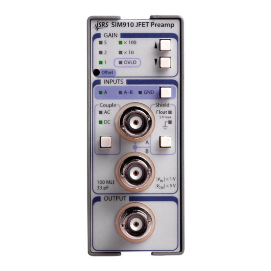
Figure 1.2: The SIM910 front and rear panel. 1.2.1 Gain The gain is selectable from 1 to 100. Gain settings are 1, 2, 5, 10, 20, 50, and 100 and are displayed as a product of 1, 2, or 5 and a multiplier of 10 or 100. -
Page 12: Inputs
BNC connector. Note about grounds The chassis of the SIM910 is tied to the power supply return, and not Signal Ground. When operating in the SIM900, the chassis and Signal Ground are tied together in the SIM900 Mainframe. If the amplifier is operated with an independent supply, the output will be referenced to Signal Ground (pin 1 on DB–15 J401). -
Page 13: Rear Panel Output
The rear panel output is wired in parallel to the front panel output. The output is not designed to drive 2 simultaneous 50 loads. If one output is driving a 50 load, the other should be connected to a high impedance load. SIM910 JFET Preamp... -
Page 14: Sim Interface
SIM900 Mainframe via this connection, either through one of the internal mainframe slots, or the remote cable interface. It is also possible to operate the SIM910 directly, without using the SIM900 Mainframe. This section provides details on the interface. - Page 15 RS-232 serial port of a personal computer. Connect RXD from the SIM910 directly to RD on the PC, TXD directly to TD, and similarly RTS RTS and CTS CTS. In other words, a null-modem style cable is not needed.
- Page 16 1.4.2.2 Serial settings The serial port settings at power-on are: 9600 baud, 8–bits, no parity, 1 stop bit, and hardware flow control (see Section 2.3.1). The serial settings cannot be changed on the SIM910. SIM910 JFET Preamp...
-
Page 17: Remote Operation
2 Remote Operation This chapter describes operating the module over the serial interface. In This Chapter 2.1 Index of Common Commands ... . . 2 – 2 Alphabetic List of Commands ... . . 2 – 3 Introduction . -
Page 18: Index Of Common Commands
2 – 7 Service Request Enable STOL(?) i 2 – 7 Status Monitors Overload OVLD? 2 – 7 Overload Interface *IDN? 2 – 8 Identify 2 – 8 Self Test *TST? CONS(?) i 2 – 8 Console Mode SIM910 JFET Preamp... -
Page 19: Alphabetic List Of Commands
COUP(?) i 2 – 6 Coupling GAIN(?) i 2 – 6 Gain INPT(?) i 2 – 6 Input OVLD? 2 – 7 Overload SHLD(?) i 2 – 6 Shield STOL(?) i 2 – 7 Status Monitors Overload SIM910 JFET Preamp... -
Page 20: Introduction
2 – 4 Remote Operation 2.3 Introduction Remote operation of the SIM910 is through a simple command lan- guage documented in this chapter. Both set and query forms of most commands are supported, allowing the user complete control of the amplifier from a remote computer, either through the SIM900 Main-... -
Page 21: Commands
Each command is provided with a simple example illustrating its usage. In these examples, all data sent by the host computer to the SIM910 are set as straight teletype font, while responses received the host computer from the SIM910 are set as slanted teletype font. SIM910 JFET Preamp... -
Page 22: Amplifier Commands
Example: INPT 2 SHLD(?) i Shield Set (query) the amplifier input BNC shield configuration. SHLD 1 floats the A & B input shields, while SHLD 2 ties the input shields to amplifier ground. Example: SHLD? SIM910 JFET Preamp... -
Page 23: Status Commands
2.4 Commands 2 – 7 2.4.5 Status commands The Status commands query and configure registers associated with status reporting of the SIM910. *STB? Status Byte Reads the Status Byte register. Execution of the *STB? query clears all flag bits set in the Status Byte register (see the Register Model section 2.5 for more about the Status... -
Page 24: Interface Commands
Example: *IDN? Stanford Research Systems,SIM910,s/n003456,ver2.10 *TST? Self Test Query the device self test. The SIM910 does not perform any self tests, and will always return the message 0 to this query. Example: *TST? CONS(?) i Console Mode Set (query) the Console mode to i (0, 1) . -
Page 25: Register Model
2 – 9 2.5 Register Model The SIM910 monitors and reports errors and other conditions using a single 8-bit register, the Status Byte register. Each bit in the register is mapped to a particular event category, and if that event occurs the corresponding bit is set to 1. -
Page 26: Service Request Enable (Sre)
STATUS signal (pin 2 on the Dsub-15 SIM Interface Connector) is asserted low. This register is set and queried with the *SRE(?) command. On Power-On, this register is cleared. SIM910 JFET Preamp... -
Page 27: Performance Tests
Performance Tests ....3 – 3 SIM910 Performance Test Record ... 3 – 4... -
Page 28: Calibration
JFET. Locate R120, the ”CMRR Adjust” trimpot, on the inside of the SIM910. Set the module’s gain to 100, input mode to A B, coupling to DC, and shield to grounded. Generate a 1 V amplitude sine wave at 1 kHz. -
Page 29: Performance Tests
These are noise plots with the input grounded internally. If you are amplifying a small signal far from the SIM900 Mainframe it could be preferable to run the SIM910 on an external supply, i.e. the one which is powering your other electronics. To do this, simply supply 15 V and a signal ground to power the signal electronics and 5V and Power ground to power the microprocessor. -
Page 30: Sim910 Performance Test Record
3 – 4 Performance Tests your signal reference. See table 1.1 for the power and communication connector pin specifications. 3.4 SIM910 Performance Test Record Description Measured Value Serial Number Clock Frequency at TP401 Gain 1 Gain 2 Gain 5 Gain 10... - Page 31 4 Parts Lists and Schematics This chapter presents a brief description of the SIM910 circuit design. A complete parts list and circuit schematics are included. In This Chapter 4.1 Circuit Discussion ....4 – 2 4.1.1...
-
Page 32: Circuitry
U201 and U203 are closed based on gain. The overall gain of the SIM910 is trimmed at U204, the gain of which is adjustable by 10 %. The final output stage rolls the gain o slowly above 1 MHz, and includes a high-current output bu er (U207) ca- pable of driving long coaxial cables and other reactive loads. - Page 33 When the microcontroller has completed all pending activity, it drives the STOP signal high (pin 24 of U405), e ectively halting its own processor clock. In this way, the SIM910 guarantees no digital clock artifacts can be generated during quiescent operation.
-
Page 34: Parts List
U403 3-00742 74HC74 R116,R115 4-01027 U404 3-01405 74AC00 R118,R119 4-01611 8.25 U405 3-01406 68HC705C8A R120 4-00486 50.0 U406 3-01407 93AA56 R122,R121 4-01355 301K U407 3-00662 74HC14 R125 4-01134 1.50K 4.3 Schematic Diagrams Schematic diagrams follow this page. SIM910 JFET Preamp...
Need help?
Do you have a question about the SIM910 and is the answer not in the manual?
Questions and answers