Table of Contents
Advertisement
Quick Links
Advertisement
Table of Contents

Related Manuals for ROHS ITX-i7418VL


Summary of Contents for ROHS ITX-i7418VL
- Page 2 ITX-i7418VL Mini ITX Industrial Motherboard User’s Manual Version 1.0 2007.05...
-
Page 3: Table Of Contents
Index Table of Contents Chapter 1 Introduction ............4 1.1 Copyright Notice ................5 1.2 About this User’s Manual ............5 1.3 Warning ..................5 1.4 Replacing the lithium battery ............6 1.5 Technical Support ...............6 1.6 Warranty ..................7 1.7 Packing List ................8 1.8 Ordering Information ..............8 1.9 Specification ................9 1.10 Board Dimensions ..............10 1.11 Installing the CPU ..............12... - Page 4 Index Chapter 3 BIOS ..............26 3.1 BIOS Introduction ..............27 3.2 BIOS Setup ................27 3.3 Standard CMOS Features ............28 3.4 Advanced BIOS Features ............31 3.5 Advanced Chipset Features .............35 3.6 Integrated Peripherals ..............39 3.7 Power Management Setup ............44 3.8 PNP/PCI Configurations ............47 3.9 PC Health Status ..............49 3.10 Frequency/Voltage Control .............50 3.11 Load Optimized Defaults ............51...
-
Page 5: Chapter 1 Introduction
Introduction Chapter 1 Introduction... -
Page 6: Copyright Notice
Introduction 1.1 Copyright Notice All Rights Reserved. The information in this document is subject to change without prior notice in order to improve the reliability, design and function. It does not represent a commitment on the part of the manufacturer. Under no circumstances will the manufacturer be liable for any direct, indi- rect, special, incidental, or consequential damages arising from the use or in- ability to use the product or documentation, even if advised of the possibility... -
Page 7: Replacing The Lithium Battery
Introduction 1.4 Replacing the lithium battery Incorrect replacement of the lithium battery may lead to a risk of explosion. The lithium battery must be replaced with an identical battery or a battery type recommended by the manufacturer. Do not throw lithium batteries into the trashcan. It must be disposed of in accordance with local requlations concerning special waste. -
Page 8: Warranty
Introduction 1.6 Warranty This product is warranted to be in good working order for a period of two years from the date of purchase. Should this product fail to be in good working order at any time during this period, we will, at our option, replace or repair it at no additional charge except as set forth in the following terms. -
Page 9: Packing List
Introduction 1.7 Packing List 1x ITX-i7418VL Mini ITX Industrial MB 1x I/O Bracket 1x CPU Heat Sink or Cooler or or 1x CD-ROM (For Driver used) 1x Quick Installation Guide 1x Warranty Card If any of the above items is damaged or missing, contact your vendor immediately. -
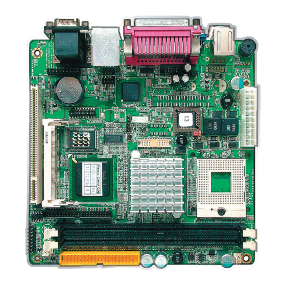
Page 10: Specification
Introduction 1.9 Specification Product Name ITX-i7418VL Form Factor Mini ITX Industrial MB (170 x 170 mm) Processor μFC-PGA478 pin Pentium-M Up to 1.8GHz FSB 400MHz μFC-BGA479 pin Celeron-M 600MHz or 1GHz FSB 400MHz (Optional) Chipset Intel 852GM + Intel ICH4... -
Page 11: Board Dimensions
Introduction 1.10 Board Dimensions... - Page 12 Introduction...
-
Page 13: Installing The Cpu
Introduction 1.11 Installing the CPU The processor socket comes with a screw to secure the CPU. As showing in the picture as below, loose the screw first before inserting the CPU. Place the CPU into the socket by making sure the notch on the corner of the CPU corresponding with the notch on the inside of the socket. -
Page 14: Installing The Memory
Introduction 1.12 Installing the Memory To install the Memory module, locate the Memory DIMM slot on the board and perform as below: 1. Hold the Memory module so that the key of the Memory module align with those on the Memory DIMM slot. 2. -
Page 15: Chapter 2 Installation
Installation Chapter 2 Installation... -
Page 16: Jumpers And Connectors
Installation 2.1 Jumpers and Connectors... -
Page 17: Atx: Atx Power Supply Connector
Installation 2.2 ATX: ATX Power Supply Connector Description Description 3.3V 3.3V -12V 3.3V PS-ON PW-OK 5VSB +12V 2.3 JVLCD1: LCD Panel Voltage Selection The voltage of LCD panel could be selected by JVLCD1 in 5V or 3.3V. Voltage 3.3V (Default) -
Page 18: Lvds1: Lvds Lcd Connector
Installation 2.4 LVDS1: LVDS LCD Connector The LVDS connector on board DF-13 30-pin header and supports 18-bit or 36-bit. Description Description TX2CLK+ TX1CLK+ TX2CLK- TX1CLK- TX2D0+ TX1D0+ TX2D0- TX1D0- TX2D1+ TX1D1+ TX2D1- TX1D1- TX2D2+ TX1D2+ TX2D2- TX1D2- TX2D3+ TX1D3+ TX2D3- TX1D3- 2.5 CPUF1: CPU Fan Power Connector CPUF1 is a 3-pin header for the CPU fan. -
Page 19: Sysf1: System Fan Power Connector
Installation 2.6 SYSF1: System Fan Power Connector SYSF1 is a 3-pin header for the CPU fan. The fan must be a 12V fan. Description +12V FAN_CTL 2.7 IDE2: Secondly 44-pin IDE Connector Description Description IDE RESET DATA7 DATA8 DATA6 DATA9 DATA5 DATA10 DATA4... -
Page 20: Ide1: Primary 40-Pin Ide Connector
Installation 2.8 IDE1: Primary 40-pin IDE Connector 2.9 JFRT1: Switches and Indicators It provides connectors for system indicators that provides light indication of the computer activities and switches to change the computer status. Description Description Power LED+ PWRBTN+ PWRBTN- RESET+ HDD LED+ RESET- HDD LED-... -
Page 21: Jbat1: Cmos Setup
Installation 2.12 JBAT1: CMOS Setup Voltage Keep CMOS (Default) Clear CMOS 2.13 FDD1: FDD Connector FDD1 is a 26-pin connector. Description Description Drive density select 0 N/C (Key) Drive density select 1 #Write data #Index #Write gate #Motor enable A #Track 0 #Driver select B #Write protect 14... -
Page 22: Inv1: Lcd Inverter Connector
Installation 2.15 INV1: LCD Inverter Connector Onboard 5-pin mini boxheader Voltage +12V Backlight on/off Brightness control 2.16 DIO1: Digital I/O Connector DIO1 is a 16 bit GPIO connector w/ Onboard 20-pin 2.54 mm pin header connector Description Description DIO0 DIO1 DIO2 DIO3 DIO4... -
Page 23: Com1: Two D-Sub 9 Connector
Installation 2.17 COM1: Two D-SUB 9 Connector COM1-A Description Description COM1-B 2.18 USB5: USB Connector USB5 supports 2 USB 2.0 w/ 480MB/s Description Description USBD- USBD- USBD+ USBD+ 2.19 CN2: 10/100 RJ-45 + USB1 + USB2 CN2 supports one 10/100 Mbps Fast Ethernet (Intel 82562EZ PHY) and two USB 2.0 connectors w/ 480MB/s. -
Page 24: Audio1: Audio Interface Port
Installation 2.20 AUDIO1: Audio Interface Port AUDIO1 is composed of Line in, Line out and Microphone jacks. Description Description Line Left in Line Right in Speaker LEFT Speaker Right 2.21 USB3/ USB4 USB3/ USB4 connector supports USB 2.0 w/ 480MB/s. USB3 USB4 2.22 LPT1: Parallel Port Connector... -
Page 25: Vga1: Crt Connector
Installation 2.23 VGA1: CRT Connector VGA1 2.24 KBM1: PS/2 Keyboard & Mouse Mouse Keyboard... - Page 26 Installation This page is intentionally left blank.
-
Page 27: Chapter 3 Bios
BIOS Chapter 3 BIOS... -
Page 28: Bios Introduction
BIOS 3.1 BIOS Introduction The Award BIOS (Basic Input/Output System) installed in your computer sys- tem’s. The BIOS provides for a standard device such as disk drives, serial ports and parallel ports. It also adds password protection as well as special support for detailed fine-tuning of the chipset controlling the entire system. -
Page 29: Standard Cmos Features
BIOS 3.3 Standard CMOS Features “Standard CMOS Features” allows you to record some basic hardware configurations in your computer system and set the system clock and error handling. If the CPU card is already installed in a working system, you will not need to select this option. - Page 30 BIOS IDE Primary HDDs / IDE Secondary HDDs The onboard PCI IDE connectors provide Primary and Secondary channels for connecting up to four IDE hard disks or other IDE devices. Each channel can support up to two hard disks; the first is the “Master” and the second is the “Slave”.
- Page 31 BIOS Halt On This field determines whether or not the system will halt if an error is detected during power up. All errors Whenever the BIOS detects a non-fatal error, the system will stop and you will be prompted. No errors The system boot will not be halted for any error that may be detected.
-
Page 32: Advanced Bios Features
BIOS 3.4 Advanced BIOS Features CPU L1/ L2/ L3 Cache Cache memory is additional memory that is faster than conventional DRAM (system memory). CPUs from 486-type on up contain internal cache memory, and most, but not all, modern PCs have additional (external) cache memory. When the CPU requests data, the system transfers the requested data from the main DRAM into cache memory, for even faster access by the CPU. -
Page 33: Boot Other Device
BIOS First/ Second/ Third Boot Device These fields determine the drive that the system searches first for an operating system. The options available include Setting: Floppy, LS120, HDD-0, SCSI, CDROM, HDD-1, HDD-2, HDD-3, ZIP100, USB-FDD, USB-ZIP, USB-CDROM, USB-HDD, LAN and Disabled. -
Page 34: Typematic Rate Setting
BIOS Gate A20 Option It allows you to select how the Gate A20 is worked. Gate A20 is a device used to address memory above 1 MB. Setting: Normal, Fast (Default). Typematic Rate Setting When disabled, continually holding down a key on your keyboard will generate only one instance. -
Page 35: Mps Version Control For Os
BIOS MPS Version Control for OS It is specifies the MPS (Multiprocessor Specification) version for your operating system. MPS version 1.4 added extended configuration tables to improve support for multiple PCI bus configurations and improve future expandability. Setting: 1.1, 1.4 (Default). Small Logo (EPA) Show The EPA logo appears at the right side of the monitor screen when the system is boot up. -
Page 36: Advanced Chipset Features
BIOS 3.5 Advanced Chipset Features DRAM Timing Selectable It refers to the method by which the DRAM timing is selected. Setting: Manual, By SPD (Default). CAS Latency Time It allows CAS latency time in HCLKs as 2 or 2.5. The system board designer should set the values in this field, depending on the DRAM installed. -
Page 37: System Bios Cacheable
BIOS DRAM RAS# to CAS# Delay It allows you to insert a delay between the RAS (Row Address Strobe) and CAS (Column Address Strobe) signals. This delay occurs when the SDRAM is written to, read from or refreshed. Reducing the delay improves the performance of the SDRAM. -
Page 38: Delayed Transaction
BIOS Memory Hole At 15M-16M In order to improve performance, certain space in memory can be reserved for ISA cards. This memory must be mapped into the memory space below 16 MB. Setting: Disabled (Default), Enabled. Delayed Transaction The chipset has an embedded 32-bit posted write buffer to support delay transactions cycles. - Page 39 BIOS Boot Display Setting: VBIOS Default, CRT (Default), LFP, CRT+LFP, EFP, TV, CRT+EFP, CRT+TV. Panel Number It allows you to select the LCD Panel type as below --- Setting: 640x480 18-bit 800x600 18-bit 1024x768 18-bit (Default) 1280x1024 18-bit 1400x1050 18-bit 2-CH 1600x1200 18-bit...
-
Page 40: Integrated Peripherals
BIOS 3.6 Integrated Peripherals OnChip Primary/Secondary PCI IDE The integrated peripheral controller contains an IDE interface with support for two IDE channels. Select Enabled to activate each channel separately. Setting: Disabled, Enabled (Default). -
Page 41: Usb Controller
BIOS IDE Primary/Secondary Master/Slave PIO It allows your system HDD controller to run faster. Rather than having the BIOS issue with a series of commands that transferring to or from the disk drive, PIO (Programmed Input/Output) allows the BIOS to communicate with the controller and CPU directly. When Auto is selected, the BIOS will select the best available mode. -
Page 42: Ac97 Audio
BIOS USB Keyboard/ Mouse Support For using USB 2.0, it is necessary OS drivers must be installed first. Please update your system to at least Windows 2000 SP4 or Windows XP SP2. Setting: Disabled, Enabled (Default). AC97 Audio Setting: Auto (Default), Disabled. Init Display First This determines which VGA controller is initialized when the system boots. - Page 43 BIOS Onboard Serial/Parallel Port It allows you to select the onboard serial and parallel ports with their addresses. Setting: Serial Port 1 3F8/IRQ4 (Default) Serial Port 2 2F8/IRQ3 (Default) Parallel Port 378H/IRQ7 (Default) UART Mode Select It determines the UART 2 mode in your computer. Setting: IrDA, ASKIR, Normal (Default).
- Page 44 BIOS EPP Mode Select Setting: EPP1.9, EPP1.7 (Default) ECP Mode Use DMA Setting: 1, 3 (Default). PWRON After PWR-Fail It sets the system power status whether on or off when power returns to the system from a power failure situation. Setting: Off (Default), On, Former-Sts.
-
Page 45: Power Management Setup
BIOS 3.7 Power Management Setup ACPI Function It supports ACPI (Advance Configuration and Power Interface). Setting: Enabled (Default), Disabled. Power Management It allows you to select the type of power saving management modes. Setting: User Define (Default) Each of the ranges is from 1 min. to 1hr. Except for HDD Power Down which ranges from 1 min. -
Page 46: Video Off In Suspend
BIOS Video Off In Suspend When enabled, the video is off in suspend mode. Setting: No, Yes (Default). Suspend Type Setting: Stop Grant (Default), PwrOn Suspend. Modem Use IRQ It sets the IRQ used by the Modem. Setting: NA (Default), 3, 4, 5, 7, 9, 10, 11. Suspend Mode When “Enabled”, after the set time of system inactivity, all devices except the CPU will be shut off as the set time. -
Page 47: Resume By Alarm
BIOS Power-On by LAN/ Ring It enables or disables the power on of the system through the modem connected or LAN. Setting: Disabled (Default), Enabled. Resume by Alarm It enables or disables the resumption of the system operation. When enabled, the user is allowed to set the Date and Time. Setting: Disabled (Default), Enabled. -
Page 48: Resources Controlled By
BIOS 3.8 PNP/PCI Configurations Reset Configuration Data It allows you to determine whether to reset the configuration data or not. Setting: Disabled (Default), Enabled. Resources Controlled By This PnP BIOS can configure all of the boot and compatible devices with the use of a PnP operating system. - Page 49 BIOS PCI/VGA Palette Snoop Some non-standard VGA display cards may not show colors properly. It allows you to set whether or not MPEG ISA/VESA VGA cards can display with PCI/VGA. When “Enabled”, a PCI/VGA can display with an MPEG ISA/VESA VGA card.
-
Page 50: Pc Health Status
BIOS 3.9 PC Health Status Shutdown Temperature It allows you to set the temperature by which the system automatically shuts down once the threshold temperature is reached. The setting can help prevent damage to the system that is caused by overheating. -
Page 51: Frequency/Voltage Control
BIOS 3.10 Frequency/Voltage Control Auto Detect PCI Clk It enables or disables the auto detection of the PCI clock. Setting: Enabled (Default), Disabled. Spread Spectrum It sets the value of the spread spectrum. It is for CE testing use only. Setting: Disabled (Default), Enabled. -
Page 52: Load Optimized Defaults
BIOS 3.11 Load Optimized Defaults It allows you to load the default values to your system configuration. The default setting is optimal and enabled all high performance features. -
Page 53: Set Password
BIOS 3.12 Set Password Useing Password to set a password that will be used exclusively on the system. To specify a password, highlight the type you want and press <Enter>. The Enter Password: message prompts on the screen. Type the password, up to eight characters in length, and press <Enter>. -
Page 54: Save & Exit Setup
BIOS 3.13 Save & Exit Setup Typing “Y”, you will quit the setup utility and save all the changes into the CMOS memory. Typing “N”, you will return to Setup utility. -
Page 55: Exit Without Saving
BIOS 3.14 Exit Without Saving Typing “Y” will quit the Setup utility without saving the modifications. Typing “N” will return you to Setup utility. -
Page 56: Bios Beep Sound Code List
BIOS 3.15 BIOS Beep Sound code list Beep Sound Message 1 short (Beep) System booting is normally 2 short (Beep) CMOS setting error 1 long - 1 short (Beep) DRAM error 1 long - 2 short (Beep) Display card or monitor connected error 1 long - 3 short (Beep) Keyboard error 1 long - 9 short (Beep) -
Page 57: Award Bios Post Codes
3.17 Award BIOS Post Codes CFh Test CMOS read/write functionality Early chipset initialization: Disable shadow RAM, L2 cache (socket 7 and below), program basic chipset registers C1h Detect memory: Auto detection of DRAM size, type and ECC, auto detection of L2 cache (socket 7 and below) C3h Expand compressed BIOS code to DRAM C5h Call chipset hook to copy BIOS back to E000 &... - Page 58 Reserved HPM initialization (notebook platform) Reserved Check validity of RTC value; Load CMOS settings into BIOS stack. If CMOS checksum fails, use default value instead; Prepare BIOS resource map for PCI & PnP use. If ESCD is valid, take into consideration of the ESCD's legacy information;...
- Page 59 Initialize EISA slot Reserved Calculate total memory by testing the last double last word of each 64K page; Program writes allocation for AMD K5 CPU Reserved Reserved 4Ch Reserved 4Dh Reserved Program MTRR of M1 CPU; initialize L2 cache for P6 class CPU & program cacheable range;...
- Page 60 Reserved Reserved Reserved Enter AWDFLASH.EXE if: AWDFLASH.EXE is found in floppy dive and ALT+F2 is pressed Reserved Detect and install all IDE devices: HDD, LS120, ZIP, CDROM... Reserved Detect serial ports and parallel ports Reserved Reserved Detect and install coprocessor Reserved 7Ch Reserved 7Dh Reserved...
-
Page 61: Chapter 4 Appendix
Appendix Chapter 4 Appendix... -
Page 62: I/O Port Address Map
Appendix 4.1 I/O Port Address Map Each peripheral device in the system is assigned a set of I/O port addresses which also becomes the identity of the device. The following table lists the I/O port addresses used. Address Device Description 000h - 01Fh DMA Controller #1 020h - 03Fh... -
Page 63: Interrupt Request Lines (Irq)
Appendix 4.2 Interrupt Request Lines (IRQ) Peripheral devices use interrupt request lines to notify CPU for the service required. The following table shows the IRQ used by the devices on board. Level Function IRQ 0 System Timer IRQ 1 Keyboard IRQ 2 Cascaded with IRQ 9 IRQ 3... - Page 64 Appendix This page is intentionally left blank.
Need help?
Do you have a question about the ITX-i7418VL and is the answer not in the manual?
Questions and answers