Table of Contents
Advertisement
Specifications
Main unit SA-BT100P/PC
GENERAL
Power supply:
iPod connector:
Power consumption:
Power consumption in standby mode:
Dimensions (W×H×D):
With transmitter:
Without transmitter:
Mass:
Operating temperature range:
Operating humidity range:
AMPLIFIER SECTION
RMS TTL Output Power:
Front Ch:
Blu-ray Disc Home Theater Sound System
AC 120 V, 60 Hz
DC OUT 5V 500 mA MAX
This unit 140 W
approx. 0.3 W
430 mmx96 mmx327 mm
(16-15/16" X 3-25/32" X 12-7/8")
430 mmx90 mmx327 mm
(16-15/16" X 3-9/16" X 12-7/8")
This unit approx 4.1 kg(9.1 lbs)
+0 °C to +40 °C
(+32 °F to +104 °F)
35 % to 80 % RH
(no condensation)
SA-BT100P
SA-BT100PC
Colour
(K).......................Black Type
250 W per channel (6 Ω), 1 kHz, 10% THD
Surround Ch:
125 W per channel (3 Ω), 1 kHz, 10% THD
Center Ch:
250 W per channel (6 Ω), 1 kHz, 10% THD
Subwoofer Ch:
250 W per channel (6 Ω), 100 Hz, 10 % THD
Total RMS TTL power:
FTC TTL Output Power:
Front Ch:
104 W per channel (6 Ω), 120Hz to 20 kHz, 1.0% THD
Surround Ch:
34 W per channel (3 Ω), 120Hz to 20 kHz, 1.0% THD
Center Ch:
101 W per channel (6 Ω), 120Hz to 20 kHz, 1.0% THD
Subwoofer Ch:
95 W per channel (6 Ω), 45 Hz to120 Hz, 1.0% THD
Total FTC TTL power:
Audio Input:
© 2008 Matsushita Electric Industrial Co. Ltd.. All
rights
reserved.
distribution is a violation of law.
ORDER NO. MD0803025CE
1250 W
472 W
Unauthorized
copying
and
A6
Advertisement
Table of Contents

Related Manuals for Panasonic SA-BT100P


Summary of Contents for Panasonic SA-BT100P
-
Page 1: Specifications
SA-BT100P SA-BT100PC Colour (K).......Black Type Specifications 250 W per channel (6 Ω), 1 kHz, 10% THD Main unit SA-BT100P/PC GENERAL Surround Ch: 125 W per channel (3 Ω), 1 kHz, 10% THD Power supply: AC 120 V, 60 Hz iPod connector:... -
Page 2: Includes Sdhc Card
SA-BT100P / SA-BT100PC AUX: The total combined maximum number of recognizable picture contents and folders: 9999 picture contents and 300 folders. AVCHD format V1.0 Digital Audio Input: VIDEO SECTION Optical: Signal system: NTSC Video output FM TUNER SECTION 1.0 Vp-p (75 Ω) - Page 3 SA-BT100P / SA-BT100PC CONTENTS Page Page 1 Safety Precautions 1.3. Protection Circuitry 1.1. GENERAL GUIDELINES 1.4. Safety Parts Information 1.2. Before Repair and Adjustment...
-
Page 4: Table Of Contents
SA-BT100P / SA-BT100PC 2 Prevention of Electrostatic Discharge (ESD) to 12.3. Checking & Repairing SMPS P.C.B. Electrostatically Sensitive (ES) Devices 12.4. Checking & Repairing DSP P.C.B. 3 Precaution of Laser Diode 12.5. Checking & Repairing Digital P.C.B. 4 About Lead Free Solder (PbF) 13 Caution for Replacing Parts 4.1. - Page 5 SA-BT100P / SA-BT100PC 22.2. IC6001(C0HBB0000057): IC FL Driver 24 Replacement Parts List 23 Exploded Views 24.1. Component Parts List 23.1. Cabinet Parts Location 25 Schematic Diagram for printing with letter size 23.2. Packaging...
-
Page 6: Before Repair And Adjustment
SA-BT100P / SA-BT100PC 1 Safety Precautions 1.1. GENERAL GUIDELINES 1. When servicing, observe the original lead dress. If a short circuit is found, replace all parts which have been overheated or damaged by the short circuit. 2. After servicing, see to it that all the protective devices such as insulation barriers, insulation papers shields are properly installed. -
Page 7: Protection Circuitry
SA-BT100P / SA-BT100PC 1.2.1. Caution for fuse replacement 1.3. Protection Circuitry The protection circuitry may have operated if either of the following conditions are noticed: • • • • No sound is heard when the power is turned on. • • • • Sound stops during a performance. - Page 8 SA-BT100P / SA-BT100PC Ref. No. Part No. Part Name & Description Remarks PC5702 B3PBA0000402 PHOTO COUPLER PC5720 B3PBA0000402 PHOTO COUPLER PC5799 B3PBA0000402 PHOTO COUPLER K5D802APA008 FUSE IP7001 K5H7512A0010 PROTECTOR IP58301 ERBSE3R00U PROTECTOR TH5701 D4CAA2R20001 THERMISTOR TH5860 D4CC11040013 THERMISTOR P5701 K2AB2B000010...
-
Page 9: Prevention Of Electrostatic Discharge (Esd) To
SA-BT100P / SA-BT100PC 2 Prevention of Electrostatic Discharge (ESD) to Electrostatically Sensitive (ES) Devices Some semiconductor (solid state) devices can be damaged easily by static electricity. Such components commonly are called Electrostatically Sensitive (ES) Devices. Examples of typical ES devices are integrated circuits and some field-effect transistors and semiconductor "chip"... -
Page 10: Precaution Of Laser Diode
SA-BT100P / SA-BT100PC 3 Precaution of Laser Diode CAUTION : This product utilizes a laser diode with the unit turned "on", invisible laser radiation is emitted from the pickup lens. Wavelength: 662 nm (DVD)/782 nm (CD)/405 nm (BD) Maximum output radiation power from pickup: 100 µW/VDE Laser radiation from the pickup unit is safety level, but be sure the followings: 1. -
Page 11: About Lead Free Solder (Pbf)
SA-BT100P / SA-BT100PC 4 About Lead Free Solder (PbF) 4.1. Service caution based on legal restrictions 4.1.1. General description about Lead Free Solder (PbF) The lead free solder has been used in the mounting process of all electrical components on the printed circuit boards used for this equipment in considering the globally environmental conservation. -
Page 12: Service Navigation
SA-BT100P / SA-BT100PC 5 Service Navigation 5.1. Service Information The service manual contains technical information which will allow service personnel’s to understand and service this model. Please place orders using the parts list and not the drawing reference numbers. If the circuit is changed or modified, the information will be followed by supplement service manual to be filed with original service manual. -
Page 13: Accessories
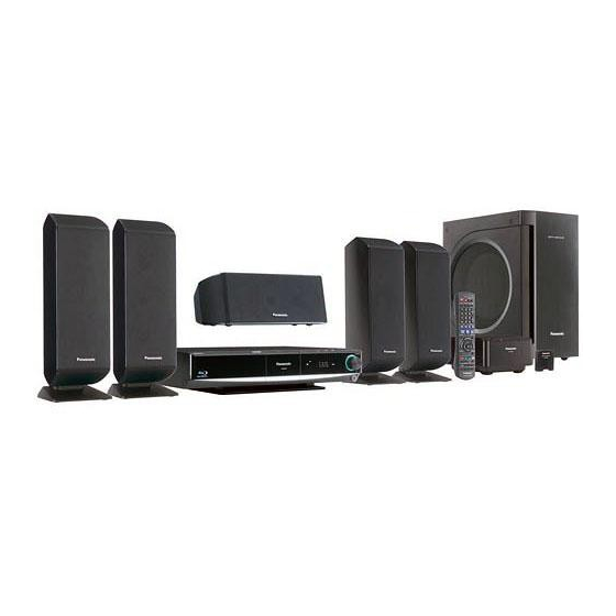
SA-BT100P / SA-BT100PC 6 Accessories • • • • Note: Refer to “Replacement Parts List” (Section 25) for the part number. AM loop antenna Remote control AC cord FM Indoor Antenna (For SA-BT100 & SH-FX67) Speaker cable sticker Video cable... -
Page 14: Operation Procedures
Select speaker channel [MUTING]: Mute the sound Transmit the remote control signal TV operation buttons Aim the remote control at the Panasonic TV and press the button. TV]: Turn the TV on and off [TV/VIDEO]: Switch the input channel VOL]: Adjust the TV volume This may not work properly with some models. -
Page 15: Main Unit Key Buttons Operations
SA-BT100P / SA-BT100PC 7.2. Main Unit Key Buttons Operations Main unit 4 5 6 7.1CH BOOST D.S.P. SELECTOR Place your finger on the section and open it diagonally downwards. POWER button (POWER Select the radio station manually Press to switch the unit form on to standby mode vice versa. In Search /Slow-motion/Skip standby mode, the unit is still consuming a small amount of power. -
Page 16: What Is Viera Link Hdavi Control
VIERA Link HDAVI Control , based on the control VIERA Link HDAVI Control is a convenient function that offers linked functions provided by HDMI which is an industry operations of this unit, and a Panasonic TV (VIERA) under HDAVI standard known as HDMI CEC (Consumer NOTE Control . -
Page 17: Using The Ipod
Audio/video cannot be recorded or transmitted to NOTE iPods via this system. iPod nano 3rd generation (video) 4 GB, 8 GB Panasonic makes no warranty over iPod data iPod classic 80 GB, 160 GB management. iPod nano 2nd generation (aluminum) - Page 18 SA-BT100P / SA-BT100PC Playback This system features two different iPod playback modes. The first of these is EXTENDED mode, for playback of music contents. With this mode, the menu screen on the system can be used to search for playlists and artist names, and to play music. The second mode is SIMPLE mode, which can be used for playback of three types of contents music, photos, and videos.
-
Page 19: Playing Secondary Video And Audio
SA-BT100P / SA-BT100PC 7.5. Playing Secondary Video and Audio Playing secondary video (picture-in-picture) and secondary audio Secondary video can be played from a disc compatible with the picture-in-picture Only the primary video is played during search/ function. slow-motion or frame-by-frame. -
Page 20: Basic Connections
SA-BT100P / SA-BT100PC 7.6. Basic Connections 7.6.1. Speaker Cables and Transmitter Connection Do not place the unit on amplifiers or equipment that may become hot. The heat can damage the unit. Turn off all equipment before connection and read the appropriate operating instructions. -
Page 21: Connection To A Tv
SUBWOOFER CENTER Please use High Speed HDMI cables that have the HDMI logo (as shown on the cover). It is recommended that you use Panasonic’s HDMI cable. Recommended part number: NOTE RP-CDHG10 (1.0 m/3.3 ft.), RP-CDHG15 (1.5 m/4.9 ft.), RP-CDHG20 (2.0 m/6.6 ft.), RP-CDHG30 (3.0 m/9.8 ft.), PR-CDHG50 (5.0 m/16.4 ft.), etc. -
Page 22: Radio Antenna Connections
SA-BT100P / SA-BT100PC 7.6.3. Radio Antenna and AC Power Supply Cord Connections Radio antenna connections FM Indoor antenna AM loop antenna AM loop antenna (included) FM indoor antenna (included) Stand the antenna up on its base. Affix this end of the antenna where Place the antenna where reception reception is best. -
Page 23: Disc And Sd Cards Information
SA-BT100P / SA-BT100PC 7.6.4. Setting up the unit Turn on the main unit and wireless system Turn on the power of the main unit and the wireless system after all connections are complete. Preparation AUTO OPERATION ON/OFF Turn on the TV and select the appropriate video input on the TV. -
Page 24: Recorded Discs
7.7.3. SD Cards This chart shows the different type of cards recorded with Panasonic High Definition Video Camera or personal computers, etc. that you can use. Type of media Features Indicated as... -
Page 25: Discs That Cannot Be Played
SA-BT100P / SA-BT100PC 7.7.5. Note about using a DualDisc The digital audio content side of DualDisc does not meet the technical specifications of the Compact Disc Digital Audio (CD-DA) format so play may not be possible. 7.7.6. Tips for making MP3/JPEG Discs... -
Page 26: Operation Instructions
SA-BT100P / SA-BT100PC 8 Operation Instructions 8.1. Taking out the Disc from BD/DVD Drive Unit when Disc cannot be ejected by OPEN/CLOSE button 8.1.1. Forcible Disc Eject 8.1.1.1. When the power can be turned off. 1. Turn off the power and press [SKIP REV] and [PLAY] keys on the front panel simultaneously for 5 seconds. -
Page 27: Service Mode
SA-BT100P / SA-BT100PC 9 Service Mode 9.1. Self-Diagnosis and Special Mode Setting Self-Diagnosis Function provides information for error to service personnel by Self-Diagnosis Display when any error has occurred. U**, H** and F** are stored in my memory and held. - Page 28 SA-BT100P / SA-BT100PC 9.1.1. Error Code Table 1 Error Code Diagnosis contents Description Monitor Display Automatic FL display Remote control code error Display appears when main unit and remote No display controller codes are not matched. is remote controller code of the main unit.
- Page 29 SA-BT100P / SA-BT100PC 9.1.2. Error Code Table 2 Error Code Diagnosis contents Description Monitor Display Automatic FL display IR ERR IR communication error [IR ERR] is displayed when communication No display between Timer microprocessor and IR micro- processor fails. SELF...
-
Page 30: Special Mode Setting
SA-BT100P / SA-BT100PC 9.2. Special Mode Setting 9.2.1. Service Mode Table 1 Item FL display Key operation Mode name Description Front Key Initialize Mode *All the main unit’s parameters are initialized. Press [STOP], [SKIP FWD] and [OPEN/CLOSE] keys simulta- INITIALIZE neously for five seconds when power is off. -
Page 31: Service Mode Table
SA-BT100P / SA-BT100PC 9.2.2. Service Mode Table 2 Item FL display Key operation Mode name Description Front Key Demonstration lock/ Ejection of the disc is prohibited. *When lock the tray. When the power is on , unlock The lock setting is effective until unlocking the... -
Page 32: Service Mode At Glance
SA-BT100P / SA-BT100PC 9.3. Service Mode at glance Service mode setting: While the power is off, press [SKIP FWD], [PLAY] and [OPEN / CLOSE] simultaneously for five second. 9.3.1. Service Mode Table 1 Item FL display Key operation Mode name... - Page 33 SA-BT100P / SA-BT100PC 9.3.2. Service Mode Table 2 Item FL display Key operation Mode name Description (Remote controller key) Laser Used Time Check laser used time (hours) of drive. Press [4] [1] in service mode. Indication ****** (******) is the used time display in hour.
- Page 34 SA-BT100P / SA-BT100PC 9.3.3. Service Mode Table 3 Item FL display Key operation Mode name Description (Remote controller key) BD/DVD drive last error BD/DVD drive error code display. 1. Error Number is displayed for 5 Press [4] [2] in service mode.
- Page 35 SA-BT100P / SA-BT100PC 9.3.4. Service Mode Table 4 Item FL display Key operation Mode name Description (Remote controller key) In case that the maker cannot be 6. Disc maker ID is displayed for 5 identified, display is black out. seconds.
- Page 36 SA-BT100P / SA-BT100PC 9.3.5. Service Mode Table 5 Item FL display Key operation Mode name Description (Remote controller key) CEC (H) output Check of the CEC terminal high output of Press [5] [5] in service mode. HDMI. CECHOK CECHNG CEC (L) output Check of the CEC terminal low output of Press [5] [6] in service mode.
-
Page 37: Service Mode Table (Wireless - E.g. Sh-Fx67)
SA-BT100P / SA-BT100PC 9.4. Service Mode Table (Wireless - e.g. SH-FX67) By pressing various button combinations on the player and remote control unit, you can activate the various service modes for checking. 9.4.1. Service Mode Table 1 Item Key Operation... - Page 38 SA-BT100P / SA-BT100PC 9.4.2. Service Mode Table 2 Item Key Operation FL Display Mode Name Description Front Key (Display 1) RF Channel RF Channel 1 Display* Main set is in AUX mode. Selection Display FL Display sequence: Display 1 (Display 2)
-
Page 39: Assembling And Disassembling
SA-BT100P / SA-BT100PC 10 Assembling and Disassembling “ATTENTION SERVICER” Be careful when disassembling and servicing. Some chassis components may have sharp edges. Special Note: 1. This section describes the disassembly procedures for all the major printed circuit boards and main components. - Page 40 SA-BT100P / SA-BT100PC...
-
Page 41: Disassembly Flow Chart
SA-BT100P / SA-BT100PC 10.1. Disassembly Flow Chart 9.3. Top Cabinet 9.4. Rear Panel 9.11. AC Inlet P.C.B. 9.12. Main P.C.B. 9.13. D-Amp P.C.B. 9.14. Digital Amp IC 9.5. Front Panel (IC5000) 9.7. Panel/Headphone/ 9.6. BD/DVD Drive Power Button/Open/Close Unit P.C.B. -
Page 42: Main Components And P.c.b. Locations
SA-BT100P / SA-BT100PC 10.2. Main Components and P.C.B. Locations... -
Page 43: Disassembly Of Top Cabinet
SA-BT100P / SA-BT100PC 10.3. Disassembly of Top Cabinet Step 1 Remove 4 screws at the side of the top cabinet. Step 2 Remove 3 screws at the rear of the top cabinet. Step 4 Remove the wire clamper to detach the fan unit connector (CN5501) on D-Amp P.C.B. -
Page 44: Disassembly Of Bd/Dvd Drive Unit
SA-BT100P / SA-BT100PC DVD Module P.C.B. Step 4 Release the hook at left & right side of the front panel in the direction of arrow. Caution: Do not attempt to exert strong force when detaching the front panel. 10.6. Disassembly of BD/DVD Drive... -
Page 45: Disassembly Of Panel/ Headphone/ Power / Open/Close
SA-BT100P / SA-BT100PC Step 3 Remove 4 screws from BD/DVD Drive unit. Step 4 Remove Mecha shield plate unit. Step 5 Lift the BD/DVD Drive unit in the direction of arrow. Step 2 Remove 3 screws at panel shield. Step 3 Remove panel shield. -
Page 46: Disassembly Of Sd P.c.b
SA-BT100P / SA-BT100PC Caution: Keep the Panel earth spring in safe place. Avoid denting it. Place it back during assembling. 10.8. Disassembly of SD P.C.B. • • • • Follow (Step 1) to (Step 3) of Item 10.3. Step 1 Remove 1 screw at SD earth spring. -
Page 47: Disassembly Of Ipod Cradle
SA-BT100P / SA-BT100PC of arrow. Step 4 Remove the connector cover. Step 5 Use a flat head screwdriver (0.5-0.7mm) to release the catches according to the diagram show. Step 6 Remove cradle cover A as the direction of arrow. 10.10. Disassembly of Ipod Cradle P.C.B. -
Page 48: Disassembly Of Ac Inlet P.c.b
SA-BT100P / SA-BT100PC Step 8 Remove 2 screws on the Ipod cradle P.C.B. Step 2 Remove 2 screws from the AC Inlet shield plate unit. Step 9 Remove Ipod cradle P.C.B. Step 3 Remove the AC Inlet shield plate unit. -
Page 49: Disassembly Of Main P.c.b
SA-BT100P / SA-BT100PC Step 3 Detach 19P FFC cable at the connector (CN802) on the Main P.C.B. Step 4 Detach 24P FFC cable at the connector (CN501) on the Main P.C.B. Step 5 Detach 20P FFC cable at the connector (CN502) on the Main P.C.B. -
Page 50: Disassembly Of D-Amp
SA-BT100P / SA-BT100PC Step 5 Twist the wire clamper to detach 3P cable at the connector (CN5501) on D-Amp P.C.B. Special Note: During reassembling procedures, ensure the P.C.B. is seated properly at the locators. Step 6 Remove 2 screws at the rear panel. -
Page 51: Replacement Of Digital Amp Ic (Ic5000)
SA-BT100P / SA-BT100PC 10.14. Replacement of Digital Amp IC Special Note : For replacement of IC5200, IC5300 & IC5400, (IC5000) repeat the (Step 1) to (Step 4). Refer to the diagrams of D-Amp P.C.B. (Item 20.6) for location of the parts. -
Page 52: Replacement Of Switch Regulator Ic (Ic5701)
SA-BT100P / SA-BT100PC Step 2 Remove 1 screw from the switch regulator IC (IC5701). Step 3 Remove the switch regulator IC (IC5701) from the heatsink unit B. Caution: Handle the heatsink unit B with caution due to its high temperature after prolonged use. Touching it may lead to injuries. -
Page 53: Replacement Of Switch Regulator Diode (D5702)
SA-BT100P / SA-BT100PC Step 3 Solder pins of the switch regulator IC (IC5701) on the reverse side of SMPS P.C.B. Step 3 Remove 1 screw from the switch regulator IC (IC5701). Step 4 Remove the heatsink unit B in the direction of arrows. -
Page 54: Replacement Of Regulator Diode (D5801)
SA-BT100P / SA-BT100PC heatsink unit B. 10.18. Replacement of Regulator Special Note: Ensure the switch regulator diode (D5702) is Diode (D5801) tightly screwed to the heatsink unit B. • • • • Follow (Step 1) to (Step 3) of Item 10.3. -
Page 55: Replacement Of Regulator Diode (D5802)
SA-BT100P / SA-BT100PC Step 3 Remove the regulator diode (D5802) from the heatsink unit C. Caution: Handle the heatsink unit C with caution due to its high temperature after prolonged use. Touching it may lead to injuries. Step 3 Solder pins of the regulator diode (D5801) on the reverse side of SMPS P.C.B. -
Page 56: Replacement Of Regulator Diode (D5803)
SA-BT100P / SA-BT100PC Special Note: Ensure pins of the regulator diode (D5802) are properly seated and soldered on SMPS P.C.B. Note: Refer to the diagrams of SMPS P.C.B. (Item 20.7) for 10.20. Replacement of Regulator location of the part. Diode (D5803) •... -
Page 57: Disassembly Of Wireless Adapter
SA-BT100P / SA-BT100PC Step 4 Relese 2 catches at the rear panel. Step 5 Remove Digital Transmitter chasis in the direction of arrow. Step 6 Remove wireless adapter P.C.B in the direction of arrow. Special Note: Ensure pins of the regulator diode (D5803) are properly seated and soldered on SMPS P.C.B. -
Page 58: Disassembly Of Digital P.c.b
SA-BT100P / SA-BT100PC Special Note: During reassembling procedures, ensure the P.C.B. is seated properly at the locators. • • • • Disassembly of Digital P.C.B. Step 4 Remove 1 screw at the rear panel. 10.23. Disassembly of Digital P.C.B. Step 5 Remove 5 screws on Digital P.C.B. -
Page 59: Disassembly Of Stand
SA-BT100P / SA-BT100PC Step 1 Remove 4 screws at the Bottom Chassis. Step 2 Remove the Stand unit. Special Note: During reassembling procedures, ensure the P.C.B. is seated properly at the locators. 10.24. Disassembly of Stand • • • • Follow (Step 1) to (Step 3) of Item 10.3. -
Page 60: Service Fixture And Tools
SA-BT100P / SA-BT100PC 11 Service Fixture and Tools Prepare service tools before proccess service position. Service Tools Remarks Digital P.C.B. (CN5400) - DSP P.C.B. (CN3001) RFKZ0489 (15P cable) [M](RTL) D-Amp P.C.B. (CN5050) - Main P.C.B. (CN503) RFKZ0491 (17P cable) [M](RTL) Digital P.C.B. -
Page 61: Service Position
SA-BT100P / SA-BT100PC 12 Service Position 12.1. Checking & Repairing Main P.C.B. Step 1 Remove the top cabinet to service side A of Main P.C.B. Step 7 Position Main P.C.B according to diagram show. Step 8 Connect 19P FFC cable at the connector (CN802) on Main P.C.B. - Page 62 SA-BT100P / SA-BT100PC Step 3 Remove 2 screws on Main P.C.B. Step 4 Detach 25P cable at the connector (CN806) on Main P.C.B. Step 5 Detach 14P cable at the connector (CN1101) on Main P.C.B. Step 10 Remove the P.C.B. bracket.
-
Page 63: Checking & Repairing Smps
SA-BT100P / SA-BT100PC arrow. Amp P.C.B. Step 22 Position D-Amp P.C.B. with insulated material according to the diagram shown. Step 16 Detach D-Amp P.C.B. from the bottom chassis and flip it vertically. Step 17 Remove the Main P.C.B stand. Caution: Insulate D-Amp P.C.B from other parts insulating material (eg:plastic). -
Page 64: Checking & Repairing Dsp
SA-BT100P / SA-BT100PC Step 3 Remove the rear panel. (Remove all the screws). Step 3 Detach SMPS P.C.B. from the bottom chassis and flip Step 4 Release the catches and remove the fan unit. it vertically. Step 4 Position SMPS P.C.B according to the diagram shown. -
Page 65: Checking & Repairing Digital
SA-BT100P / SA-BT100PC Step 4 Remove the headphone P.C.B. Step 5 Remove open/close P.C.B. Step 6 Remove Power Button P.C.B. Step 7 Remove SD P.C.B. Step 8 Remove i-Pod P.C.B. Step 9 Remove Wireless Adapter P.C.B. Step 10 Remove Rear Panel (Remove all screws). - Page 66 SA-BT100P / SA-BT100PC Step 21 Position BD/DVD Drive according to the diagram (15P cable from CN5400 to CN3001). show. Step 31 Connect 19P FFC cable at the connector (CN6301) on Step 22 Connect 40P FFC cable at the connector (FP601) on Wireless Adapter P.C.B.
- Page 67 SA-BT100P / SA-BT100PC Caution: Insulate Digital and DSP P.C.B from other parts insulating material (eg:plastic).
-
Page 68: Caution For Replacing Parts
The Panasonic RAM disc should be recognized. Perform playback for one minute using the RAM disc. No abnormality should be seen in the picture, sound or operation. *Panasonic DVD-RAM disc should be used when recording and playback. Perform playback for one minute using the BD-Video disc. -
Page 69: Voltage And Waveform Chart
SA-BT100P / SA-BT100PC 14 Voltage and Waveform Chart 14.1. DSP P.C.B. (IC3001 ~ IC3004) IC3001 REF NO. MODE CD PLAY STANDBY REF NO. IC3001 MODE CD PLAY STANDBY IC3001 REF NO. MODE CD PLAY STANDBY IC3001 REF NO. MODE CD PLAY STANDBY REF NO. -
Page 70: Dsp P.c.b. (Ic3101 ~ Ic3104)
SA-BT100P / SA-BT100PC 14.2. DSP P.C.B. (IC3101 ~ IC3104) REF NO. IC3101 MODE CD PLAY STANDBY REF NO. IC3101 MODE CD PLAY STANDBY IC3101 REF NO. MODE CD PLAY STANDBY REF NO. IC3101 MODE CD PLAY STANDBY REF NO. IC3101... -
Page 71: Dsp P.c.b. (Ic3201 ~ Qr3601)
SA-BT100P / SA-BT100PC 14.3. DSP P.C.B. (IC3201 ~ QR3601) REF NO. IC3201 MODE CD PLAY STANDBY IC3401 REF NO. MODE CD PLAY STANDBY REF NO. IC3402 MODE CD PLAY STANDBY IC3403 REF NO. MODE CD PLAY STANDBY IC3404 REF NO. -
Page 72: D-Amp
SA-BT100P / SA-BT100PC 14.4. D-Amp P.C.B. REF NO. IC5000 MODE CD PLAY -29.3 -29.3 29.3 -0.1 -29.5 -17.3 -29.5 -0.1 29.3 -29.3 -29.3 STANDBY -29.3 29.3 -0.1 -29.5 -17.3 -29.5 -0.1 29.3 -29.3 -29.2 REF NO. IC5000 MODE CD PLAY -0.1... -
Page 73: Main P.c.b. (Ic100 ~ Ic509)
SA-BT100P / SA-BT100PC 14.5. Main P.C.B. (IC100 ~ IC509) REF NO. IC100 MODE CD PLAY STANDBY IC100 REF NO. MODE CD PLAY STANDBY REF NO. IC100 MODE CD PLAY STANDBY IC100 REF NO. MODE CD PLAY STANDBY REF NO. IC100... -
Page 74: Main P.c.b. (Ic801 ~ Qr7001)
SA-BT100P / SA-BT100PC 14.6. Main P.C.B. (IC801 ~ QR7001) REF NO. IC801 MODE CD PLAY STANDBY IC801 REF NO. MODE CD PLAY STANDBY IC1001 REF NO. MODE CD PLAY STANDBY REF NO. IC1101 MODE CD PLAY STANDBY IC1102 REF NO. -
Page 75: Panel P.c.b. (Ic6001 ~ Q6003)
SA-BT100P / SA-BT100PC 14.7. Panel P.C.B. (IC6001 ~ Q6003) REF NO. IC6001 MODE CD PLAY -25.3 STANDBY -25.4 -23.1 -20. -23.1 REF NO. IC6001 MODE CD PLAY -25.4 -25.3 -25.3 -20.7 -23.1 -23.1 -25.3 -25.3 -25.8 -16.3 -23.7 -23.3 -23.3 -23.3... -
Page 76: Waveform Chart
SA-BT100P / SA-BT100PC 14.9. Waveform Chart 14.9.1. Waveform 1 0.6Vp-p(20usec/div) 1.1Vp-p(20usec/div) 0.48Vp-p(20usec/div) 0.48Vp-p(20usec/div) 0.96Vp-p(20usec/div) 2.1Vp-p(20usec/div) 2.2Vp-p(20usec/div) 1.2Vp-p(2msec/div) 0.15Vp-p(500usec/div) 0.4Vp-p(500usec/div) 1.4Vp-p(2usec/div) 0.9Vp-p(2msec/div) 6Vp-p(500nsec/div) 4Vp-p(1usec/div) 3.4Vp-p(500nsec/div) 3.4Vp-p(500nsec/div) 5.6Vp-p(1usec/div) 0.84Vp-p(200usec/div) 80Vp-p(1usec/div) 0.84Vp-p(200usec/div) 5.6Vp-p(1usec/div) 0.84Vp-p(200usec/div) 80Vp-p(1usec/div) 0.84Vp-p(200usec/div) - Page 77 SA-BT100P / SA-BT100PC 14.9.2. Waveform 2 5.6Vp-p(1usec/div) 0.84Vp-p(200usec/div) 80Vp-p(1usec/div) 0.84Vp-p(200usec/div) 5.6Vp-p(1usec/div) 0.84Vp-p(200usec/div) 80Vp-p(1usec/div) 0.84Vp-p(200usec/div) 7.2Vp-p(500nsec/div) 5.6Vp-p(500usec/div) 400Vp-p(2usec/div) 2Vp-p(5usec/div) 240Vp-p(50usec/div) 2Vp-p(5usec/div) 9.6Vp-p(5usec/div)
-
Page 78: Illustration Of Ic's, Transistors And Diodes
SA-BT100P / SA-BT100PC 15 Illustration of IC’s, Transistors and Diodes C0DBAKG00007 (8p) C0DBAYY00317 (16p) C1AB00002822 (28p) C0DBZYE00002 (8p) C0DBAYY00333 (20p) MFI341S2095 (40p) C0ABBB000189 (8p) C0FBBK000049 (24p) C0HBB0000057 (44p) C0DBZYY00018 (8p) C1CB00002777 (28p) C1BB00000692 (48p) No.1 C0JBAB000902 (14p) C0FBBK000044 (30p) MN103SF73NXW (100p) -
Page 79: Wiring Connection Diagram
SA-BT100P / SA-BT100PC 16 Wiring Connection Diagram CN5501 SENSOR CN5802 VOLUME P6001 TO FAN UNIT H5801* IR6001 SMPS P.C.B. VR6001 PANEL P.C.B. (SOLDER SIDE) CN6002 D-AMP P.C.B. (SOLDER SIDE) (SOLDER SIDE) JK5001 CN5500 SUBWOOFER CENTER SPEAKER FRONT SPEAKERS CN5050 WIRELESS ADAPTER P.C.B. - Page 80 SA-BT100P / SA-BT100PC...
-
Page 81: Block Diagram
TC - 12 C1A0-12 IC52240 DDR2 SDRAM C1CB00002678 ZER0 DELAY BUFFER TC - 6 C0A0-12 TC - 14 C1DQ16-31 OUTN C1XCK_0 C1CK C1CK OUTP C1CK_0 TC - 10 C0DQ24-31 C1XCK C1XCK C0XCK CK# 44 C0CK Feed back SA-BT100P/PC DIGITAL BLOCK DIAGRAM... -
Page 82: Ic Terminal (Digital) Chart
C0DQ13 DQ7(9B) C1A10 C1A10 A10(2M) C0A10 AM14 C0A10 A10(2H) C0DQ14 AN17 C0DQ14 DQ3(3D) C1A11 C1A11 A11(7P ) C0A11 AJ 17 C0A11 A11(7K) C0DQ15 AM17 C0DQ15 DQ4(1D) C1A12 C1A12 A12(2R) C0A12 AN16 C0A12 A12(2L) SA-BT100P/PC IC TERMINAL (DIGITAL) CHART - 1... - Page 83 VO1C1 P RHC1_B VO1C2 P RHC2_B VO1C3 P RHC3_B VO1C4 P RHC4_B VO1C5 P RHC5_B VO1C6 P RHC6_B VO1C7 P RHC7_B VO1C8 P RHC8_B VO1C9 P RHC9_B VO1C10 P RHC10_B VO1C11 P RHC11_B SA-BT100P/PC IC TERMINAL (DIGITAL) CHART - 2...
-
Page 84: Digital P.c.b. Regulator
CN803 ST +3.3V Q58002 DC/DC CONVERTER ST +3.3V REGULATOR TO DIGITAL ST +3.3V P58005 CN6201 V IN EN 1 EXT-U Q58004 PK D+1.2V REGULATOR IC58003 C0DBAYY00273 DC/DC CONVERTER D+1.2V OUT1 OUT2 15 D58007 PGOOD SA-BT100P/PC DIGITAL P.C.B. REGULATOR BLOCK DIAGRAM... -
Page 85: Dsp
CN3002 C3ABMG000238 ROUT3 CN3006 JTAG TCK SDRAM DSP1 TDI CN3006 JTAG TMS CN502 CN3002 LOUT4 TC - 6 A1_2 - A10_2 A0 - A9 CN502 CN3002 ROUT4 TC - 7 D16_2 - D31_2 D0 - D15 SA-BT100P/PC DSP BLOCK DIAGRAM... -
Page 86: Ic Terminal (Dsp) Chart
DATA18 D19_1 DATA19 D20_1 DATA20 D21_1 DATA21 D22_1 DATA22 D23_1 DATA23 D24_1 DATA24 D25_1 DATA25 D26_1 DATA26 DQ10 D27_1 DATA27 DQ11 D28_1 DATA28 DQ12 D29_1 DATA29 DQ13 D30_1 DATA30 DQ14 D31_1 DATA31 DQ15 SA-BT100P/PC IC TERMINAL (DSP) CHART - 1... - Page 87 DATA18 D19_2 DATA19 D20_2 DATA20 D21_2 DATA21 D22_2 DATA22 D23_2 DATA23 D24_2 DATA24 D25_2 DATA25 D26_2 DATA26 DQ10 D27_2 DATA27 DQ11 D28_2 DATA28 DQ12 D29_2 DATA29 DQ13 D30_2 DATA30 DQ14 D31_2 DATA31 DQ15 SA-BT100P/PC IC TERMINAL (DSP) CHART - 2...
-
Page 88: System Control
CLIP DET CLIP DET CLIPDET CLIP DETECT FROM/TO AMP ATT AMP ATT AMPATT AMP ATT AUDIO HP DET CN806 P6001 CN6002 CN6003 HP SW HPDET SELDO SELDO SELDO SELDO TO AUDIO SELETOR SELCL SELCL SELCL SELCL SA-BT100P/PC SYSTEM CONTROL BLOCK DIAGRAM... -
Page 89: Video
SWITCH CONTROL IPOD SEL MUTE1 SD L SD/HD SD L QR802 FROM MUTING SYSTEM CONTROL V OUT MUTE MUTE1 MUTE2 V OUT MUTE LOGIC CONTROL ACLAMP/BIAS D801 QR801 QR803 RGB H MUTING MUTE2 RGB H INVERTER CONTROL SA-BT100P/PC VIDEO BLOCK DIAGRAM... -
Page 90: Audio Selector
TUNER L TU L Q500 Q502 FROM MUTING AMUTE MUTING AMUTE Z801 TUNER R TUNER R TU R CONTROL SYSTEM CONTROL P58002 CN804 PPDMIX L DMIX L FROM DIGITAL P58002 CN804 PPDMIX R DMIX R SA-BT100P/PC AUDIO SELECTOR BLOCK DIAGRAM... -
Page 91: Audio
AMP ATT FROM DSP IC504 C0ABBB000189 OP-AMP (CENTER & SUBWOOFER) CN3002 CN502 CNT IN C OUT C OUT CN503 CN5050 CN3002 CN502 SW IN DIGITAL AUDIO AMP SW OUT SW OUT CN503 CN5050 Q510 AMP ATT SA-BT100P/PC AUDIO BLOCK DIAGRAM... -
Page 92: Digital Audio Amp
X5500 D5502 FROM/TO SW+5V FAN LOCK FAN LOCK CN5501 SYSTEM CONTROL DETECT D5645 CN503 CN5050 DC DET Q5640, Q5642, Q5644 FAN DC OUT CN5501 FAN MOTOR FROM POWER FAN DC DRIVE FAN GND CN5501 SA-BT100P/PC DIGITAL AUDIO AMP BLOCK DIAGRAM... -
Page 93: Power
+ 30V SENSE 7, 8 D5801 CN5500 H5801 - 30V SENSE - 30V SENSE 3, 4 IC5801 C0DABFC00002 SHUNT REGULATOR Q5802, D5806 PC5720 FEED BACK CIRCUIT FEED BACK Q5803 FROM CN7001 CN5802 AMBP SWITCHING SYSTEM CONTROL SA-BT100P/PC POWER BLOCK DIAGRAM... - Page 94 SA-BT100P / SA-BT100PC...
-
Page 95: Schematic Diagram Notes
SA-BT100P / SA-BT100PC : Audio signal line 18 Schematic Diagram Notes : Ipod Video signal line • • • • This schematic diagram may be modified at any time with the development of new technology. : Ipod Audio signal line... - Page 96 SA-BT100P / SA-BT100PC...
-
Page 97: Schematic Diagram
PRMY0_B VO1Y0 PRMC3_A PRMC3_B VO1C3 RX56006 PRMC2_A PRMC2_B VO1C2 PRMC1_A D1H83304A024 PRMC1_B VO1C1 PRMC0_B PRMC0_A VO1C0 VO14Y1 VO14Y0 VO14CB1 PRMY1_B VO14CB0 VO14CR1 VO14CR0 INTHD R56025 PRMY0_B G_PRMCLK_B G_SCL3_B G_SDA3_B R56023 XHD_RST R56021 R56017 G_CK27A0_B DGND SA-BT100P/PC DIGITAL (DAC HDMI) CIRCUIT... - Page 98 D0 : DIGITAL (PRO2 DDR2 CH0) : SCHEMATIC DIAGRAM - 12 ~ 13 BUFFER B1ABDF000026 D1 : DIGITAL (PRO2 DDR2 CH1) : SCHEMATIC DIAGRAM - 13 ~ 14 BUFFER ET : DIGITAL (PRO2 ETHER) : SCHEMATIC DIAGRAM - 16 SA-BT100P/PC DIGITAL (DAC HDMI) CIRCUIT...
- Page 99 MAIN CIRCUIT G_PR_OUT_D G_PR_OUT_D BOOT (CN804) VGND LB58312 IN SCHEMATIC AUDIO_DIGITAL G_OPTIEC_B DIAGRAM - 25 DGND ADAC5V ADAC_5V LB58313 FSET MIXL G_MIXL_B AGND AGND LB58314 PVCC MIXR G_MIXR_B AMUT_ZFLAG AMUT_ZFLAG OFFDELAY AUDIO+9V AUDIO-9V AGND OPT_IN SA-BT100P/PC DIGITAL (DIGITAL NET) CIRCUIT...
- Page 100 D0 : DIGITAL (PRO2 DDR2 CH0) : SCHEMATIC DIAGRAM - 12 ~ 13 D1 : DIGITAL (PRO2 DDR2 CH1) : SCHEMATIC DIAGRAM - 13 ~ 14 ET : DIGITAL (PRO2 ETHER) : SCHEMATIC DIAGRAM - 16 SA-BT100P/PC DIGITAL (DIGITAL NET) CIRCUIT...
- Page 101 CLK384FS FL51007 ET : DIGITAL (PRO2 ETHER) : SCHEMATIC DIAGRAM - 16 C51017 F1H0J4740004 VDD_V R51008 R51019 R51013 1.5K G_VC27A_A G_VC27A_B 6.8K VC27A VCTRL CLK_MODEM R51014 C51018 6.8K VSS_V TEST_A SA-BT100P/PC DIGITAL (PEAKS PRO2) CIRCUIT C51036 R51039 TEST_H ASEL0A SEL_MC0...
- Page 102 AM16 VSS C51003 CIN3 U20 VSS AM31 VSS CIN4 U21 VSS AN32 VSS RX51008 CIN5 U22 VSS AP3 VSS D1H83334A024 CLK27O AP9 VSS AP14 VSS V16 VSS AP20 VSS SA-BT100P/PC DIGITAL (PEAKS PRO2) CIRCUIT RX51009 CLK54O AP33 VSS D1H83334A024 AP34 VSS...
- Page 103 LB54130 J0JCC0000103 AO1BCK ET : DIGITAL (PRO2 ETHER) : SCHEMATIC DIAGRAM - 16 R54139 AO1LRCK R54140 AO1D0 R54141 AO1D1 R54142 AO1D2 DSP CIRCUIT R54143 AO1D3 (CN3001) DGND IN SCHEMATIC R54144 AO1IEC DIAGRAM - 19 DGND SA-BT100P/PC DIGITAL (AUDIO I/O) CIRCUIT...
- Page 104 Audio ADC IN PEAKS-Pro IC-CARD D-Tuner #1 IC-CARD #1 DTXA V33 CH0CLK AI1BCK NDTXA AI1LRCK SMTCMD0 CH0VAL SMTD0 CH0PSYNC AI1DMIX NDRXA CH0DATA SMTSEL0 RX51663 SMTRST0 DRXA D1H83334A024 D-TUNER #2 CH1CLK RREFA RX51610 CH1VAL D1H81034A024 SA-BT100P/PC DIGITAL (PRO2 PERI) CIRCUIT CH1PSYNC CH1DATA...
- Page 105 D1 : DIGITAL (PRO2 DDR2 CH1) : SCHEMATIC DIAGRAM - 13 ~ 14 ET : DIGITAL (PRO2 ETHER) : SCHEMATIC DIAGRAM - 16 PEAKS-Pro RX51660 Timer Serial I/F D1H84704A024 CSCLK SCLK R51605 CSBPTM SBPTM XCINTP XINTP CSBMTP SBMTP R51601 R51606 XCINTM XINTM R51604 XCMPREQ XMPREQ SA-BT100P/PC DIGITAL (PRO2 PERI) CIRCUIT...
- Page 106 D0 : DIGITAL (PRO2 DDR2 CH0) : SCHEMATIC DIAGRAM - 12 ~ 13 XIRQ1 D1H81034A024 D1 : DIGITAL (PRO2 DDR2 CH1) : SCHEMATIC DIAGRAM - 13 ~ 14 BOOTSWAP AP27 ERXW_B ET : DIGITAL (PRO2 ETHER) : SCHEMATIC DIAGRAM - 16 XEDK SA-BT100P/PC DIGITAL (PRO2 EXBUS) CIRCUIT XEAS_B XNMIRQ XSCIRQ BOOTSWAP...
- Page 107 D0 : DIGITAL (PRO2 DDR2 CH0) : SCHEMATIC DIAGRAM - 12 ~ 13 D1 : DIGITAL (PRO2 DDR2 CH1) : SCHEMATIC DIAGRAM - 13 ~ 14 ET : DIGITAL (PRO2 ETHER) : SCHEMATIC DIAGRAM - 16 SA-BT100P/PC DIGITAL (PRO2 EXBUS) CIRCUIT...
- Page 108 AI : DIGITAL (AUDIO I/O) : SCHEMATIC DIAGRAM - 7 PE : DIGITAL (PRO2 PERI) : SCHEMATIC DIAGRAM - 8 ~ 9 SA-BT100P/PC DIGITAL (PRO2 DDR2 CH0) CIRCUIT EX : DIGITAL (PRO2 EXBUS) : SCHEMATIC DIAGRAM - 10 ~ 11...
- Page 109 AI : DIGITAL (AUDIO I/O) : SCHEMATIC DIAGRAM - 7 PE : DIGITAL (PRO2 PERI) : SCHEMATIC DIAGRAM - 8 ~ 9 SA-BT100P/PC DIGITAL (PRO2 DDR2 CH0) CIRCUIT EX : DIGITAL (PRO2 EXBUS) : SCHEMATIC DIAGRAM - 10 ~ 11...
- Page 110 AI : DIGITAL (AUDIO I/O) : SCHEMATIC DIAGRAM - 7 PE : DIGITAL (PRO2 PERI) : SCHEMATIC DIAGRAM - 8 ~ 9 SA-BT100P/PC DIGITAL (PRO2 DDR2 CH1) CIRCUIT EX : DIGITAL (PRO2 EXBUS) : SCHEMATIC DIAGRAM - 10 ~ 11...
- Page 111 DQ0(8G) (7E)VSSQ DQ0(8G) (7E)VSSQ C1XRAS C1XRAS RAS#(7K) (8B)VSSQ RAS#(7K) (8B)VSSQ C1XCAS C1XCAS CAS#(7L) (8D)VSSQ CAS#(7L) (8D)VSSQ C1XCS1 C1XCS0 CS#(8L) (8F)VSSQ CS#(8L) (8F)VSSQ C1XWE C1XWE WE#(3K) (8H)VSSQ WE#(3K) (8H)VSSQ C1ODT C1ODT ODT(9K) (7J)VSSDL ODT(9K) (7J)VSSDL SA-BT100P/PC DIGITAL (PRO2 DDR2 CH1) CIRCUIT...
- Page 112 PCXSTOP PCAD19 AE32 PCIDSELA AB34 PCDEVSEL AA32 PCBRQ0 RX59032 D1H81034A024 PCBGT0 PCAD21 AF34 PCIRQ0 PCAD20 AB28 PCXPERR PCAD22 AB29 PCXSERR PCAD23 AE33 RX59033 D1H81034A024 PCAD26 AE34 PCAD24 AD32 PCAD25 AB30 PCAD27 AA28 IC51001 MN2WS0043AP SA-BT100P/PC DIGITAL (PRO2 ETHER) CIRCUIT PEAKS-PRO2...
-
Page 113: Dsp Circuit
SA-BT100P / SA-BT100PC 19.2. DSP Circuit SCHEMATIC DIAGRAM - 17 DSP CIRCUIT : +B SIGNAL LINE : MAIN SIGNAL LINE : BD / DVD AUDIO SIGNAL LINE : AUDIO SIGNAL LINE SDATA PP2_BCLK DSP2_SDI0 DSP2_SDI1 DSP2_SDI2 R3357 DSP2_SDI3 FLAG0_1 R3043... - Page 114 SA-BT100P / SA-BT100PC SCHEMATIC DIAGRAM - 18 DSP CIRCUIT : +B SIGNAL LINE : MAIN SIGNAL LINE : BD / DVD AUDIO SIGNAL LINE : AUDIO SIGNAL LINE PP2_BCLK FLAG0_2 DAC_SDI2 R3192 DAC_SDI3 DAC_SDI0 DAC_SDI1 LB3103 LB3104,LB3105 PP2_LRCLK J0JGC0000020 J0JHC0000048...
- Page 115 SA-BT100P / SA-BT100PC SCHEMATIC DIAGRAM - 19 DSP CIRCUIT : +B SIGNAL LINE : MAIN SIGNAL LINE : BD / DVD AUDIO SIGNAL LINE : AUDIO SIGNAL LINE CN3001 R3702 PP2_MCLK MCLK DGND PP2_BCLK R3703 BCLK R3704 PP2_LRCLK ADOUT0 LRCLK...
- Page 116 SA-BT100P / SA-BT100PC SCHEMATIC DIAGRAM - 20 DSP CIRCUIT : +B SIGNAL LINE : MAIN SIGNAL LINE : BD / DVD AUDIO SIGNAL LINE : AUDIO SIGNAL LINE TO DSP SECTION (1/6) LB3007 C3020 J0JGC0000020 C3031 C3036 C3062 C3064 R3023 4.7K...
- Page 117 SA-BT100P / SA-BT100PC SCHEMATIC DIAGRAM - 21 DSP CIRCUIT : +B SIGNAL LINE : MAIN SIGNAL LINE : BD / DVD AUDIO SIGNAL LINE : AUDIO SIGNAL LINE TO DSP SECTION (2/6) LB3101 C3120 J0JGC0000020 C3162 C3164 R3123 4.7K 42 41...
- Page 118 SA-BT100P / SA-BT100PC SCHEMATIC DIAGRAM - 22 DSP CIRCUIT : +B SIGNAL LINE : MAIN SIGNAL LINE : BD / DVD AUDIO SIGNAL LINE : AUDIO SIGNAL LINE CN3006 TO DSP DGND R3556 JTAG_EMU SECTION (3/6) JTAG_EMU JTAG_TDO R3557 JTAG_TDO...
-
Page 119: Main Circuit
SA-BT100P / SA-BT100PC 19.3. Main Circuit SCHEMATIC DIAGRAM - 23 : -B SIGNAL LINE : BD / DVD VIDEO SIGNAL LINE : IPOD VIDEO SIGNAL LINE : MAIN SIGNAL LINE : AUX SIGNAL LINE MAIN CIRCUIT : +B SIGNAL LINE... - Page 120 SA-BT100P / SA-BT100PC SCHEMATIC DIAGRAM - 24 : -B SIGNAL LINE : BD / DVD VIDEO SIGNAL LINE : IPOD VIDEO SIGNAL LINE : MAIN SIGNAL LINE : AUX SIGNAL LINE MAIN CIRCUIT : +B SIGNAL LINE : BD / DVD AUDIO SIGNAL LINE...
- Page 121 SA-BT100P / SA-BT100PC SCHEMATIC DIAGRAM - 25 : -B SIGNAL LINE : BD / DVD VIDEO SIGNAL LINE : IPOD VIDEO SIGNAL LINE : MAIN SIGNAL LINE : AUX SIGNAL LINE MAIN CIRCUIT : +B SIGNAL LINE : BD / DVD AUDIO SIGNAL LINE...
- Page 122 SA-BT100P / SA-BT100PC SCHEMATIC DIAGRAM - 26 : -B SIGNAL LINE : BD / DVD VIDEO SIGNAL LINE : IPOD VIDEO SIGNAL LINE : MAIN SIGNAL LINE : AUX SIGNAL LINE MAIN CIRCUIT : +B SIGNAL LINE : BD / DVD AUDIO SIGNAL LINE...
- Page 123 SA-BT100P / SA-BT100PC SCHEMATIC DIAGRAM - 27 : -B SIGNAL LINE : BD / DVD VIDEO SIGNAL LINE : IPOD VIDEO SIGNAL LINE : MAIN SIGNAL LINE : AUX SIGNAL LINE MAIN CIRCUIT : +B SIGNAL LINE : BD / DVD AUDIO SIGNAL LINE...
- Page 124 SA-BT100P / SA-BT100PC SCHEMATIC DIAGRAM - 28 : -B SIGNAL LINE : BD / DVD VIDEO SIGNAL LINE : IPOD VIDEO SIGNAL LINE : MAIN SIGNAL LINE : AUX SIGNAL LINE MAIN CIRCUIT : +B SIGNAL LINE : BD / DVD AUDIO SIGNAL LINE...
-
Page 125: Panel, Power Button, Open/Close Circuit
R6103 STANBY LED Q6101 B1GBCFGN0018 R6101 CN6101 LED DRIVE CN6102 CN6103 LED_GND LED_GND LED_GND SYS6V SYS6V SYS6V StandBy_LED SA-BT100P/PC PANEL / POWER BUTTON / OPEN/CLOSE CIRCUIT StandBy_LED StandBy_LED DGND DGND DGND KEY1 KEY1 KEY1 S6101 R6102 S6102 1.2K POWER OPEN/CLOSE... -
Page 126: Headphone, Sd, Wireless Adapter, Ipod Cradle Circuit
D GNDREM SENSE 1000P 1000P DIAGRAM - 26 R1002 DOCK_R OUT G6020* IN - L IPOD DET IN - R VGND OUT_L OUT_R VIDEO L1009 J0JHC0000107 VGND AUDIO_RETURN L1008 J0JHC0000107 IPOD_DET SA-BT100P/PC HEADPHONE / SD / WIRELESS ADAPTER / IPOD CRADLE CIRCUIT... -
Page 127: D-Amp Circuit
SA-BT100P / SA-BT100PC 19.6. D-Amp Circuit SCHEMATIC DIAGRAM - 31 D-AMP CIRCUIT : +B SIGNAL LINE : -B SIGNAL LINE : MAIN SIGNAL LINE JK5001 IC5300 FRONT L- FHOP C1BA00000487 FRONT L+ FAN_DC AUDIO DIGITAL POWER AMP FRONT R- FRONT R+... - Page 128 SA-BT100P / SA-BT100PC SCHEMATIC DIAGRAM - 32 D-AMP CIRCUIT : +B SIGNAL LINE : -B SIGNAL LINE : MAIN SIGNAL LINE C5445 IC5000 C1BA00000487 AUDIO DIGITAL POWER AMP ZJ5400 FR_+ C5030 C5007 C5024 C5025 C5008 C5009 C5001 C5002 R5000 C5006...
-
Page 129: Smps Circuit
SA-BT100P / SA-BT100PC 19.7. SMPS Circuit SCHEMATIC DIAGRAM - 33 SMPS CIRCUIT : +B SIGNAL LINE : -B SIGNAL LINE D5809 Q5861 - Q5862 MA2J11100L B1ABCF000176 TRANSFORMER TEMP DETECT TH5860 DCDET D4CC11040013 H5801* +30V_SENSE +30V_SENSE FAN_18V D5801 +30V_SENSE B0HBSM000043 D-AMP CIRCUIT... - Page 130 SA-BT100P / SA-BT100PC SCHEMATIC DIAGRAM - 34 SMPS CIRCUIT : +B SIGNAL LINE : -B SIGNAL LINE PC5702 SYNC B3PBA0000402 R5704 390K D5730 MA2YF8000L Q5898 B1ABCF000176 R5897 R5705 INVERTER SYNC SWITCH 390K PC5799 D5701 AC INLET CIRCUIT B3PBA0000402 R5894 C5703...
-
Page 131: Ac Inlet Circuit
SCHEMATIC DIAGRAM - 35 AC INLET CIRCUIT L5703 L5701 L5702 C5701 ELF22V035B ELF22V035B ELF15N035AN P5701 ECQU2A104MLC 125V 8A SMPS CIRCUIT ZA5702 ZA5701 AC IN IN SCHEMATIC 120V 60Hz DIAGRAM - 34 C5702 DZ5701 ECQU2A104MLC C5704 ERZV10V511CS F1BAF1020020 1000P ZJ5701 SA-BT100P/PC AC INLET CIRCUIT... - Page 132 SA-BT100P / SA-BT100PC...
-
Page 133: Printed Circuit Board
SA-BT100P / SA-BT100PC 20 Printed Circuit Board 20.1. Digital P.C.B. DIGITAL P.C.B. (RFKB4368A) HDMI (AV OUT) JK56001 RX55001 CN54000 RX55002 R56031 R56026 L56002 R56030 C56024 C56023 C56022 C56026 C56025 R56052 R56023 LB56002 R54144 R56024 FL56001 R56022 R54143 R56049 R54142 C56018... -
Page 134: Dsp
SA-BT100P / SA-BT100PC 20.2. DSP P.C.B. DSP P.C.B. (REP4369A) R3556 C3551 LB3006 R3558 R3552 IC3551 R3557 C3091 R3560 R3559 CN3006 R3554 R3561 (JTAG) R3094 R3358 R3082 C3059 C3053 C3052 C3060 C3057 C3050 R3075 C3055 R3074 C3046 IC3004 R3073 C3044 R3069... -
Page 135: Main
SA-BT100P / SA-BT100PC 20.3. Main P.C.B. MAIN P.C.B. (RFKB4370A) R1119 R1118 C1115 C1113 C1108 CN802 CN501 R1101 C532 R1123 C1120 R1117 IC1102 R1116 R842 C1109 R1115 R1122 Z801 R1114 C1114 C1119 (TO TUNER PACK) C1118 R1121 CN502 CN803 C828 R826... - Page 136 SA-BT100P / SA-BT100PC 20.4. Panel, Power Button, Open/Close, Headphone, SD P.C.B. PANEL P.C.B. (REP4371A) HEADPHONE P.C.B. (REP4371A) SENSOR ZC6006* JK6001 VOLUME D6002 R6020 D6003 C6011 S6002 S6001 S6005 S6004 R6016 R6006 S6006 R6017 S6003 HEADPHONE (PLAY) (STOP) (FORWARD/ (BACKWARD/ (SW BOOST)
-
Page 137: Wireless Adapter, Ipod Cradle, Ac Inlet
SA-BT100P / SA-BT100PC 20.5. Wireless Adapter, Ipod Cradle, AC Inlet P.C.B. WIRELESS ADAPTER P.C.B. (REP4371A) AC INLET P.C.B. (REPX0622V) ZA5701 ZA5702 L5702 L5703 L5701 LB6312 LB6314 W5780 8A 125V W603 LB6316 LB6318 W602 C6021 W5781 AC IN 15 17 W5785... -
Page 138: D-Amp
SA-BT100P / SA-BT100PC 20.6. D-Amp P.C.B. D-AMP P.C.B. (REPX0621G) CN5501 (TO FAN UNIT) W5049 R5655 R5659 D5501 R5506 C5553 W5048 X5501 X5500 R5504 IC5500 R5640 C5557 R5023 C5551 C5552 R5639 Q5640 Q5644 C5550 Q5642 W5071 D5503 IC5501 W5780 W5007 W5033... -
Page 139: Smps
SA-BT100P / SA-BT100PC 20.7. SMPS P.C.B. SMPS P.C.B. (REPX0622V) R5809 R5807 R5821 0562L-1 0562L-1 W5806 R5820 W5803 PC5720 R5730 Q5862 D5725 QR5810 Q5860 W5804 R5728 R5862 Q5861 W5801 R5824 C5816 R5825 CN5802 CAUTION R5863 PC5701 R5864 Q5803 RISK OF ELECTRIC SHOCK AC VOLTAGE LINE. - Page 140 SA-BT100P / SA-BT100PC...
-
Page 141: Basic Troubleshooting Guide
SA-BT100P / SA-BT100PC 21 Basic Troubleshooting Guide 21.1. Troubleshooting Guide for F61 and/or F76 This section illustrates the checking procedures when upon detecting the error of “F61” and/or “F76” after power up of the unit. It is for purpose of troubleshooting and checking in SMPS, D-Amp & Power Supply P.C.B. - Page 142 SA-BT100P / SA-BT100PC 21.1.2. Troubleshooting Guide Symptom Checking Items Repair Items Remarks Check the soldering of the SMPS Tou ch-up the solder crack area/ FL display blinking with SMPS P. C.B. Change the defective parts. abnormal segment when P. C.B.
- Page 143 SA-BT100P / SA-BT100PC 21.1.3. Part Location 21.1.3.1. SMPS P.C.B. Temperature Detect Feedback circuit: Q5862, Q5860, Q5861 PC5720 & PC5701 Transistor: QR5801 & QR5802 (– 30V Detect) +18V FAN : D5805 Thermistor: TH5860 (Temperature Detect) Feedback circuit: PC5702 & PC5799 SMPS P.C.B.
- Page 144 SA-BT100P / SA-BT100PC CN5501 Fig. 3 Fan Connector...
- Page 145 SA-BT100P / SA-BT100PC 21.1.3.3. Power Supply P.C.B. CONNECTOR, CN2016 FUSE PROTECTOR FP2901 DC-DC CONVERTER IC2903 CONNECTOR, CN6001 CONNECTOR, CN2004 DC-DC CONVERTER IC2900 POWER SUPPLY P.C.B Fig. 4 Power Supply P.C.B.
- Page 146 SA-BT100P / SA-BT100PC 21.1.3.4. D-Amp IC Configuration BT100P/PC Pin (10) Sub-Woofer + IC5300 Pin (14) Sub-Woofer - Pin (10) Center + IC5200 Center - Pin (14) Pin (10) Front Right IC5000 Pin (14) Front Left Surround Pin (10) Right IC5400...
-
Page 147: Terminal Function Of Ics
SA-BT100P / SA-BT100PC 22 Terminal Function of ICs 22.1. IC1103 (MFI341S2095): IC Terminal Name Function COPROCESSOR DOUT Data Output Data Input Terminal Name Function Clock Input Serial Interface Strobe Supply Voltage, Positive 10 K1 Data Input Terminal Connection) 32.768 kHz Crystal Oscillator... - Page 148 SA-BT100P / SA-BT100PC...
-
Page 149: Exploded Views
SA-BT100P / SA-BT100PC 23 Exploded Views 23.1. Cabinet Parts Location... - Page 150 SA-BT100P / SA-BT100PC...
-
Page 151: Packaging
SA-BT100P / SA-BT100PC 23.2. Packaging... - Page 152 SA-BT100P / SA-BT100PC...
-
Page 153: Replacement Parts List
SA-BT100P / SA-BT100PC 24 Replacement Parts List Notes: • • • • Important safety notice: Components identified by mark have special characteristics important for safety purpose. Furthermore, special parts which have purposes of fire-retardant (resistors), high-quality sound (capacitors), low-noise (resistors), etc. are used. -
Page 154: Component Parts List
SA-BT100P / SA-BT100PC 24.1. Component Parts List Ref. Part No. Part Name & Description Remarks RMC0465 TR SPRING Ref. Part No. Part Name & Description Remarks RMC0749 HP EARTH SPRING RMC0751 SD EARTH SPRING RMCX0055 SPRING PLATE CABINET AND CHASSIS... - Page 155 SA-BT100P / SA-BT100PC Ref. Part No. Part Name & Description Remarks Ref. Part No. Part Name & Description Remarks IC501 C0ABBB000189 IC OP-AMP Q503 B1GFGCAA0001 TRANSISTOR IC502 C0ABBB000189 IC OP-AMP Q504 B1GFGCAA0001 TRANSISTOR IC503 C0ABBB000189 IC OP-AMP Q506 B1GFGCAA0001 TRANSISTOR...
- Page 156 SA-BT100P / SA-BT100PC Ref. Part No. Part Name & Description Remarks Ref. Part No. Part Name & Description Remarks QR51603 B1GBCFJN0039 TRANSISTOR D7012 B0JCPG000005 DIODE QR54005 B1GBCFJJ0040 TRANSISTOR D7013 MA2J11100L DIODE QR58001 UNR9213J0L TRANSISTOR D7014 MA2J11100L DIODE D7015 MA2J11100L DIODE...
- Page 157 SA-BT100P / SA-BT100PC Ref. Part No. Part Name & Description Remarks Ref. Part No. Part Name & Description Remarks CN6301 K1MN19AA0004 19P CONNECTOR LB805 J0JBC0000041 INDUCTOR CN6302 K1MY22A00003 22P CONNECTOR (WIRELESS) LB807 J0JBC0000014 INDUCTOR CN7001 K1YZ11000002 11P CABLE HOLDER LB808...
- Page 158 SA-BT100P / SA-BT100PC Ref. Part No. Part Name & Description Remarks Ref. Part No. Part Name & Description Remarks LB51002 J0JYC0000070 INDUCTOR DP6001 A2BB00000170 LCD DISPLAY LB51003 J0JYC0000070 INDUCTOR LB51004 J0JYC0000070 INDUCTOR IC PROTECTOR LB51005 J0JYC0000070 INDUCTOR LB51007 J0JGC0000020 INDUCTOR...
- Page 159 SA-BT100P / SA-BT100PC Ref. Part No. Part Name & Description Remarks Ref. Part No. Part Name & Description Remarks LB52205 D0GBR00JA008 0 1/16W R140 D0GB101JA007 100 1/10W LB56002 D0GBR00JA008 0 1/16W R141 D0GB101JA007 100 1/10W LB56003 D0GBR00JA008 0 1/16W R142...
- Page 160 SA-BT100P / SA-BT100PC Ref. Part No. Part Name & Description Remarks Ref. Part No. Part Name & Description Remarks R223 D0GB153JA007 15K 1/10W R562 D0GB682JA008 6.8K 1/16W R224 D0GB153JA007 15K 1/10W R563 D0GB682JA008 6.8K 1/16W R225 D0GB104JA008 100K 1/16W R564...
- Page 161 SA-BT100P / SA-BT100PC Ref. Part No. Part Name & Description Remarks Ref. Part No. Part Name & Description Remarks R648 D0GBR00JA008 0 1/16W R3003 D0GB220JA008 22 1/16W R649 D0GBR00JA008 0 1/16W R3004 D0GB220JA008 22 1/16W R801 D0GB101JA007 100 1/10W R3005...
- Page 162 SA-BT100P / SA-BT100PC Ref. Part No. Part Name & Description Remarks Ref. Part No. Part Name & Description Remarks R3083 D0GB220JA008 22 1/16W R3164 D0GB220JA008 22 1/16W R3084 D0GB220JA008 22 1/16W R3165 D0GB330JA008 33 1/16W R3085 D0GB220JA008 22 1/16W R3166...
- Page 163 SA-BT100P / SA-BT100PC Ref. Part No. Part Name & Description Remarks Ref. Part No. Part Name & Description Remarks R3508 D0GB221JA007 220 1/10W R5008 D0GB101JA007 100 1/10W R3509 D0GB103JA007 10K 1/10W R5010 D0GF100JA014 10 1/8W R3510 D0GB221JA007 220 1/10W R5011...
- Page 164 SA-BT100P / SA-BT100PC Ref. Part No. Part Name & Description Remarks Ref. Part No. Part Name & Description Remarks R5636 D0AF392JA039 3.9K 1/2W R5894 D0GB102JA008 1K 1/16W R5637 D0GB100JA007 10 1/10W R5895 D0GB102JA008 1K 1/16W R5639 D0GB332JA007 3.3K 1/10W R5896...
- Page 165 SA-BT100P / SA-BT100PC Ref. Part No. Part Name & Description Remarks Ref. Part No. Part Name & Description Remarks R7030 ERJ3RBD2701V 2.7K 1/16W R51691 D0GA560JA023 56 1/16W R7031 D0GB393JA008 39K 1/16W R51692 D0GA103JA023 10K 1/16W R7032 D0GB273JA007 27K 1/10W R52001...
- Page 166 SA-BT100P / SA-BT100PC Ref. Part No. Part Name & Description Remarks Ref. Part No. Part Name & Description Remarks R54156 D0GB393JA008 39K 1/16W R58019 D1BDR027A101 0.027 R55035 D0GA333JA023 33K 1/16W R58020 ERJ3RBD561V 560 1/16W R55100 ERJ2RHD123X 12K 1/16W R58021 ERJ3RBD103V...
- Page 167 SA-BT100P / SA-BT100PC Ref. Part No. Part Name & Description Remarks Ref. Part No. Part Name & Description Remarks RX51309 D1H85604A024 CHIP RESISTOR RX58001 D1H8R0040009 CHIP RESISTOR RX51310 D1H85604A024 CHIP RESISTOR RX58002 D1H8R0040009 CHIP RESISTOR RX51311 D1H85604A024 CHIP RESISTOR RX58003 D1H82214A024...
- Page 168 SA-BT100P / SA-BT100PC Ref. Part No. Part Name & Description Remarks Ref. Part No. Part Name & Description Remarks C529 F1H1H470A004 47pF 50V C843 F1H1H102A219 1000pF 50V C530 F1H1H220A004 22pF 50V C844 F1H1H102A219 1000pF 50V C531 F1H1H220A004 22pF 50V C845 F2A0J222A247 2200uF 6.3V...
- Page 169 SA-BT100P / SA-BT100PC Ref. Part No. Part Name & Description Remarks Ref. Part No. Part Name & Description Remarks C3038 F1H1C104A042 0.1uF 16V C3143 F1H1C104A042 0.1uF 16V C3039 F1H1C104A042 0.1uF 16V C3144 F1H1C104A042 0.1uF 16V C3040 F1H1C104A042 0.1uF 16V C3145 F1H1C104A042 0.1uF 16V...
- Page 170 SA-BT100P / SA-BT100PC Ref. Part No. Part Name & Description Remarks Ref. Part No. Part Name & Description Remarks C3601 F1H1C104A042 0.1uF 16V C5208 F1H1H104A013 0.1uF 50V C3602 F1L1C226A007 22uF 16V C5209 F1H1H104A013 0.1uF 50V C3603 F1H1C104A042 0.1uF 16V C5211...
- Page 171 SA-BT100P / SA-BT100PC Ref. Part No. Part Name & Description Remarks Ref. Part No. Part Name & Description Remarks C5418 F1H1H104A013 0.1uF 50V C5795 ECJ2VC1H222J 2200pF 50V C5419 F1K2A1040007 0.1uF 100V C5796 F1J1H104A717 0.1uF 50V C5421 F1H1C224A068 0.22uF 16V C5797...
- Page 172 SA-BT100P / SA-BT100PC Ref. Part No. Part Name & Description Remarks Ref. Part No. Part Name & Description Remarks C7019 F2A0J222A247 2200uF 6.3V C51071 F1G1C1030007 0.01uF 16V C7020 F2A1C221A236 220uF 16V C51072 F1G1C1030007 0.01uF 16V C7021 F2A1A101A206 100uF 10V C51074 F1J0J106A014 10uF 6.3V...
- Page 173 SA-BT100P / SA-BT100PC Ref. Part No. Part Name & Description Remarks Ref. Part No. Part Name & Description Remarks C52174 F1G1A1040006 0.1uF 10V C58013 F1H1C104A042 0.1uF 16V C52176 F1G1A1040006 0.1uF 10V C58014 F1H1A105A028 1uF 10V C52177 F1G1A1040006 0.1uF 10V C58015...
- Page 174 SA-BT100P / SA-BT100PC Ref. Part No. Part Name & Description Remarks FL52013 F1H0J4740004 0.47uF 6.3V FL52014 F1H0J4740004 0.47uF 6.3V FL52017 F1H0J4740004 0.47uF 6.3V FL52018 F1H0J4740004 0.47uF 6.3V FL52201 F1H0J4740004 0.47uF 6.3V FL52202 F1H0J4740004 0.47uF 6.3V FL52203 F1H0J4740004 0.47uF 6.3V FL52204 F1H0J4740004 0.47uF 6.3V...
Need help?
Do you have a question about the SA-BT100P and is the answer not in the manual?
Questions and answers