Toshiba TECRA A9 Series Maintenance Manual
Hide thumbs
Also See for TECRA A9 Series:
- Maintenace manual (406 pages) ,
- User manual (258 pages) ,
- Resource manual (52 pages)

Related Manuals for Toshiba TECRA A9 Series


Summary of Contents for Toshiba TECRA A9 Series
- Page 1 Toshiba Personal Computer TECRA A9 Series ( TECRA S5 / TECRA P5 /Satellite Pro S200 ) Maintenace Manual TOSHIBA CORPORATION File Number 960-633 [CONFIDENTIAL]...
- Page 2 © 2007 by Toshiba Corporation. All rights reserved. Under the copyright laws, this manual cannot be reproduced in any form without the prior written permission of Toshiba. No patent liability is assumed with respect to the use of the information contained herein.
- Page 3 NOTE: “Note” contains general information that relates to your safe maintenance service. Improper repair of the computer may result in safety hazards. Toshiba requires service technicians and authorized dealers or service providers to ensure the following safety precautions are adhered to strictly.
- Page 4 The manual is divided into the following parts: Chapter 1 Hardware Overview describes the TECRA A9,S5,P5, Satellite Pro S200 system unit and each FRU. Chapter 2 Troubleshooting Procedures explains how to diagnose and resolve FRU problems. Chapter 3 Test and Diagnostics describes how to perform test and diagnostic operations for maintenance service.
- Page 5 Conventions This manual uses the following formats to describe, identify, and highlight terms and operating procedures. Acronyms On the first appearance and whenever necessary for clarification acronyms are enclosed in parentheses following their definition. For example: Read Only Memory (ROM) Keys Keys are used in the text to describe many operations.
-
Page 6: Table Of Contents
Table of Contents Chapter 1 Hardware Overview Features ........................1-1 System Unit Block Diagram ..................1-8 3.5-inch Floppy Disk Drive (USB External) ............1-14 2.5-inch Hard Disk Drive..................1-15 Optical Drive (ODD) ....................1-16 Keyboard........................1-19 TFT Color Display....................1-20 Power Supply ...................... - Page 7 Chapter 3 Tests and Diagnostics The Diagnostic Test ....................3-1 Executing the Diagnostic Test ................... 3-4 Setting of the hardware configuration ............... 3-9 Heatrun Test......................3-11 Subtest Names......................3-12 System Test......................3-14 Memory Test......................3-16 Keyboard Test......................3-17 Display Test ......................3-18 3.10 Floppy Disk Test......................
- Page 8 Chapter 4 Replacement Procedures Overview........................4-1 Battery pack ......................4-8 PC card........................4-10 Bridge Media ......................4-11 HDD........................4-12 MDC/Memory module.................... 4-16 Keyboard ........................ 4-19 Bluetooth module..................... 4-23 SW membrane......................4-25 4.10 Fan hood........................4-27 4.11 Wireless LAN card ....................4-29 4.12 Optical drive......................
- Page 9 Appendices Appendix A Handling the LCD Module ................A-1 Appendix B Board Layout ....................B-1 Appendix C Pin Assignments.................... C-1 Appendix D Keyboard Scan/Character Codes ..............D-1 Appendix E Key Layout.....................E-1 Appendix F Wiring Diagrams.................... F-1 Appendix G BIOS rewrite Procedures ................G-1 Appendix H EC/KBC rewrite Procedures .................
- Page 10 [CONFIDENTIAL] TECRA A9(S5/P5/S200) Maintenance Manual (960-633)
-
Page 11: Hardware Overview
Chapter 1 Hardware Overview [CONFIDENTIAL]... - Page 12 1 Hardware Overview 1-ii [CONFIDENTIAL] TECRA A9(S5/P5/S200) Maintenance Manual (960-633)
- Page 13 1 Hardware Overview Chapter 1 Contents Features........................1-1 System Unit Block Diagram..................1-8 3.5-inch Floppy Disk Drive (USB External)............1-14 2.5-inch Hard Disk Drive ..................1-15 Optical Drive (ODD) ....................1-16 Keyboard .........................1- 19 TFT Color Display ....................1- 20 1.7.1 LCD Module ..................1- 20 1.7.2 FL Inverter Board ................1- 21 Power Supply......................1- 22 Batteries........................1- 27...
- Page 14 1 Hardware Overview Figures Figure 1-1 Front of the computer ..................1- 6 Figure 1-2 System unit configuration................1- 7 Figure 1-3 System unit block diagram ................1- 8 Figure 1-4 3.5-inch FDD (USB External) ..............1- 14 Figure 1-5 2.5-inch HDD ....................1- 15 Figure 1-6 Keyboard .....................1- 19 Figure 1-7...
-
Page 15: Features
1.1 Features 1 Hardware Overview Features The Toshiba TECRA A9(S5,P5,Satellite Pro S200) Personal Computer uses extensive Large Scale Integration (LSI), and Complementary Metal-Oxide Semiconductor (CMOS) technology extensively to provide compact size, minimum weight, low power usage and high reliability. This computer incorporates the following features. - Page 16 101- or 102-key enhanced keyboard. TOSHIBA Dual Pointing Device The TOSHIBA Dual Pointing Device consists of Touch Pad and AccuPoint. The touch pad and control buttons enable control of the on-screen pointer and scrolling of windows. The pointer control stick and AccuPoint enables convenient control of the cursor.
- Page 17 1.1 Features 1 Hardware Overview Universal Serial Bus (USB2.0) Three USB ports are provided. The ports comply with the USB2.0 standard, which enables data transfer speeds 40 times faster than USB1.1 standard. USB1.1 is also supported. IEEE 1394 port The computer comes with one IEEE 1394 port. It enables high-speed data transfer directly from external devices such as digital video cameras.
- Page 18 1 Hardware Overview 1.1 Features Docking interface port The docking interface port enables connection of an optional Express Port Replicator. It provides additional features as follows: • RJ45 LAN jack • External monitor port • DC IN 15V jack • Security lock slot •...
- Page 19 This button switches the display between internal display, external display, simultaneous display and multi-monitor display. TOSHIBA Assist button When this button is pressed during power-on, the PC is connected to "Toshiba Assist". When this button is pressed during power-off, the PC is turned on and connected to "Toshiba Assist".
-
Page 20: Figure 1-1 Front Of The Computer
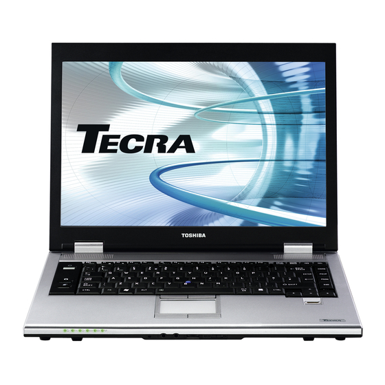
1 Hardware Overview 1.1 Features The front of the computer is shown in figure 1-1. Figure 1-1 Front of the computer [CONFIDENTIAL] TECRA A9(S5/P5/S200) Maintenance Manual (960-633) -
Page 21: Figure 1-2 System Unit Configuration
1.1 Features 1 Hardware Overview The system unit configuration is shown in figure 1-2. Figure 1-2 System unit configuration TECRA A9(S5/P5/S200) Maintenance Manual (960-633)[CONFIDENTIAL]... -
Page 22: Figure 1-3 System Unit Block Diagram
1 Hardware Overview 1.2 System Unit Block Diagram System Unit Block Diagram Figure 1-3 is a block diagram of the system unit. Figure 1-3 System unit block diagram [CONFIDENTIAL] TECRA A9(S5/P5/S200) Maintenance Manual (960-633) - Page 23 1.2 System Unit Block Diagram 1 Hardware Overview The system unit is composed of the following major components: Processor ® • Intel Core 2 Duo Processor • Core speed: • 2.40GHz (T7700) /2.20GHz (T7500) / 2.00GHz (T7300) In the case of Processor which built in 4MB L2 cache memory •...
- Page 24 1 Hardware Overview 1.2 System Unit Block Diagram Intel 965GM/GML (Crestline-GM (North Bridge)) • Features: – Meorom Processor System Bus Supports – PCI Express Based Graphics Interface – System Memory supports :DDR2-533/DDR2-667, 4GB max. – DMI(Direct Media Interface) – Power management control (ACPI2.0 conformity) Intel ICH8M (South Bridge) •...
- Page 25 1.2 System Unit Block Diagram 1 Hardware Overview Cardbus controller (TI PCI8412ZHK) − PCI Interface(PCI Rev.2.2) − SD IO Controller(Ver.1.1) − CardBus / Ultra media Controller (Yenta Ver.2.2:1 socket) − SD/MMC(SDHC Ver. 1.2 revised edition) , Memory Stick, Memory Stick pro, XD Card Controller −...
- Page 26 1 Hardware Overview 1.2 System Unit Block Diagram PSC (Power Supply Controller) • One TMP86FS49AUG chip is used. • This controller controls the power sources. Clock Generator • IDT 9LPR501PGLFT is used. • This device generates the system clock. Modem Controller •...
- Page 27 1.2 System Unit Block Diagram 1 Hardware Overview Wireless LAN • One PCI-Ex MiniCard • Intel Kedron a/b/g or a/b/g/n • Supports Wireless Communication SW • Supports W-LAN via PCMCIA (Euro : GSM/GPRS) Super I/O • SMSC LPC47N217-JV chip is used. •...
-
Page 28: Figure 1-4 3.5-Inch Fdd (Usb External)
1 Hardware Overview 1.3 3.5-inch Floppy Disk Drive (USB External) 3.5-inch Floppy Disk Drive (USB External) The 3.5-inch FDD is a thin, high-performance reliable drive that supports 720KB (formatted) 2DD and 1.44MB (formatted) 2HD disks. The FDD is shown in figure 1-4. The specifications for the FDD are listed in Table 1-1. Figure 1-4 3.5-inch FDD (USB External) Table 1-1 3.5-inch FDD specifications TEAC FD-05PUB-337... -
Page 29: Figure 1-5 2.5-Inch Hdd
1.4 2.5-inch Hard Disk Drive 1 Hardware Overview 2.5-inch Hard Disk Drive The removable HDD is a random access non-volatile storage device. It has a non-removable 2.5-inch magnetic disk and mini-Winchester type magnetic heads. The computer supports a 80GB, 120GB or 160GB. The HDD is shown in figure 1-5. -
Page 30: Optical Drive (Odd)
1 Hardware Overview 1.5 Optical Drive (ODD) Optical Drive (ODD) 1.5.1 CD-ROM Drive The CD-ROM drive accommodates either 12 cm (4.72-inch) or 8 cm (3.15-inch) CD-ROM. The specifications of the CD-ROM are described in Table 1-2. Table 1-2 CD-ROM drive specifications Specifications Item TEAC G8CC00039520... - Page 31 1.5 Optical Drive (ODD) 1 Hardware Overview 1.5.2 DVD-ROM & CD-R/RW Drive The DVD-ROM & CD-R/RW drive accommodates either 12 cm (4.72-inch) or 8 cm (3.15- inch) CD-ROM, DVD-ROM and CD-R/RW. The specifications of the DVD-ROM & CD-R/RW drive are described in Table 1-4. Table 1-4 DVD-ROM &...
-
Page 32: Dvd Super Multi Drive Specifications
1 Hardware Overview 1.5 Optical Drive (ODD) 1.5.3 DVD-Super Multi Drive The DVD Super Multi drive accommodates either 12 cm (4.72-inch) or 8 cm (3.15-inch) CD-ROM, DVD-ROM, CD-R, CD-RW, DVD-R, DVD+R, DVD-RW, DVD+RW, DVD- RAM, DVD-R DL and DVD+R DL. The specifications are listed in Table 1-5. -
Page 33: Keyboard
1.6 Keyboard 1 Hardware Overview Keyboard The keyboard is mounted 85(US)/87(UK) keys that consist of character key and control key, and in conformity with JIS. The keyboard is connected to membrane connector on the system board and controlled by the keyboard controller. Figure 1-6 is a view of the keyboard. -
Page 34: Tft Color Display
1 Hardware Overview 1.7 TFT Color Display TFT Color Display The TFT color display consists of 15.4-inch WXGA/WXGA+ LCD module and FL inverter board. 1.7.1 LCD Module The LCD module used for the TFT color display uses a backlight as the light source and can display a maximum of 16M colors with 1,280 x 800 or 1,680x1050 resolution. -
Page 35: Fl Inverter Board Specifications
1.7 TFT Color Display 1 Hardware Overview 1.7.2 FL Inverter Board The FL inverter board supplies a high frequency current to illuminate the LCD module. Table 1-5 lists the FL inverter board specifications. Table 1-5 FL inverter board specifications Item Specifications G71C0006A110 Input... -
Page 36: Power Supply
1 Hardware Overview 1.8 Power Supply Power Supply The power supply supplies many different voltages to the system board and performs the following functions: 1. Judges that the DC power supply (AC adapter) is connected to the computer. 2. Detects DC output and circuit malfunctions. 3. -
Page 37: Table 1-6 Power Supply Output Rating
1.8 Power Supply 1 Hardware Overview Table 1-6 Power supply output rating (1/4) Voltage (V) Name CK-EYV Clock Gen M-E3V 1.05 1R05-P1V 1R05-P1V 0.55-1.325 1.05 1R05M-E1V 1.05 1R05-P1V 1.25 1R25M-E1V 1.25 1R25-P1V (G)MCH 1R5-P1V 1R8-B1V 1.05 IGD-PGV 0R9-B0V Memory 1R8-B1V 1.05 1R05-P1V 1.25... - Page 38 1 Hardware Overview 1.8 Power Supply Table 1-6 Power supply output rating (2/4) Voltage (V) Name SB-P3V SB-P5V Card Cont. MCVCCA-PYV PC Card MCVPPA-PYV PC Card PS SD Card FM-P3V SD Card CRD1R5-P1V Express Card CRD-E3V CRD-P3V 1R5-P1V Express Card 1R5-P1V W-LAN 1-24...
- Page 39 1.8 Power Supply 1 Hardware Overview Table 1-6 Power supply output rating (3/4) Voltage (V) Name SIM Card UIMPWR-E3V 1R5-P1V Robson LAN-E3V EC/KBC Touch Pad SP-P5V Accelerometer FS-E3V Finger Sens. FS-E5V Finger Sens PS. Super I/O RS232C Driver 1.05 LN1R0- E1V LN1R8- E1V LNP -E3V LAN PS...
- Page 40 1 Hardware Overview 1.8 Power Supply Table 1-6 Power supply output rating (4/4) Voltage (V) Name 1R2-P1V 1R8-P1V 1.0-1.1 VRAM 1R8-P1V FL-P5V PNL-P3V LCD PS DVI Transmitter 2R5-P2V A4R7-P4V SND-P5V A4R7-P4V CODEC Headphone AMP 1-26 [CONFIDENTIAL] TECRA A9(S5/P5/S200) Maintenance Manual (960-633)
-
Page 41: Table 1-7 Battery Specifications
1.9 Batteries 1 Hardware Overview Batteries The computer has three types of batteries as follows: Main battery pack RTC battery The battery specifications are listed in Table 1-7. Table 1-7 Battery specifications Battery name Material Output Capacity voltage battery G71C00083110/210 Lithium-Ion 10.8 V 4,000 mAh... -
Page 42: Table 1-8 Time Required For Charges
1 Hardware Overview 1.9 Batteries 1.9.2 Battery Charging Control Battery charging is controlled by a power supply microprocessor. The microprocessor controls whether the charge is on or off and detects a full charge when the AC adaptor and battery are attached to the computer. The system charges the battery. Battery Charge When the AC adaptor is attached, there are two types of charge: When the system is powered off and when the system is powered on. -
Page 43: Table 1-9 Rtc Battery Charging/Data Preservation Time
1.9 Batteries 1 Hardware Overview 1.9.3 RTC battery The RTC battery provides power to keep the current date, time and other setup information in memory while the computer is turned off. Table 1-9 lists the charging time and data preservation period of the RTC battery. Table 1-9 RTC battery charging/data preservation time Status Time... -
Page 44: Table 1-10 Ac Adapter Specifications
1 Hardware Overview 1.10 AC Adapter 1.10 AC Adapter The AC adapter is also used to charge the battery. Table 1-10 lists the AC adapter specifications. Table 1-10 AC adapter specifications Parameter Specification G71C0006Q210 (2-pin) G71C0006R210 (3-pin) Power 75W (Peak 90W) Input voltage 100V/240V Input frequency... - Page 45 1.10 AC Adapter 1 Hardware Overview TECRA A9(S5/P5/S200) Maintenance Manual (960-633)[CONFIDENTIAL] 1-31...
-
Page 46: Troubleshooting Procedures
Chapter 2 Troubleshooting Procedures [CONFIDENTIAL]... - Page 47 2 Troubleshooting Procedures 2-ii [CONFIDENTIAL] TECRA A9(S5/P5/S200) Maintenance Manual (960-633)
- Page 48 2 Troubleshooting Procedures Chapter 2 Contents Troubleshooting......................2-1 Troubleshooting Flowchart ..................2-2 Power Supply Troubleshooting ..................2-6 Procedure 1 Icons in the LCD Check...............2-6 Procedure 2 Error Code Check ................2-7 Procedure 3 Connection Check ..............2-13 Procedure 4 Charge Check................2-14 Procedure 5 Replacement Check..............2-15 System Board Troubleshooting ................2-16 Procedure 1 Message Check ................2-17...
- Page 49 2 Troubleshooting Procedures Display Troubleshooting ..................2-42 Procedure 1 External Monitor Check.............2-42 Procedure 2 Diagnostic Test Program Execution Check .......2-42 Procedure 3 Connector Check and Cable Check ...........2-42 Procedure 4 Replacement Check..............2-43 Optical Drive Troubleshooting.................2-44 Procedure 1 Diagnostic Test Program Execution Check .......2-44 Procedure 2 Connector Check and Replacement Check........2-45 2.10...
- Page 50 2 Troubleshooting Procedures 2.16 Fingerprint sensor Troubleshooting .................2-59 Procedure 1 Setting Windows Log-ON password .........2-60 Procedure 2 Registration of fingerprint............2-60 Procedure 3 Authentication of fingerprint .............2-67 Procedure 4 Connector Check and Replacement Check........2-68 TECRA A9(S5/P5/S200) Maintenance Manual (960-633)[CONFIDENTIAL]...
- Page 51 2 Troubleshooting Procedures Figures Figure 2-1 Troubleshooting flowchart ..................2-3 Figure 2-2 Printer port LED board ..................2-19 Figure 2-3 Function of Printer port LED................2-19 Tables Table 2-1 Battery icon......................2-6 Table 2-2 DC IN icon......................2-6 Table 2-3 Error code ......................2-7 Table 2-4 Result code ......................2-14 Table 2-5 Printer port LED boot mode status ..............2-21 Table 2-6 FDD error code and status .................2-34 Table 2-7 HDD error code and status ................2-39...
-
Page 52: Troubleshooting
2.1 Troubleshooting 2 Troubleshooting Procedures Troubleshooting Chapter 2 describes how to determine if a Field Replaceable Unit (FRU) in the computer is causing the computer to malfunction. The FRUs covered are: 1. Power Supply 6. Display 11. Wireless LAN 2. System Board 7. -
Page 53: Troubleshooting Flowchart
Ask the user if a password is registered and, if it is, ask him or her to enter the password. Make sure that Toshiba Windows is installed on the hard disk. Non-Toshiba operating systems can cause the computer malfunction. Make sure all optional equipment is removed from the computer. - Page 54 2.2 Troubleshooting Flowchart 2 Troubleshooting Procedures Figure 2-1 Troubleshooting flowchart (1/2) TECRA A9(S5/P5/S200) Maintenance Manual (960-633)[CONFIDENTIAL]...
- Page 55 2 Troubleshooting Procedures 2.2 Troubleshooting Flowchart Figure 2-1 Troubleshooting flowchart (2/2) [CONFIDENTIAL] TECRA A9(S5/P5/S200) Maintenance Manual (960-633)
- Page 56 2.2 Troubleshooting Flowchart 2 Troubleshooting Procedures If the diagnostics program cannot detect an error, the problem may be intermittent. The Running Test program should be executed several times to isolate the problem. Check the Log Utilities function to confirm which diagnostic test detected an error, then perform the appropriate troubleshooting procedures as follows: 1.
-
Page 57: Power Supply Troubleshooting
2 Troubleshooting Procedures 2.3 Power Supply Troubleshooting Power Supply Troubleshooting The power supply controls many functions and components. To determine if the power supply is functioning properly, start with Procedure 1 and continue with the other Procedures as instructed. The procedures described in this section are: Procedure 1: Icons in the LCD Check Procedure 2: Error Code Check Procedure 3: Connection Check... - Page 58 2.3 Power Supply Troubleshooting 2 Troubleshooting Procedures Procedure 2 Error Code Check If the power supply microprocessor detects a malfunction, it indicates the error code as shown below. The error code begins with the least significant digit. Table 2-3 Error code Error code Where Error occurs AC Adaptor...
- Page 59 2 Troubleshooting Procedures 2.3 Power Supply Troubleshooting Check 1 Compare the patterns in the hexadecimal error code to the tables below. AC Adaptor Error code Meaning AC Adaptor output voltage is over 16.5V. Express Port Replicator voltage is over 16.5V. Current from the DC power supply is over 7.00A.
- Page 60 2.3 Power Supply Troubleshooting 2 Troubleshooting Procedures 1R5-C1V output (P62) Error code Meaning 1R5-C1V voltage is over 2.15V when the computer is powered on/off. 1R5-C1V voltage is 1.275V or less when the computer is powered on. 1R5-C1V voltage is 1.275V or less when the computer is booting up 1R5-C1V voltage is 1.275V or less when the computer is suspended.
- Page 61 2 Troubleshooting Procedures 2.3 Power Supply Troubleshooting 1R9-B1V output (P66:MUX- CH0) Error code Meaning 1R9-B1V voltage is over 2.40V when the computer is powered on/off. 1R9-B1V voltage is 1.53V or less when the computer is powered on. 1R9-B1V voltage is 1.53V or less when the computer is booting up 1R9-B1V voltage is 1.53 or more when the computer is powered off.
- Page 62 2.3 Power Supply Troubleshooting 2 Troubleshooting Procedures 1R9-B1V output (P66:MUX- CH1) Error code Meaning 1R9-B1V voltage is over 2.40V when the computer is powered on/off. 1R9-B1V voltage is 1.53V or less when the computer is powered on. 1R9-B1V voltage is 1.53V or less when the computer is booting up 1R9-B1V voltage is 1.53 or more when the computer is powered off.
- Page 63 2 Troubleshooting Procedures 2.3 Power Supply Troubleshooting Check 2 In the case of error code 10h or 12h: Make sure the AC adaptor cord and AC power cord are firmly plugged into the DC IN 15 V socket and wall outlet. If the cables are connected correctly, go to the following step: Connect a new AC adaptor and/or AC power cord, if necessary.
-
Page 64: Procedure 3 Connection Check
2.3 Power Supply Troubleshooting 2 Troubleshooting Procedures Procedure 3 Connection Check The power supply wiring diagram is shown below: Any of the connectors may be disconnected. Perform Check 1. Check 1 Disconnect the AC power cord from the wall outlet. Check the power cable for breaks. - Page 65 2 Troubleshooting Procedures 2.3 Power Supply Troubleshooting Procedure 4 Charge Check The power supply may not charge the battery pack. Perform the following procedures: 1. Reinstall the battery pack. 2. Attach the AC adaptor and turn on the power. If you cannot turn on the power, go to Procedure 5.
-
Page 66: Procedure 5 Replacement Check
2.3 Power Supply Troubleshooting 2 Troubleshooting Procedures Procedure 5 Replacement Check The system board processor module may be disconnected or damaged. Disassemble the computer following the steps described in Chapter 4, Replacement Procedures. Check the connection between the AC adaptor and system board and connection. After checking the connections, perform the following Check 1: Check 1 Replace the AC adaptor with a new one. -
Page 67: System Board Troubleshooting
2 Troubleshooting Procedures 2.4 System Board Troubleshooting System Board Troubleshooting This section describes how to determine if the system board and CPU are defective or not functioning properly. Start with Procedure 1 and continue with the other procedures as instructed. The procedures described in this section are: Procedure 1: Message Check Procedure 2: Printer Port LED Check on Boot Mode... - Page 68 2.4 System Board Troubleshooting 2 Troubleshooting Procedures Procedure 1 Message Check When the power is turned on, the system performs the Initial Reliability Test (IRT) installed in the BIOS ROM. The IRT tests each IC on the system board and initializes it. If an error message is shown on the display, perform Check 1.
- Page 69 2 Troubleshooting Procedures 2.4 System Board Troubleshooting Check 2 The IRT checks the system board. When the IRT detects an error, the system stops or an error message appears. If one of the following error messages (1) through (17), (22) or (23) appears, go to Procedure 4.
- Page 70 2.4 System Board Troubleshooting 2 Troubleshooting Procedures Procedure 2 Serial Port Check (Boot Mode) Check the D port status by a serial port test. The tool for serial port test is shown below. Figure 2-2 A set of tool for serial port test The test procedures are follows: 1.
- Page 71 2 Troubleshooting Procedures 2.4 System Board Troubleshooting Table 2-5 Serial port (Boot mode) error status (1/9) D port Test item Contents Status Boot Block Permission of A20 and clear of software reset bit Prohibition of APIC Initialization of MCH, ICH Initialization of Super I/O Initialization of debug port (For models supporting debug port)
- Page 72 2.4 System Board Troubleshooting 2 Troubleshooting Procedures Table 2-5 Serial port (Boot mode) error status (2/9) D port Test item Contents Status F0B9h Saving of key scan code Setting of TASK_1ms_TSC FAN control Sound initialization (for BEEP sound) System speaker permission Cancel of sound mute Setting of volume to max (model that can control volume)
- Page 73 2 Troubleshooting Procedures 2.4 System Board Troubleshooting Table 2-5 Serial port (Boot mode) error status (3/9) D port Test item Message Status F100h Renewal of a microcode (Only support model) Prohibition of cache Permission of L1/L2 cache in FlashROM area Initialization of H/W (before Initialization of MCH DRAM recognition)
- Page 74 2.4 System Board Troubleshooting 2 Troubleshooting Procedures Table 2-5 Serial port (Boot mode) error status (4/9) Test item Contents D port Status (F103h) Check of memory configuration change (Resume error LED=73H) RAM area checksum check in system BIOS (Resume error LED=79H) Expansion memory checksum check resume error (Resume error LED=76H) PnP RAM checksum check (Resume...
- Page 75 2 Troubleshooting Procedures 2.4 System Board Troubleshooting Table 2-5 Serial port (Boot mode) error status (5/9) D port Status Test item Contents (F106h) Check of parameter block A Permission of SMI except auto-off function Control of excess of rated input power Battery discharging current control (1CmA).
- Page 76 2.4 System Board Troubleshooting 2 Troubleshooting Procedures Table 2-5 Serial port (Boot mode) error status (6/9) D port Status Test item Contents F108h PCI bus initialization (connection of DS Bus) Initialization of LAN information WakeUp factor check Task generation for waiting INIT_PCI F109h completion CMOS data initialization (2)
- Page 77 2 Troubleshooting Procedures 2.4 System Board Troubleshooting Table 2-5 Serial port (Boot mode) error status (7/9) D port Status Test item Contents F10Fh INIT_SYSTEM (Initialization of system) Storing of CMOS error information to IRT_ERR_STS_BUF Timer initialization start EC initialization & Reading of battery information Update of system BIOS (Update EDID information for LCD) F110h...
- Page 78 2.4 System Board Troubleshooting 2 Troubleshooting Procedures Table 2-5 Serial port (Boot mode) error status (8/9) D port Status Test item Contents (F11Dh) I/O LOCK Processing (For models supporting I/O LOCK) Opening of BM (Only model which is supporting the finger point leader) F11Eh EX_IO_ROM_CHECK...
- Page 79 2 Troubleshooting Procedures 2.4 System Board Troubleshooting Table 2-5 Serial port (Boot mode) error status (9/9) D port Status Test item Contents (F11Fh) HW initialization before Boot, Waiting for initialization completion Notifies the DVI connection status to VGA BIOS (For models supporting DVI) Setting of battery save mode Setting of date Waiting for Bluetooth initialization completion...
- Page 80 2.4 System Board Troubleshooting 2 Troubleshooting Procedures Procedure 3 Diagnostic Test Program Execution Check Execute the following tests from the Diagnostic Test Menu. Refer to Chapter 3, Tests and Diagnostics, for more information on how to perform these tests. 1. System test 2.
-
Page 81: Procedure 4 Replacement Check
2 Troubleshooting Procedures 2.4 System Board Troubleshooting Procedure 4 Replacement Check The system board connectors may be disconnected. Disassemble the computer following the steps described in Chapter 4, Replacement Procedures and perform Check 1. Check 1 Visually check for the following: a) Cracked or broken connector housing b) Damaged connector pins If their connectors are in good condition, but there is still a problem, go to Check... -
Page 82: Usb Fdd Troubleshooting
2.5 USB FDD Troubleshooting 2 Troubleshooting Procedures USB FDD Troubleshooting This section describes how to determine if the USB FDD is functioning properly. Perform the steps below starting with Procedure 1 and continuing with the other procedures as required. Procedure 1: USB FDD Head Cleaning Check Procedure 2: Diagnostic Test Program Execution Check Procedure 3: Connector Check and Replacement Check Procedure 1... - Page 83 2 Troubleshooting Procedures 2.5 USB FDD Troubleshooting Procedure 2 Diagnostic Test Program Execution Check Insert the Diagnostics Disk in the USB FDD, turn on the computer and run the test. Refer to Chapter 3, Tests and Diagnostics, for more information about the diagnostics test procedures. Floppy disk drive test error codes and their status names are listed in Table 2-6.
- Page 84 2.5 USB FDD Troubleshooting 2 Troubleshooting Procedures Procedure 3 Connector Check and Replacement Check The USB FDD is connected to the System Board. Check 1 When using the USB port, make sure the USB FDD cable is firmly connected to CN4612 , CN4611 or CN4610 on the System board.
-
Page 85: Hdd Troubleshooting
2 Troubleshooting Procedures 2.6 HDD Troubleshooting HDD Troubleshooting This section describes how to determine if the HDD is functioning properly. Perform the steps below starting with Procedure 1 and continuing with the other procedures as required. Procedure 1: Message Check Procedure 2: Partition Check Procedure 3: Format Check Procedure 4: Diagnostic Test Program Execution Check... -
Page 86: Procedure 2 Partition Check
Procedure 2 Partition Check Insert the Toshiba MS-DOS system disk and restart the computer with U key holding down. Perform the following checks: Type C: and press Enter. If you cannot change to drive C, go to Check 2. If you Check 1 can change to drive C, go to Check 3. - Page 87 Check 1 following message appears on the display, the HDD is formatted. Format complete If an error message appears on the display, refer to the Toshiba MS-DOS Manual for more information and perform Check 2. Check 2 Using the Diagnostics Disk, format the HDD with a low level format option.
-
Page 88: Procedure 4 Diagnostic Test Program Execution Check
2.6 HDD Troubleshooting 2 Troubleshooting Procedures Procedure 4 Diagnostic Test Program Execution Check The HDD test program is stored in the Diagnostics Disk. Perform all of the HDD tests in the Hard Disk Drive Test. Refer to Chapter 3, Tests and Diagnostics, for more information about the HDD test program. - Page 89 2 Troubleshooting Procedures 2.6 HDD Troubleshooting Procedure 5 Connector Check and Replacement Check The HDD may be disconnected, or the HDD or the system board may be damaged. Disassemble the computer following the steps described in Chapter 4, Replacement Procedures and perform the following checks: Check 1 Make sure the HDD is firmly connected to CN19000 on the system board.
-
Page 90: Keyboard And Dual Point Troubleshooting
2.7 Keyboard and Dual point Troubleshooting 2 Troubleshooting Procedure Keyboard and Dual point Troubleshooting To determine if the computer’s keyboard or touch pad is functioning properly, perform the following procedures. Start with Procedure 1 and continue with the other procedures as instructed. - Page 91 2 Troubleshooting Procedures 2.7 Keyboard and Dual point Troubleshooting Procedure 2 Connector Check and Replacement Check The keyboard, Dual point or sensor/switch board may be disconnected or damaged. Disassemble the computer following the steps described in Chapter 4, Replacement Procedures, and perform the following checks: 1.
- Page 92 2.7 Keyboard and Dual point Troubleshooting 2 Troubleshooting Procedure Check 5 The system board may be damaged. Replace it with a new one following the instructions in Chapter 4, Replacement Procedures. TECRA A9(S5/P5/S200) Maintenance Manual (960-633)[CONFIDENTIAL] 2-41...
-
Page 93: Display Troubleshooting
2 Troubleshooting Procedures 2.8 Display Troubleshooting Display Troubleshooting This section describes how to determine if the computer’s display is functioning properly. Start with Procedure 1 and continue with the other procedures as instructed. Procedure 1: External Monitor Check Procedure 2: Diagnostic Test Program Execution Check Procedure 3: Connector Check and Cable Check Procedure 4: Replacement Check Procedure 1... - Page 94 2.8 Display Troubleshooting 2 Troubleshooting Procedures If the connection is loose, reconnect firmly and restart the computer. If there is still an error, go to Procedure 4. Procedure 4 Replacement Check The FL, FL inverter board, LCD module, and system board are connected to display circuits. Any of these components may be damaged.
-
Page 95: Optical Drive Troubleshooting
2 Troubleshooting Procedures 2.9 Optical Drive Troubleshooting Optical Drive Troubleshooting This section describes how to determine if the optical drive (Super Multi drive) in the Slim Select Bay is functioning properly. Perform the steps below starting with Procedure 1 and continue with the other procedures as required. - Page 96 2.9 Optical Drive Troubleshooting 2 Troubleshooting Procedures Procedure 2 Connector Check and Replacement Check The optical drive (Super Multi drive) is connected to the system board. The connectors may be disconnected from the system board or may be damaged. Disassemble the computer following the steps described in Chapter 4, Replacement Procedures and perform the following checks: Check 1...
-
Page 97: Modem Troubleshooting
2 Troubleshooting Procedures 2.10 Modem Troubleshooting 2.10 Modem Troubleshooting This section describes how to determine if the computer’s modem is functioning properly. Perform the steps below starting with Procedure 1 and continuing with the other procedures as required. Procedure 1: Diagnostic Test Program Execution Check Procedure 2: Connector Check and Replacement Check Procedure 1 Diagnostic Test Program Execution Check... - Page 98 2.10 Modem Troubleshooting 2 Troubleshooting Procedures Procedure 2 Connector Check and Replacement Check The Modem is installed as a MDC (Modem Daughter Card). If the modem malfunctions, there may be a bad connection between the MDC and the system board. Or the MDC, system board or their connectors might be damaged.
-
Page 99: Lan Troubleshooting
2 Troubleshooting Procedures 2.11 LAN Troubleshooting 2.11 LAN Troubleshooting This section describes how to determine if the computer’s LAN is functioning properly. Perform the steps below starting with Procedure 1 and continue with the other procedures as required. Procedure 1: Diagnostic Test Program Execution Check Procedure 2: Connector Check and Replacement Check Procedure 1 Diagnostic Test Program Execution Check... -
Page 100: Bluetooth Troubleshooting
2.12 Bluetooth Troubleshooting 2 Troubleshooting Procedures 2.12 Bluetooth Troubleshooting This section describes how to determine if the computer’s Bluetooth is functioning properly. Perform the steps below starting with Procedure 1 and continuing with the other procedures as required. Procedure 1: Diagnostic Test Program Execution Check Procedure 2: Connection Check Procedure 3: Replacement Check Procedure 1... -
Page 101: Procedure 2 Connection Check
2 Troubleshooting Procedures 2.12 Bluetooth Troubleshooting Procedure 2 Connection Check The Bluetooth function wiring diagram is shown below: Any of the connections may be disconnected. Disassemble the computer following the steps described in Chapter 4, Replacement Procedures, and perform the following checks: Check 1 Make sure the Bluetooth module is firmly connected to CN4400 on the sound board. -
Page 102: Procedure 3 Replacement Check
2.12 Bluetooth Troubleshooting 2 Troubleshooting Procedures Procedure 3 Replacement Check The Bluetooth antenna, Bluetooth module, sound board and system board are connected to the circuits. Any of these components may be damaged. Refer to Chapter 4, Replacement Procedures, for instructions on how to disassemble the computer and then perform the following checks: Check 1 The Bluetooth module may be defective or damaged. -
Page 103: Wireless Lan Troubleshooting
2 Troubleshooting Procedures 2.13 Wireless LAN Troubleshooting 2.13 Wireless LAN Troubleshooting This section describes how to determine if the computer’s Wireless LAN is functioning properly. Perform the steps below starting with Procedure 1 and continuing with the other procedures as required. Procedure 1: Transmitting-Receiving Check Procedure 2: Antenna Connection Check Procedure 3: Replacement Check... - Page 104 2.13 Wireless LAN Troubleshooting 2 Troubleshooting Procedures Procedure 2 Antenna Connection Check The wireless LAN wiring diagram is shown below: Any of the connections may be disconnected. Disassemble the computer following the steps described in Chapter 4, Replacement Procedures, and perform the following checks: Check 1 Make sure the wireless LAN board is firmly connected to CN2600 on the system board.
- Page 105 2 Troubleshooting Procedures 2.13 Wireless LAN Troubleshooting Procedure 3 Replacement Check The wireless LAN antenna, wireless LAN board and the system board are connected to the circuits. Any of these components may be damaged. Refer to Chapter 4, Replacement Procedures, for instructions on how to disassemble the computer and then perform the following checks: Check 1 The wireless LAN board may be defective or damaged.
-
Page 106: Sound Troubleshooting
2.14 Sound Troubleshooting 2 Troubleshooting Procedures 2.14 Sound Troubleshooting This section describes how to determine if the computer’s sound functions are functioning properly. Perform the steps below starting with Procedure 1 and continuing with the other procedures as required. Procedure 1: Diagnostic Test Program Execution Check Procedure 2: Connecor Check Procedure 3: Replacement Check Procedure 1... -
Page 107: Procedure 2 Connector Check
2 Troubleshooting Procedures 2.14 Sound Troubleshooting Procedure 2 Connector Check The sound function-wiring diagram is shown below: Any of the connections may be disconnected. Disassemble the computer following the steps described in Chapter 4, Replacement Procedures and perform the following checks: 1. - Page 108 2.14 Sound Troubleshooting 2 Troubleshooting Procedures Procedure 3 Replacement Check Check 1 If the speakers do not sound properly, the speaker may be defective or damaged. Replace it with a new one. If the speakers still do not work properly, go to Check Check 2 If the Built in microphone do not sound properly, the Built in microphone may be defective or damaged.
-
Page 109: Bridge Media Slot Troubleshooting
2 Troubleshooting Procedures 2.15 Bridge media Slot Troubleshooting 2.15 Bridge media Slot Troubleshooting This section describes how to determine if the computer's Bridge media functions are functioning properly. Perform the steps below starting with Procedure 1 and continuing with the other procedures as required. Procedure 1: Check on Windows OS Procedure 2: Connector Check and Replacement Check Procedure 1... -
Page 110: Fingerprint Sensor Troubleshooting
2.16 Fingerprint sensor Troubleshooting 2 Troubleshooting Procedures 2.16 Fingerprint sensor Troubleshooting CAUTION: To delete the account for confirming the fingerprint operation, it is necessary to log on by the account with the management authority. If the password has been set to log on, ask the Log-ON password to the user. To check if the Fingerprint sensor works correctly or not, follow the troubleshooting procedures below as instructed. - Page 111 2 Troubleshooting Procedures 2.16 Fingerprint sensor Troubleshooting Procedure 1 Setting Windows Log-ON password 1. Open [User Account] from [Control Panel]. 2. Click [User Account]. 3. Click the icon of the account (user’s name) that you want to set the password. 4.
- Page 112 2.16 Fingerprint sensor Troubleshooting 2 Troubleshooting Procedures [User's Passport] appears in “Enter your password”. Click [Next]. When the finger print has been enrolled, [User’s Password] appears. Slide your finger enrolled or type the password. Click [Next]. 5. Type the Windows logon password in “Enter your password” and click [Next]. [User’s Password] appears.
- Page 113 2 Troubleshooting Procedures 2.16 Fingerprint sensor Troubleshooting 6. Confirm that the box of [Run interactive tutorial] is checked (when proceeding wit seeing Tutorial) and click [Next]. 7. Watch the Video carefully, click [Next]. 2-62 [CONFIDENTIAL] TECRA A9(S5/P5/S200) Maintenance Manual (960-633)
- Page 114 2.16 Fingerprint sensor Troubleshooting 2 Troubleshooting Procedures 8. Put lightly your finger on the fingerprint sensor at the right side of the touchpad panel and slide your finger sideways Slide your finger four times. Four boxes are filled with fingerprints. At this time, when you click the [Replay video], you can watch the video that you have watched in Procedure 6.
- Page 115 2 Troubleshooting Procedures 2.16 Fingerprint sensor Troubleshooting When you have failed in any time of four times reading and want to practice again, click [Try again]. When you have fully succeeded in four times of reading, the message of “Fully succeeded” appears. 9.
- Page 116 2.16 Fingerprint sensor Troubleshooting 2 Troubleshooting Procedures Put lightly the first joint of your finger you want to enroll on the fingerprint sensor and slide your finger sideways. Enroll your finger three times. Every time your finger has been successfully enrolled, one box is checked. When your finger has been successfully enrolled three times, the message of “Succeeded”...
- Page 117 2 Troubleshooting Procedures 2.16 Fingerprint sensor Troubleshooting 13. Type a backup password two times in the following display. (This password is different from the password of Windows logon.) 14. Click [Next]. The [Finish] display appears. 15. Click [Finish], “Welcome” display appears. 2-66 [CONFIDENTIAL] TECRA A9(S5/P5/S200) Maintenance Manual (960-633)
- Page 118 2.16 Fingerprint sensor Troubleshooting 2 Troubleshooting Procedures Procedure 3 Authentication of fingerprint 1. Turn on the computer to start up Windows. 2. In the Windows logon window, put lightly the first joint of your finger registered and slide your finger sideways. When authenticated, [Success] is displayed in the fingerprint authentication display.
- Page 119 2 Troubleshooting Procedures 2.16 Fingerprint sensor Troubleshooting Procedure 4 Connector Check and Replacement Check The Fingerprint sensor cable is connected to the connector CN9650 on the Fingerprint sensor board and connector CN9550 on the system board. Check 1 Check the Fingerprint sensor cable is firmly connected to the connector CN9650 on the Fingerprint sensor board and connector CN9550 on the system board.
-
Page 120: Tests And Diagnostics
Chapter 3 Tests and Diagnostics [CONFIDENTIAL]... - Page 121 3 Tests and Diagnostics 3-ii [CONFIDENTIAL] TECRA A9(S5/P5/S200) Maintenance Manual (960-633)
- Page 122 3 Tests and Diagnostics Chapter 3 Contents The Diagnostic Test ....................3-1 3.1.1 Diagnostics menu ................. 3-1 3.1.2 H/W (Hardware) initial information setting tool........3-3 3.1.3 Heatrun test program................3-3 Executing the Diagnostic Test ................... 3-4 3.2.1 Diagnostics menu (T&D) ..............3-5 3.2.2 H/W initial information setting tool .............
- Page 123 3 Tests and Diagnostics 3.21 Head Cleaning......................3-48 3.21.1 Function Description ................3-48 3.21.2 Operations ..................3-48 3.22 Log Utilities ......................3-49 3.22.1 Function Description ................3-49 3.22.2 Operations ..................3-50 3.23 Running Test......................3-51 3.23.1 Function Description ................3-51 3.23.2 Operations ..................
- Page 124 3 Tests and Diagnostics 3.30 BIOS SETUP ......................3-86 3. 30.1 Function Description ................3-86 3. 30.2 Accessing the BIOS SETUP Program ..........3-88 Tables Table 3-1 Subtest names ....................3-12 Table 3-2 Error codes and error status names ..............3-35 Table 3-3 Hard disk controller status register contents............
- Page 125 3 Tests and Diagnostics 3-vi [CONFIDENTIAL] TECRA A9(S5/P5/S200) Maintenance Manual (960-633)
-
Page 126: The Diagnostic Test
3.1 The Diagnostic Test 3 Tests and Diagnostics The Diagnostic Test This chapter explains how to use the Diagnostic Test programs to test the functions of the computer’s hardware modules. The Diagnostics Programs are stored on some Diagnostic Disks. There are Service Program Modules (DIAGNOSTIC MENU) and the Test Program Modules (DIAGNOSTIC TEST MENU) on the Diagnostic Disk. - Page 127 A USB test module (USB test ) A USB cable (USB test) An external CRT monitor (Expansion test) A CD test media TOSHIBA CD-ROM TEST DISK or ABEX TEST CD-ROM (Sound test) A DVD test media (DVD-ROM TEST DISK TSD-1) (Sound test)
-
Page 128: H/W (Hardware) Initial Information Setting Tool
3.1 The Diagnostic Test 3 Tests and Diagnostics 3.1.2 H/W (Hardware) initial information setting tool The H/W initial information setting tool consists of the following programs. Initial configuration DMI information save DMI information recovery System configuration display E2PROM test (MAC/GUID/DMI) You will need the following equipment to perform some of the programs. -
Page 129: Executing The Diagnostic Test
3 Tests and Diagnostics 3.2 Executing the Diagnostic Test Executing the Diagnostic Test To start the DIAGNOSTIC PROGRAM, follow these steps: 1. Insert the Diagnostics disk in the USB floppy disk drive. 2. Turn on the computer while pressing U key. The following menu appears. Repair test program 1 Repair Main 2 Repair Initial config set... -
Page 130: Diagnostics Menu (T&D)
Enter in the startup menu, press Repair Main Enter. The following menu appears. TOSHIBA personal computer XXXXXX DIAGNOSTICS version X.XX (c) copyright TOSHIBA Corp. 20XX DIAGNOSTICS MENU : 1 - DIAGNOSTIC TEST 2 – ONLY ONE TEST 4 - HEAD CLEANING... - Page 131 Set the highlight bar to 1, and press Enter. The following DIAGNOSTIC TEST MENU will appear: TOSHIBA personal computer XXXXXX DIAGNOSTICS version X.XX (c) copyright TOSHIBA Corp. 20XX DIAGNOSTIC TEST MENU : 1 - SYSTEM TEST 2 - MEMORY TEST...
- Page 132 3.2 Executing the Diagnostic Test 3 Tests and Diagnostics Select the option you want to execute and press Enter. When you select 1- SYSTEM TEST, the following message will appear: SYSTEM TEST NAME XXXXXX xxxxxxx DIAGNOSTIC TEST VX.XX [Ctrl]+[Break] : test end [Ctrl]+[C] : key stop SUB-TEST...
-
Page 133: Repair Initial Config Set
3 Tests and Diagnostics 3.2 Executing the Diagnostic Test Selecting YES of ERROR STOP stops the test program when an error is found and displays the operation guide on the right side of the display screen as shown below: ERROR STATUS NAME [[ HALT OPERATION ]] 1: Test end 2: Continue... -
Page 134: Setting Of The Hardware Configuration
3.3 Setting of the hardware configuration 3 Tests and Diagnostics Setting of the hardware configuration To execute this program, 2, Repair Initial config set and press Enter in the startup menu, press Enter and follow the directions on the screen. The H/W initial information setting tool consists of four subtests. - Page 135 3 Tests and Diagnostics 3.3 Setting of the hardware configuration 7. “Create DMIINFO TXT (Y/N) ?” is displayed. Press Y, then the DMI information (text data) is written to the Floppy disk, etc. Setting of the HWSC • Setting of the UUID •...
-
Page 136: Heatrun Test
3.4 Heatrun Test 3 Tests and Diagnostics Heatrun Test To execute this program, press 3, Repair Heatrun and press Enter in the startup menu, press Enter. After selecting this test, the same subtests as 3.23 Running Test are executed successively. For more details on the procedure and test content, refer to Running Test. -
Page 137: Subtest Names
3 Tests and Diagnostics 3.5 Subtest Names Subtest Names Table 3-1 lists the subtest names for each test program in the DIAGNOSTIC TEST MENU. Table 3-1 Subtest names (1/2) Test Name Subtest No. Subtest Name SYSTEM ROM checksum Fan ON/OFF Geyserville Quick charge DMI read... - Page 138 3.5 Subtest Names 3 Tests and Diagnostics Table 3-1 Subtest names (2/2) Test Name Subtest No. Subtest Name PRINTER Ripple pattern Function [It is not Wraparound supported ] FIR/SIR Point to point (send) ASYNC FIR/SIR Point to point (receive) Wraparound (board) HARD DISK Sequential read Address uniqueness...
-
Page 139: System Test
3 Tests and Diagnostics 3.6 System Test System Test To execute the System Test, select 1 from the DIAGNOSTIC TEST MENU, press Enter and follow the directions on the screen. Move the highlight bar to the subtest you want to execute and press Enter. - Page 140 3.6 System Test 3 Tests and Diagnostics Subtest 04 Quick charge This subtest checks the status for the quick charge. Subtest 05 DMI read This subtest displays the information in the Flash-ROM in the following format. *** DMI Data Display Ver X.XX *** Model Name : XXXXXXXXXXX Version Number...
-
Page 141: Memory Test
3 Tests and Diagnostics 3.7 Memory Test Memory Test To execute the Memory Test, select 2 from the DIAGNOSTIC TEST MENU, press Enter and follow the directions on the screen. Move the highlight bar to the subtest you want to execute and press Enter. -
Page 142: Keyboard Test
3.8 Keyboard Test 3 Tests and Diagnostics Keyboard Test To execute the Keyboard Test, select 3 from the DIAGNOSTIC TEST MENU, press Enter and follow the directions on the screen. Move the highlight bar to the subtest you want to execute and press Enter. -
Page 143: Display Test
3 Tests and Diagnostics 3.9 Display Test Display Test To execute the Display Test, select 4 from the DIAGNOSTIC TEST MENU, press Enter and follow the directions on the screen. Move the highlight bar to the subtest you want to execute and press Enter. - Page 144 3.9 Display Test 3 Tests and Diagnostics Subtest 04 Gradation & Mode test for VGA This subtest displays gradations for following modes. To change the mode, press Enter. [Mode 12] [Mode 13] [Mode 3] [Mode 111 640*480 64K] [Mode 112 640*480 16M] [Mode 114 800*600 64K]...
- Page 145 3 Tests and Diagnostics 3.9 Display Test Subtest 06 “H” pattern display This subtest displays a full screen of “H” patterns. HHHHHHHHHHHHHHHHHHHHHHHHHHHHHHHHHHHHHHHHHHHHHHHHHH HHHHHHHHHHHHHHHHHHHHHHHHHHHHHHHHHHHHHHHHHHHHHHHHHH HHHHHHHHHHHHHHHHHHHHHHHHHHHHHHHHHHHHHHHHHHHHHHHHHH HHHHHHHHHHHHHHHHHHHHHHHHHHHHHHHHHHHHHHHHHHHHHHHHHH HHHHHHHHHHHHHHHHHHHHHHHHHHHHHHHHHHHHHHHHHHHHHHHHHH HHHHHHHHHHHHHHHHHHHHHHHHHHHHHHHHHHHHHHHHHHHHHHHHHH HHHHHHHHHHHHHHHHHHHHHHHHHHHHHHHHHHHHHHHHHHHHHHHHHH HHHHHHHHHHHHHHHHHHHHHHHHHHHHHHHHHHHHHHHHHHHHHHHHHH HHHHHHHHHHHHHHHHHHHHHHHHHHHHHHHHHHHHHHHHHHHHHHHHHH HHHHHHHHHHHHHHHHHHHHHHHHHHHHHHHHHHHHHHHHHHHHHHHHHH HHHHHHHHHHHHHHHHHHHHHHHHHHHHHHHHHHHHHHHHHHHHHHHHHH HHHHHHHHHHHHHHHHHHHHHHHHHHHHHHHHHHHHHHHHHHHHHHHHHH HHHHHHHHHHHHHHHHHHHHHHHHHHHHHHHHHHHHHHHHHHHHHHHHHH HHHHHHHHHHHHHHHHHHHHHHHHHHHHHHHHHHHHHHHHHHHHHHHHHH HHHHHHHHHHHHHHHHHHHHHHHHHHHHHHHHHHHHHHHHHHHHHHHHHH To exit this subtest and return to the DISPLAY TEST menu, press Enter. NOTE: The last row may not be completely filled.
-
Page 146: Floppy Disk Test
3.10 Floppy Disk Test 3 Tests and Diagnostics 3.10 Floppy Disk Test CAUTION: Before running the floppy disk test, prepare a formatted work disk. Remove the Diagnostics Disk and insert the work disk into the FDD because the contents of the floppy disk will be erased. To execute the Floppy Disk Test, select 5 from the DIAGNOSTIC TEST MENU, press Enter and follow the directions displayed on the screen. - Page 147 3 Tests and Diagnostics 3.10 Floppy Disk Test Select the number of the subtest you want to execute and press Enter. The following message will appear during the floppy disk test. xxx DIAGNOSTIC TEST VX.XX FLOPPY DISK IN PROGRESS XXXXXXX [Ctrl]+[Break] : test end [Ctrl]+[C]...
-
Page 148: Printer Test
3.11 Printer Test 3 Tests and Diagnostics 3.11 Printer Test NOTE: Printer Test is not supported for this model. To execute the Printer Test, select 6 from the DIAGNOSTIC TEST MENU, press Enter and follow the directions on the screen. NOTE: An IBM compatible printer must be connected to the system to execute this test. - Page 149 3 Tests and Diagnostics 3.11 Printer Test Subtest 02 Function This subtest is for IBM compatible printers, and tests the following functions: Normal print Double-width print Compressed print Emphasized print Double-strike print All characters print This subtest prints the various print types shown below: Subtest 03 Wraparound NOTE: To execute this subtest, a printer wraparound connector must be connected to the...
-
Page 150: Async Test
3.12 Async Test 3 Tests and Diagnostics 3.12 Async Test To execute the Async Test, select 7 from the DIAGNOSTIC TEST MENU, press Enter and follow the directions displayed on the screen. Move the highlight bar to the subtest you want to execute and press Enter. -
Page 151: Hard Disk Test
3 Tests and Diagnostics 3.13 Hard Disk Test 3.13 Hard Disk Test To execute the Hard Disk Test, select 8 from the DIAGNOSTIC TEST MENU, press Enter, and follow the directions on the screen. CAUTION: The contents of the hard disk will be erased when subtest 02, 03, 04, 06, 08 or 09 is executed. - Page 152 3.13 Hard Disk Test 3 Tests and Diagnostics 3. The Hard Disk Test message will appear after you respond to the Detail Status prompt. Select the number of the subtest you want to execute and press Enter. The following message will appear during each subtest. XXX DIAGNOSTIC TEST VX.XX HARD DISK TEST XXXXXXX [Ctrl]+[Break] :...
- Page 153 3 Tests and Diagnostics 3.13 Hard Disk Test Subtest 04 Cross talk & peak shift This subtest writes eight types of worst pattern data (listed below) to a cylinder and then reads the data while moving from cylinder to cylinder. (Tests the data interference in the neighbor track.) Worst pattern data Cylinder...
-
Page 154: Real Timer Test
3.14 Real Timer Test 3 Tests and Diagnostics 3.14 Real Timer Test To execute the Real Timer Test, select 9 from the DIAGNOSTIC TEST MENU, press Enter and follow the directions on the screen. Move the highlight bar to the subtest you want to execute and press Enter. - Page 155 3 Tests and Diagnostics 3.14 Real Timer Test Subtest 03 Real time carry CAUTION: When this subtest is executed, the current date and time are erased. This subtest checks the real time clock increments, making sure the date and time are displayed in the following format: Current date : 12-31-1999 Current time : 23:59:58 The real time increments are automatically executed and the following is...
-
Page 156: Ndp Test
3.15 NDP Test 3 Tests and Diagnostics 3.15 NDP Test To execute the NDP test, select 10 from the DIAGNOSTICS TEST MENU, press Enter and follow the directions on the screen. Subtest 01 This test checks the following functions of NDP: Control word Status word Addition... -
Page 157: Expansion Test
3 Tests and Diagnostics 3.16 Expansion Test 3.16 Expansion Test To execute the expansion test, select 11 from the DIAGNOSTICS TEST MENU, press Enter and follow the directions on the screen. Subtest 01 PCMCIA wrap around [ It is not supported ] CAUTION: PCMCIA wraparound test is not supported for this model. - Page 158 3.16 Expansion Test 3 Tests and Diagnostics Subtest 02 RGB monitor ID NOTE: To execute this subtest, an external monitor with monitor ID function is required. Connect the external monitor to the PC for the test of ID acquisition. The judgment of acquisition is based on the panel data. In simultaneous display mode or internal display mode, in which the panel data is acquired, this subtest will fail.
-
Page 159: Cd-Rom/Dvd-Rom Test
3.17 CD-ROM/DVD-ROM Test 3.17 CD-ROM/DVD-ROM Test NOTE: For the subtest 01, 02 and 03, use the TOSHIBA CD-ROM TEST DISK TDY-01 or ABEX TEST CD-ROM TCDR-702 and DVD-ROM TEST DISK TSD-1. For the subtest 04, use a CD-RW on the market. -
Page 160: Error Code And Error Status Names
3.18 Error Code and Error Status Names 3 Tests and Diagnostics 3.18 Error Code and Error Status Names Table 3-2 lists the error codes and error status names for the DIAGNOSTIC TEST. Table 3-2 Error codes and error status names (1/3) Device name Error code Error status name... - Page 161 3 Tests and Diagnostics 3.18 Error Code and Error Status Names Table 3-2 Error codes and error status names (2/3) Device name Error code Error status name FDD - BAD COMMAND ERROR FDD - ADDRESS MARK NOT FOUND FDD - WRITE PROTECTED FDD - RECORD NOT FOUND FDD - DMA OVERRUN ERROR FDD - DMA BOUNDARY ERROR...
- Page 162 3.18 Error Code and Error Status Names 3 Tests and Diagnostics Table 3-2 Error codes and error status names (3/3) Device name Error code Error status name (HDD) HDD - WRITE FAULT HDD - STATUS ERROR HDD - BAD SECTOR HDD - ACCESS TIME ERROR HDD - NO HDD HDD - DMA CRC ERROR...
-
Page 163: Hard Disk Test Detail Status
3 Tests and Diagnostics 3.19 Hard Disk Test Detail Status 3.19 Hard Disk Test Detail Status When an error occurs in the hard disk test, the following message is displayed: HDC status = XXXXXXXX Detailed information about the hard disk test error is displayed on the screen by an eight- digit number. - Page 164 3.19 Hard Disk Test Detail Status 3 Tests and Diagnostics Table 3-4 Error register contents Name Description “0” … Not used. (Bad block mark) “1” … A bad block mark is detected. “0” … There is no uncorrectable data error. (Uncorrectable) “1”...
-
Page 165: Only One Test
3 Tests and Diagnostics 3.20 ONLY ONE TEST 3.20 ONLY ONE TEST 3.20.1 Program Description This program tests the unique functions of this model. 3.20.2 Operations Select test 2 from the DIAGNOSTIC MENU and press Enter. The following menu appears in the display. - Page 166 3.20 ONLY ONE TEST 3 Tests and Diagnostics Subtest 1 Pressed key display When you execute this subtest, the keyboard layout is drawn on the display as shown below. When any key is pressed, the corresponding key on the screen changes to the key character that was pressed.
- Page 167 3 Tests and Diagnostics 3.20 ONLY ONE TEST Subtest 2 Touch Pad This subtest checks the functions of the touch pad as shown below. A) Direction and parameter B) Switching function check. This test displays the response from the touch pad and touch pad switch. When moving your finger on the touch pad towards the upper left, the >...
- Page 168 3.20 ONLY ONE TEST 3 Tests and Diagnostics TECRA A9(S5/P5/S200) Maintenance Manual (960-633) [CONFIDENTIAL] 3-43...
- Page 169 3 Tests and Diagnostics 3.20 ONLY ONE TEST Subtest 3 Wireless communication switch This subtest checks if the Wireless communication switch works properly. If the test is started with the switch ON, following message appears in the display. Wireless communication switch is set to a start position (OFF) Slide the switch to OFF position.
- Page 170 Subtest 6 Buuton This subtest checks the moving of the of the front operation panel button. Press the Toshiba Assist button after the following message appears. Step 1 Press Function button (Assist button ) OK message appears in the display if the test ends without an error.
- Page 171 3 Tests and Diagnostics 3.20 ONLY ONE TEST Press the Toshiba Presentation button after the following message appears. Step2 Press Function button (Presentation button) OK message appears in the display if the test ends without an error. Press any key return to each Steps if NG! or Press any key message apprears.
- Page 172 3.20 ONLY ONE TEST 3 Tests and Diagnostics (heaven surface) Right side Back Front Left side When this subtest is selected, the following message appears in the display. The heaven surface establishes in the upper direction Press [Enter] key NOTE: Be sure to execute the test with the display panel opened. Set the machine on the flat desk.
- Page 173 3 Tests and Diagnostics 3.20 ONLY ONE TEST When there is no defective during the all checks above, the following message appears in the display. Then press Enter and return to the Only One Test menu. ** Setting OK! ** Press [Enter] key When any trouble in the above setting is found, the following message appears and the test halts.
-
Page 174: Head Cleaning
3.21 Head Cleaning 3 Tests and Diagnostics 3.21 Head Cleaning 3.21.1 Function Description This function cleans the heads in the FDD by executing a series of head load/seek and read operations. A cleaning kit is necessary to perform this program. 3.21.2 Operations 1. -
Page 175: Log Utilities
3 Tests and Diagnostics 3.22 Log Utilities 3.22 Log Utilities 3.22.1 Function Description This function logs error information generated while a test is in progress and stores the results in RAM. This function can store data on a floppy disk, or output the data to a printer or the display. -
Page 176: Operations
3.22 Log Utilities 3 Tests and Diagnostics 3.22.2 Operations 1. Select 5 and press Enter in the DIAGNOSTIC MENU, the error information is displayed in the following format: XXXXX ERRORS TS-NO PASS STS ADDR WD RD HSTS [ERROR STATUS NAME] FDD 02 0000 103 00001 00 00 0000 FDD-WRITE PROTECTED... -
Page 177: Running Test
3 Tests and Diagnostics 3.23 Running Test 3.23 Running Test 3.23.1 Function Description This function automatically executes the following tests in sequence: 1. System test (subtest 01) 2. Memory test (subtests 01, 02) 3. Display test (subtest 01) 4. Real timer test (subtest 02) 5. -
Page 178: Floppy Disk Drive Utilities
1. FORMAT NOTE: This program is only for testing a floppy disk drive. It is different from the Toshiba DOS FORMAT command. This program can format a floppy disk in the following formats: (a) 2DD: Double-sided, double-density, double-track, 96/135 TPI, MFM mode, 512 bytes, 9 sectors/track. -
Page 179: Operations
3 Tests and Diagnostics 3.24 Floppy Disk Drive Utilities 3.24.2 Operations 1. Selecting 7 from the DIAGNOSTIC MENU and pressing Enter displays the following message. [ FDD UTILITIES ] 1 - FORMAT 2 - COPY 3 - DUMP 4 – HDD-ID READ 9 - EXIT TO DIAGNOSTICS MENU 2. - Page 180 3.24 Floppy Disk Drive Utilities 3 Tests and Diagnostics 3. COPY program (a) When COPY is selected, the following message appears. FLOPPY DISK FORMAT & COPY : VX.XX Type select (0:2DD,3:2HD) ? (b) Selecting a media/drive type number will display a message similar to the one below.
- Page 181 3 Tests and Diagnostics 3.24 Floppy Disk Drive Utilities 4. DUMP program (a) When DUMP is selected, the following message appears. DIAGNOSTICS-HARD DISK & FLOPPY DISK DUMP : VX.XX Drive type select (1:FDD, 2:HDD) ? (b) Select a drive type. If is selected, the display will go to step (h).
- Page 182 3.24 Floppy Disk Drive Utilities 3 Tests and Diagnostics (k) The following message will appear. To finish the dump, select 3. Press number key (1:up,2:down,3:end) ? (l) The following message will appear. Selecting 2 returns to the FDD UTILITIES MENU. Another dump (1:Yes,2:No) ? 5.
-
Page 183: System Configuration
3 Tests and Diagnostics 3.25 System Configuration 3.25 System Configuration 3.25.1 Function Description NOTE: To display the system configuration, the write protect tab should be OFF position. If the tab is ON position, move the tab to OFF position and restart the test. -
Page 184: Operations
3.23 3 Tests and Diagnostics 3.25.2 Operations Select 8 from the DIAGNOSTIC MENU and press Enter. Then, the following system configuration appears in the display. System Configuration Display : Ver X.XX [Machine Name ???] - Processor Type = XXXXXX-XXXXXMHz Code = XX L2 Cache = XXXXXKB - Chip set = XXXXXX... -
Page 185: Wireless Lan Test Program (Intel-Made B/G, A/B/G Setting Up Of Ref Pc)
3 Tests and Diagnostics 3.26Wireless LAN Test Program (Intel-made b/g, a/b/g Setting up of REF PC) 3.26 Wireless LAN Test Program (Intel-made b/g, a/b/g Setting up of REF PC) For the test of Intel-made wireless LAN cards, configure the test environment as shown below with the following equipment. - Page 186 3 Tests and Diagnostics 3.26 Wireless LAN Test Program (Intel-made b/g, a/b/g Setting up of REF PC) 2. Open “My Computer” window and click “My Network places” on the left column. 3. Click “View network connections” on the left column. 4.
- Page 187 3 Tests and Diagnostics 3.26Wireless LAN Test Program (Intel-made b/g, a/b/g Setting up of REF PC) 5. Click “Install…” button on the “Local Area Connection Properties” window. Local Area Connection Properties window 6. Select “Protocol” on the “Select Network Component Type” window and click “Add…”...
- Page 188 3 Tests and Diagnostics 3.26 Wireless LAN Test Program (Intel-made b/g, a/b/g Setting up of REF PC) 8. When “Install From Disk” window appears, click “Browse…” and specify the created “Clx_Res” folder. Then Click “OK”. (For the test, “PACKET.INF” file is used.) Install From Disk window 9.
- Page 189 3 Tests and Diagnostics 3.26Wireless LAN Test Program (Intel-made b/g, a/b/g Setting up of REF PC) After the completion of REF PC setup, restart the WINDOWS. Then perform the Responder test program for Windows (WTWINSVR.EXE) in the Clx_Res folder. ・WTWINSVR.EXE Function : Transmitting/receiving of data to/from DUT via AP OS available : Windows XP only...
-
Page 190: Wireless Lan Test Program On Dut Pc(Intel-Made)
3 Tests and Diagnostics 3.27 Wireless LAN Test Program on DUT PC(Intel-made) 3.27 Wireless LAN Test Program on DUT PC(Intel-made) 3.27.1 Wireless LAN Test Program (Intel-made :Golan) on DUT PC This section describes how to perform the wireless LAN transmitting-receiving test (Intel- made 802.11 b/g or 802.11 a/b/g Golan). - Page 191 3 Tests and Diagnostics 3.27Wireless LAN Test Program on DUT PC(Intel-made) Press any key and return to the test menu. If a defective is found during the test, NG message will appear in the display. Press any key and return to the test menu. When a defective is detected in the test, following typical cause is considered.
- Page 192 3 Tests and Diagnostics 3.27 Wireless LAN Test Program on DUT PC(Intel-made) Subtest03 Antenna check & communication test of 11b mode This subtest execute transmitting/receiving test in 802.11b mode using the main antenna first. If a defective is not found during the test, transmitting/receiving test in 802.11b mode using the AUX antenna is automatically executed.
- Page 193 3 Tests and Diagnostics 3.27Wireless LAN Test Program on DUT PC(Intel-made) Subtest05 Communication test of 11g mode This subtest execute transmitting/receiving test in 802.11g mode using the main antenna. If a defective is not found during the test, OK message will appear in the display.
- Page 194 3 Tests and Diagnostics 3.27 Wireless LAN Test Program on DUT PC(Intel-made) 3.27.2 Wireless LAN Test Program (Intel-made:Kedron) on DUT PC This section describes how to perform the wireless LAN transmitting-receiving test (Intel- made 802.11 a/b/g or 802.11 a/b/g/n: kedron). To execute the wireless LAN test, use the Diagnostics disk for wireless LAN test.
- Page 195 3 Tests and Diagnostics 3.27Wireless LAN Test Program on DUT PC(Intel-made) Press any key and return to the test menu. When a defective is detected in the test, following typical cause is considered. • Connection of wireless LAN card • Using a wrong wireless LAN card (Using unspecified card) •...
- Page 196 3 Tests and Diagnostics 3.27 Wireless LAN Test Program on DUT PC(Intel-made) This subtest execute transmitting/receiving test in 802.11a mode using the main antenna. If a defective is not found during the test, OK message will appear in the display. Press any key and return to the test menu. If a defective is found during the test, NG message will appear in the display.
- Page 197 3 Tests and Diagnostics 3.27Wireless LAN Test Program on DUT PC(Intel-made) Subtest05 Communication test of 11g mode This subtest execute transmitting/receiving test in 802.11g mode using the main antenna. If a defective is not found during the test, OK message will appear in the display.
-
Page 198: Lan/Modem/Bluetooth/Ieee1394 Test Program
3 Tests and Diagnostics 3.28 LAN/Modem/Bluetooth/IEEE1394 Test Program 3.28 LAN/Modem/Bluetooth/IEEE1394 Test Program This section describes how to perform the LAN/Modem/Bluetooth/IEEE1394 test with the test program. Insert the test program disk for LAN/Modem/Bluetooth/IEEE1394 test in FDD and turn on the power. The following message will appear: Microsoft Windows XX Startup Menu ---------------------------------- Modem... - Page 199 3 Tests and Diagnostics 3.28LAN/Modem/Bluetooth/IEEE1394 Test Program Subtest01 (i82562 + ICHx) This subtest checks the operation of mini-PCI I/F by the loopback test in the chip. The following message will appear: [LAN transmit & receive test !] COMPLETED Repeat count = 00000 Error count 00000...
- Page 200 3 Tests and Diagnostics 3.28 LAN/Modem/Bluetooth/IEEE1394 Test Program Subtest02 (GbE) This subtest checks the operation of mini-PCI I/F by the loopback test in the chip. Select 2 to execute and press Enter. The following message will appear: Testing adaptor...hit <ESC> to abort. External Loopback Test...PASSED Testing completed.
-
Page 201: Modem Test
3 Tests and Diagnostics 3.28LAN/Modem/Bluetooth/IEEE1394 Test Program 3.28.2 Modem test For this subtest, connect the modem PCB and RJ11 connector with a harness. Use the dedicated “FAT-MODE inspection device (product code: QE2000P01 made by Nitto Denki Seisakusyo)” for the tests. NOTE: Modem test is not supported for this model. -
Page 202: Bluetooth Test
(A mobile phone with the Bluetooth function is also available.) ・ A Bluetooth card should be installed on the target computer. Install the Bluetooth function by clicking [All Programs] -> [TOSHIBA] -> [Bluetooth] -> [Bluetooth Settings]. Test procedure 1. - Page 203 3 Tests and Diagnostics 3.28 LAN/Modem/Bluetooth/IEEE1394 Test Program 5. Select “Diagnostics” tab and click “Run”. 6. Check the “Log” to confirm the test result. BT address of test computer BT address of responder device 7. When the BT (Bluetooth) address of the responder device appears, the Bluetooth card and antenna connection are OK.
-
Page 204: Ieee1394 Test
3.28 LAN/Modem/Bluetooth/IEEE1394 Test Program 3 Tests and Diagnostics 3.28.4 IEEE1394 test To execute this test, press 4 and Enter. NOTE: IEEE1394 test is not supported for this model. NOTE: Use another computer that can communicate by IEEE1394 (i. Link) cable as a reference machine to perform this test. -
Page 205: Sound Test Program
3 Tests and Diagnostics 3.29 Sound Test program 3.29 Sound Test program This section describes how to perform the Sound test. To execute the sound test, refer to the following description. Prepare a HDD and format it on DOS. Copy all files in the floppy disk in which the Sound test program is stored to the HDD. - Page 206 3.29 Sound Test program 3 Tests and Diagnostics To return to the Sound test menu, press 9 and Enter. Then following message will appear in the display. *********************************** ******** May I Restart ? ******* *********************************** Press any key to continue… After pressing any key, the machine starts rebooting and sound test menu will appear in the display.
-
Page 207: Sound (Legacy) Test
3 Tests and Diagnostics 3.29 Sound Test program Subtest 02 Sine wave This subtest is executed by loading the COM file (ADSIN.COM). The program expands sine wave data table from 16KB to 64KB, and creates the play data. Then it transfers the data between the DMA and the CODEC to play the sine wave. -
Page 208: Cd Sound (Standard) Test
To execute the CD Sound (Standard) test, press 3 and Enter. Insert the test media (TOSHIBA TEST CD-ROM or ABEX TEST CD-ROM) or music CD on the market (if the test media can not be prepared). Following menu appears in the display. - Page 209 3 Tests and Diagnostics 3.29 Sound Test program Subtest 02 English Narration Selected this subtest, narration in English starts. For more details on the procedure, refer to the subtest01. Subtest 03 Test Tone A CAUTION: Before starting subtest03, be sure to set the sound at proper volume. This subtest plays sine wave while changing its table from 100Hz to 20Hz.
-
Page 210: Cd Sound (Legacy) Test
3.29 Sound Test program 3 Tests and Diagnostics 3.29.3.2 Audio CD Insert an audio CD and the following menu appears in the display. CD/DVD TEST IN PROGRESS XXXXXXXX xxxxxxx DIAGNOSTIC TEST VX.XX [Ctrl]+[Break] ; test end [Ctrl]+[C] ; key stop SUB-TEST : XX PASS COUNT : XXXXX... -
Page 211: Bios Setup
3 Tests and Diagnostics 3.30 BIOS SETUP 3.30 BIOS SETUP 3.30.1 Function Description This program displays the current system setup information as listed below: 1. Memory (a) Total 2. System Date/Time (a) Date (MM-DD-YYYY) (b) Time (HH:MM:SS) 4. Password (a) User Password (b) Supervisor Password 5. - Page 212 3.30 BIOS SETUP 3 Tests and Diagnostics 8. Configuration (a) Device Config. 9. Battery (a) Battery Save Mode (b) PCI Express Link ASPM (c) Enhanced C-States 10. I/O ports (a) Serial 11. Drives I/O (a) Built-in HDD (b) Select Bay 12.
- Page 213 3 Tests and Diagnostics 3.30 BIOS SETUP 3.30.2 Accessing the BIOS SETUP Program Turn on the power while pressing ESC, the following menu appears. Check system. Then press [F1] key. Then press F1. The following display appears. 3-88 [CONFIDENTIAL] TECRA A9(S5/P5/S200) Maintenance Manual (960-633)
- Page 214 3.30 BIOS SETUP 3 Tests and Diagnostics Moving Within the SETUP Menu and Changing Values to move between the two columns. Press ↑ and ↓ to move between 1. Press items in a column. Press Fn+↑ (PgUp) and Fn + ↓ (PgDn) to move between the two pages.
- Page 215 3 Tests and Diagnostics 3.30 BIOS SETUP Are you sure? (Y/N) The changes you made will cause the system to reboot. 2. To make other changes, press N. Repeat the steps above. 3. To accept the changes, press Y. NOTE: You can press Esc to quit at any time without saving changes. SETUP asks you to confirm that you do not want to save your changes.
- Page 216 3.30 BIOS SETUP 3 Tests and Diagnostics SETUP Options The SETUP screen is divided into functionally related groups. This section describes each group and its options. 1. Memory This group of options displays the computer’s memory. (a) Total This field displays the total amount of memory installed and is automatically calculated by the computer.
- Page 217 3 Tests and Diagnostics 3.30 BIOS SETUP 4. HDD Password This option sets HDD password. HDD password is a security function to protect the built-in HDD. (a) HDD This item selects the hard disk to set HDD password. Built-in HDD Sets HDD password for the built-in HDD (b) HDD Password Mode This item registers HDD password and can be selected only for registering...
- Page 218 3.30 BIOS SETUP 3 Tests and Diagnostics 5. Boot Priority This tab sets the priority for booting the computer and the priority for the built-in HDD or optional secondary HDD. (a) Boot Priority HDD→FDD→CD-ROM→LAN: The computer looks for bootable files in the following order: HDD, FDD, CD- ROM and LAN.
- Page 219 3 Tests and Diagnostics 3.30 BIOS SETUP 7. Others Whether or not you need to configure the computer with these options depends primarily on the kind of software or peripherals you use. (a) Core-Multi Processing NOTE: This is not displayed in PCs with a single core CPU. The Core Multi-Processing sets the CPU operating mode.
- Page 220 3.30 BIOS SETUP 3 Tests and Diagnostics Virtualization Technology (e) Auto Power On Use this option to set a time and date for automatic power on and enable or disable the ring indicator feature. Alarm Date Option appears only when Alarm Time is enabled.
- Page 221 3 Tests and Diagnostics 3.30 BIOS SETUP Critical Battery Wake-up Configures what action is taken when the remaining battery power is close to running out while the system is in Sleep Mode. This setting is only available when the Critical battery action within Power Options in Windows is set to Hibernate.
- Page 222 3.30 BIOS SETUP 3 Tests and Diagnostics 8. Configuration This option displays the configuration method. (a) Device Config. The devices are initialized when the PNP OS loads. Setup by OS Initializes devices, which is needed to load an operating system. Operating system initializes other devices. (Default) All Devices All devices will be initialized.
- Page 223 3 Tests and Diagnostics 3.30 BIOS SETUP NOTE: The brightness is when a AC adaptor is connected. When powered by a battery it is displayed as follows. Battery Save Mode = Full power : LCD Bright ness = Bright. Battery Save Mode = Low power: LCD Bright ness = Semi-Bright. (a) Battery Save Mode When “User Setting”...
- Page 224 3.30 BIOS SETUP 3 Tests and Diagnostics Battery optimized If the CPU becomes too hot, the processing speed is lowered. If the temperature is still too high, the fan turns on. When the CPU temperature falls to a normal range, the fan is turned off and the processing speed is increased.
- Page 225 3 Tests and Diagnostics 3.30 BIOS SETUP 10. .I/O ports This option controls settings for the parallel port. NOTE: Do not assign the same interrupt request level and I/O address to the serial port and PC card. (a) Serial Use this option to set the COM level for the serial port. The serial port interrupt request level (IRQ) and I/O port base address for each COM level is shown below: COM level...
- Page 226 3.30 BIOS SETUP 3 Tests and Diagnostics (c) SATA Controller Mode This feature sets the SATA Controller Mode. AHCI Sets AHCI which is the mode for VistaTM (default) Compatibility Sets the mode for legacy OS. Use this mode when the driver corresponding to AHCI is not used.
- Page 227 3 Tests and Diagnostics 3.30 BIOS SETUP 15. Legacy Emulation. (a) USB KB/Mouse Legacy Emulation. Use this option to enable or disable USB KB/Mouse Legacy Emulation. If your operating system does not support USB, you can still use a USB mouse and keyboard by setting the USB KB/Mouse Legacy Emulation item to Enabled.
- Page 228 3.30 BIOS SETUP 3 Tests and Diagnostics 17. Security controller (a) TPM Disables the security controller called TPM (Trusted Platform Module). When the cursor is on the Enable (Disable) and the Space is pressed, message is displayed and the PC waits Y or N key input by the user. When Y is pressed, it is sets to Enable (Disable).
- Page 229 3 Tests and Diagnostics 3.30 BIOS SETUP 3-104 [CONFIDENTIAL] TECRA A9(S5/P5/S200) Maintenance Manual (960-633)
-
Page 230: Replacement Procedures
Chapter 4 Replacement Procedures [CONFIDENTIAL]... - Page 231 4 Replacement Procedures 4-ii [CONFIDENTIAL] TECRA A9/TECRA S5/TECRA P5/Satellite Pro S200 Maintenance Manual (960-633)
- Page 232 4 Replacement Procedures Chapter 4 Contents General........................4-1 Battery pack ....................... 4-8 PC card........................4-10 Bridge media......................4-11 HDD......................... 4-12 MDC/Memory module..................... 4-16 Keyboard........................4-19 Bluetooth module..................... 4-23 SW membrane......................4-25 4.10 Fan hood........................4-27 4.11 Wireless LAN card ....................4-29 4.12 Optical drive ......................
- Page 233 4 Replacement Procedures 4.30.1 Replacing the 15.4-inch WXGA Samsung Fluorescent Lamp... 4-96 4.30.2 Replacing the 15.4-inch WSXGA+ Samsung Fluorescent Lamp ..4-100 Figures Figure 4-1 Removing the battery pack ................4-8 Figure 4-2 Removing the PC card ................4-10 Figure 4-3 Removing the Bridge media ...............
- Page 234 4 Replacement Procedures Figure 4-28 Removing the microphone................4-47 Figure 4-29 Removing the RGB board (1) ..............4-48 Figure 4-30 Removing the RGB board (2) ..............4-49 Figure 4-31 Removing the cable holder ................4-51 Figure 4-32 Removing the system board................. 4-52 Figure 4-33 Removing the modem jack/USB board ............
- Page 235 4 Replacement Procedures 4-vi [CONFIDENTIAL] TECRA A9/TECRA S5/TECRA P5/Satellite Pro S200 Maintenance Manual (960-633)
- Page 236 4.1 Overview 4 Replacement Procedures Replacement Procedures Overview This chapter describes the procedure for removing and replacing the field replaceable units (FRUs) in the PC. It may not be necessary to remove all the FRUs in order to replace one. The chart below provides a guide as to which other FRUs must be removed before a particular FRU can be removed.
-
Page 237: Safety Precautions
Please read the following safety instructions before disassembling the computer and always follow the instructions while working on the computer. DANGER: 1) Always use the genuine battery that is authorized by Toshiba or compatible with the unit. Since other battery packs have different specifications, they may be incompatible with the unit, and may burst or explode. - Page 238 4.1 Overview 4 Replacement Procedures Before You Begin Take note of the following points before starting work. Always remove the AC adapter and battery pack before commencing any of the procedures. The procedure for removing the battery pack is described in section “4.2. Battery Pack”. Do not disassemble the computer unless it is operating abnormally.
-
Page 239: Disassembly Procedure
4 Replacement Procedures 4.1 Overview Disassembly Procedure Four main types of cable connector are used. • Pressure plate connector • Spring connector • Back flip connector • Normal pin connector For pressure plate connectors, slide the pressure plate holding tags on both sides of the plastic pressure plate on the connector and pull the cable out from the connector. -
Page 240: Assembly Procedures
4.1 Overview 4 Replacement Procedures Assembly Procedures After the computer has been disassembled and the part that caused the fault has been repaired or replaced, the computer must be reassembled. Take note of the following general points when assembling the computer. •... -
Page 241: Screw Tightening Torque
CAUTION: Overtightening can damage components and screws; undertightening can result in electrical shorts or other damage if screws or components come loose. NOTE: Toshiba recommends that you use an electric screw driver for quick and easy operations. • M2 0.167 N·m (1.7 kgf·cm) •... -
Page 242: Screw Notation
4.1 Overview 4 Replacement Procedures Grip Color Some screws have a colored grip area to help you determine the length of the screw. Even numbered length screws: Brown Odd numbered length screws: White Special length screw: Blue “Special length screw” means screws whose length is indicated in an integral number to the first decimal places such as 2.5 mm, 2.6 mm and so on. -
Page 243: Battery Pack
4 Replacement Procedures 4.2 Battery pack Battery pack Removing the Battery pack To remove the battery pack, follow the steps below and refer to Figure 4-1. CAUTION: Take care not to short circuit the terminals when removing the battery pack. Similarly, do not drop, knock, scratch, disassemble, twist, or bend the battery pack. - Page 244 CAUTION: The battery pack is a lithium ion battery, which can explode if not properly replaced, used, handled or disposed of. For environmental reasons, collect the spent battery packs. Use only batteries recommended by Toshiba for replacements. NOTE: Check the battery’s terminals visually. If they are dirty, wipe them clean with a dry cloth.
-
Page 245: Pc Card
4 Replacement Procedures 4.3 PC card PC card Removing the PC card To remove the PC card, follow the steps below and refer to Figure 4-2. CAUTION: Before you remove the PC card, refer to the card’s documentation and to your operating system documentation for proper procedures and precautions. -
Page 246: Bridge Media
4.4 Bridge media 4 Replacement Procedures Bridge media Removing the Bridge media To remove the Bridge media, follow the steps below and refer to Figure 4-3. CAUTION: Before you remove the Bridge media, refer to the media’s documentation and to your operating system documentation for proper procedures and precautions. -
Page 247: Hdd
4 Replacement Procedures 4.5 HDD CAUTION: When handling the HDD, do not press the top and bottom surface as shown by the arrow. Hold it by the sides. Removing the HDD To remove the HDD, follow the steps below and refer to Figure 4-4 to 4-6. 1. - Page 248 4.5 HDD 4 Replacement Procedures 4. Remove the HDD assembly from the connector of the HDD cable. Be careful not to damage the connector. HDD assembly HDD cable Figure 4-5 Removing the HDD assembly TECRA A9/TECRA S5/TECRA P5/Satellite Pro S200 Maintenance Manual (960-633) [CONFIDENTIAL] 4-13...
- Page 249 4 Replacement Procedures 4.5 HDD NOTE: The following steps describe how to disassemble the HDD assembly, however, do not disassemble if the HDD is working properly. 5. Place the HDD assembly on a flat surface, and remove the following screws. •...
- Page 250 4.5 HDD 4 Replacement Procedures Installing the HDD To install the HDD, follow the steps below and refer to Figure 4-4 to 4-6. CAUTION: Do not hold the HDD by its top and bottom flat surfaces. It may damage the HDD.
-
Page 251: Mdc/Memory Module
4 Replacement Procedures 4.6 MDC/Memory module MDC/Memory module Removing the MDC/Memory module To remove the MDC/memory module, follow the steps below and refer to Figure 4-7 and 4-8. 1. Loosen the screw and remove the memory module cover. 2. Open the left and right latches outside and remove the memory module(s). CAUTION: When removing the memory module, make sure the computer is in boot mode and powered off. - Page 252 4.6 MDC/Memory module 4 Replacement Procedures 3. Remove the following screws securing the MDC. • ×2 M2×4B BIND screw 4. Lift the MDC straight above and remove it from the CN3010 on the system board. 5. Disconnect the MDC cable from the connector on the MDC. M2×4B BIND MDC cable CN3010...
- Page 253 4 Replacement Procedures 4.6 MDC/Memory module Installing the MDC/Memory module To install the MDC/memory module, follow the steps below and refer to Figure 4-7 and 4-8. NOTE: When the power of the computer is turned on, the computer checks automatically the memory size.
-
Page 254: Keyboard
4.7 Keyboard 4 Replacement Procedures Keyboard Removing the Keyboard To remove the keyboard, follow the steps below and refer to Figure 4-9 to 4-11. 1. Turn over the computer. 2. Open the display and make it flat. 3. Insert your fingers into the slots on both sides and remove the keyboard holder. Display Slot Slot... - Page 255 4 Replacement Procedures 4.7 Keyboard 4. Remove the following screws securing the keyboard. • ×2 M2.5×4B FLAT HEAD screw 5. Lift the top edge of the keyboard while releasing the hook and turn the keyboard face down on the palm rest. Hook M2.5×4B FLAT HEAD M2.5×4B FLAT HEAD...
- Page 256 4.7 Keyboard 4 Replacement Procedures 6. Remove the following screw and keyboard support plate. • ×1 M2.5×6B FLAT HEAD screw 7. Disconnect the keyboard cable from the connector CN3230 on the system board and remove the keyboard. × M2.5 6B FLAT HEAD Keyboard support plate Keyboard Keyboard cable...
-
Page 257: Installing The Keyboard
4 Replacement Procedures 4.7 Keyboard Installing the Keyboard To install the keyboard, follow the steps below and refer to Figure 4-9 to 4-11. 1. Place the keyboard face down on the palm rest. 2. Connect the keyboard cable to the connector CN3230 on the system board. CAUTION: Extra portion of the keyboard cable must be put under the palm rest. -
Page 258: Bluetooth Module
4.8 Bluetooth module 4 Replacement Procedures Bluetooth module Removing the Bluetooth module To remove the Bluetooth module, follow the steps below and refer to Figure 4-12. 1. Disconnect the Bluetooth antenna cable from the Bluetooth module using an antenna coaxial cable disconnector. 2. -
Page 259: Installing The Bluetooth Module
4 Replacement Procedures 4.8 Bluetooth module Installing the Bluetooth module To install the Bluetooth module, follow the steps below and refer to Figure 4-12. 1. Connect the Bluetooth cable to the connector CN4400 on the system board. 2. Stick a new insulator that prevents a waterdrop from entering the computer. NOTE: Do not reuse the removed insulator. -
Page 260: Sw Membrane
4.9 SW membrane 4 Replacement Procedures SW membrane Removing the SW membrane To remove the SW membrane, follow the steps below and refer to Figure 4-13 and 4-14. 1. Lift the switch cover up while pushing the portion shown in the figure below. Switch cover Figure 4-13 Removing the switch cover TECRA A9/TECRA S5/TECRA P5/Satellite Pro S200 Maintenance Manual (960-633) [CONFIDENTIAL] 4-25... - Page 261 4 Replacement Procedures 4.9 SW membrane 2. Disconnect the SW membrane cable from the connector CN9550 on the system board. 3. Push down the hook and slide the SW membrane in the direction in the figure below. 4. Remove the SW membrane. SW membrane cable CN9550 SW membrane...
-
Page 262: Fan Hood
4.10 Fan hood 4 Replacement Procedures 4.10 Fan hood NOTE: When repairing the PC, clean the fan hood and cooling fin with a vacuum cleaner and cotton sticks, and remove dusts with tweezers. Removing the Fan hood To remove the fan hood, follow the steps below and refer to Figure 4-15. 1. - Page 263 4 Replacement Procedures 4.10 Fan hood Installing the Fan hood To install the fan hood, follow the steps below and refer to Figure 4-15. 1. Install the fan hood into the slot. 2. Stick a new insulator that prevents a waterdrop from entering the computer. NOTE: Do not reuse the removed insulator.
-
Page 264: Wireless Lan Card
4.11 Wireless LAN card 4 Replacement Procedures 4.11 Wireless LAN card Removing the Wireless LAN card To remove the wireless LAN card, follow the steps below and refer to Figure 4-16 to 4-18. CAUTION: Do not try to remove the wireless LAN card with the computer turned on. It may cause damages to the computer or the wireless LAN card. - Page 265 4 Replacement Procedures 4.11 Wireless LAN card Insulator M2x4B BIND Wireless LAN card Wireless LAN antenna cable (white, black and gray) (Three antenna cables) Insulator M2x4B BIND Wireless LAN card Wireless LAN antenna cable (white and black) (Two antenna cables) Figure 4-16 Removing the wireless LAN card 4-30 [CONFIDENTIAL] TECRA A9/TECRA S5/TECRA P5/Satellite Pro S200 Maintenance Manual (960-633)
- Page 266 4.11 Wireless LAN card 4 Replacement Procedures 5. Peel off the insulator that prevents a waterdrop from entering the computer. Insulator Figure 4-17 Removing the insulator 6. Pull out the wireless LAN antenna cables from the hole of the cover assembly. 7.
- Page 267 4 Replacement Procedures 4.11 Wireless LAN card Installing the Wireless LAN card To install the wireless LAN card, follow the steps below and refer to Figure 4-16 to 4-18. CAUTION: Be sure to switch the computer off before installing the wireless LAN card. Otherwise, the computer or the wireless LAN card may be damaged.
-
Page 268: Optical Drive
4.12 Optical drive 4 Replacement Procedures 4.12 Optical drive Removing the Optical drive To remove the optical drive, follow the steps below and refer to Figure 4-19 and 4-20. CAUTION: After removing the optical drive, do not put fingers inside the slot. It may cause injury. - Page 269 4 Replacement Procedures 4.12 Optical drive 5. Remove the following screws and pushing plate. • ×2 M2×2.7C S-THIN HEAD screw 6. Remove the following screw and mounting plate. • ×1 M2×3C S-THIN HEAD screw Mounting plate Pushing plate M2×3C S-THIN HEAD M2×2.7C S-THIN HEAD Figure 4-20 Disassembling the optical drive 4-34 [CONFIDENTIAL] TECRA A9/TECRA S5/TECRA P5/Satellite Pro S200 Maintenance Manual (960-633)
-
Page 270: Installing The Optical Drive
4.12 Optical drive 4 Replacement Procedures Installing the Optical drive To install the optical drive, follow the steps below and refer to Figure 4-19 and 4-20. 1. Set the mounting plate and secure it with the following screw. • ×1 M2×3C S-THIN HEAD screw 2. -
Page 271: Cover Assembly And Base Assembly
4 Replacement Procedures 4.13 Cover assembly and Base assembly Replacement Procedu es 4.13 Cover assembly and Base assembly Removing the Cover assembly and Base assembly To remove the cover assembly and base assembly, follow the steps below and refer to Figure 4-21 and 4-22. - Page 272 4.13 Cover assembly and Base assembly 4 Replacement Procedures 4. Turn over the computer and open the display. 5. Disconnect the LCD cable, speaker cable, fingerprint sensor cable and touch pad cable from the connector CN5000, CN6170, CN 9550 and CN3240 on the system board.
- Page 273 4 Replacement Procedures 4.13 Cover assembly and Base assembly Installing the Cover assembly and Base assembly To install the cover assembly and base assembly, follow the steps below and refer to Figure 4-21 to 4-22. 1. Place the cover assembly on the base assembly and engage the latches. 2.
-
Page 274: Removing The Touch Pad
4.14 Touch pad 4 Replacement Procedures 4.14 Touch pad Removing the Touch pad To remove the touch pad, follow the steps below and refer to Figure 4-23 and 4-24. 1. Lift the tip portions up first and remove the touch pad cover while releasing latches. 2. -
Page 275: Touch Pad
4 Replacement Procedures 4.14 Touch pad 3. Turn over the touch pad assembly and peel off the glass tape and disconnect the touch pad cable from the connector on the touch pad assembly. Glass tape Touch pad cable Touch pad assembly Connector Figure 4-24 Removing the touch pad (2) - Page 276 4.14 Touch pad 4 Replacement Procedures Installing the Touch pad To install the touch pad, follow the steps below and refer to Figure 4-23 and 4-24. 1. Connect the touch pad cable to the connector on the touch pad and stick the glass tape in place.
-
Page 277: Fingerprint Sensor Board
4 Replacement Procedures 4.15 Fingerprint sensor board 4.15 Fingerprint sensor board Removing the Fingerprint sensor board To remove the fingerprint sensor board, follow the steps below and refer to Figure 4-25 and 4-26. 1. Push the hook down and remove the fingerprint sensor board hold plate while sliding it from the guides in the direction of the arrow in the figure below. - Page 278 4.15 Fingerprint sensor board 4 Replacement Procedures 3. Remove the fingerprint sensor board fixed with the double-sided tape and peel off the double-sided tape that prevents a waterdrop from entering the computer. 4. Disconnect the fingerprint sensor cable from the connector on the fingerprint sensor board.
- Page 279 4 Replacement Procedures 4.15 Fingerprint sensor board Installing the Fingerprint sensor board To install the fingerprint sensor board, follow the steps below and refer to Figure 4-25 and 4- NOTE: When installing a new fingerprint sensor board, make sure that the insulators and gasket are placed as shown in the following figure.
-
Page 280: Rtc Battery
4.16 RTC battery WARNING: When replacing the RTC battery, be sure to use a genuine battery authorized by Toshiba. Installing the wrong battery could cause a battery explosion or other damage. If the RTC battery is found abnormal, it must not be installed. Replace it with a new battery, and dispose of the old one according to the local regulations. -
Page 281: Removing The Rtc Battery
4 Replacement Procedures 4.16 RTC battery Removing the RTC battery To remove the RTC battery, follow the steps below and refer to Figure 4-27. 1. Peel off the glass tape. 2. Disconnect the RTC battery cable from the connector CN9300 on the system board and remove the RTC battery. -
Page 282: Microphone
4.17 Microphone 4 Replacement Procedures 4.17 Microphone Removing the Microphone To remove the microphone, follow the steps below and refer to Figure 4-28. 1. Peel off the glass tape. 2. Disconnect the microphone cable from the connector CN6050 on the system board and remove the microphone from the slot of the base assembly. -
Page 283: Rgb Board
4 Replacement Procedures 4.18 RGB board 4.18 RGB board Removing the RGB board To remove the RGB board, follow the steps below and refer to Figure 4-29 and 4-30. 1. Peel the insulator and take out the LAN jack from the slot. (Be careful, because the LAN jack cable is still connected to the connector on the back of the system board.) LAN jack cable LAN jack... - Page 284 4.18 RGB board 4 Replacement Procedures 2. Remove the cushion from the slot. 3. Disconnect the RGB board cable from the connector on the RGB board. (Be careful, because the RGB board cable is still connected to the connector on the back of the system board.) 4.
- Page 285 4 Replacement Procedures 4.18 RGB board Installing the RGB board To install the RGB board, follow the steps below and refer to Figure 4-29 and 4-30. NOTE: When installing a new RGB board, make sure that the insulator and gaskets are placed as shown in the following figure.
-
Page 286: System Board
4.19 System board 4 Replacement Procedures 4.19 System board Removing the System board To remove the system board, follow the steps below and refer to Figure 4-31 to 4-33. 1. Remove the cable holder while pushing four hooks up. Cable holder Hook Hook Figure 4-31 Removing the cable holder... - Page 287 4 Replacement Procedures 4.19 System board 2. Disconnect the DC-IN jack from the connector CN8800 on the system board. 3. Peel off the glass tape and take out the HDD cable from the slot. (Be careful, because the HDD cable is still connected to the connector on the back of the system board.) 4.
- Page 288 4.19 System board 4 Replacement Procedures CAUTION: When removing/installing the system board, handle the “Can be handled” areas and do not handle the “Can not be handled” area as shown in the figure below. Can be handled Can not be handled TECRA A9/TECRA S5/TECRA P5/Satellite Pro S200 Maintenance Manual (960-633) [CONFIDENTIAL] 4-53...
- Page 289 4 Replacement Procedures 4.19 System board 5. Peel the insulator and remove the modem jack and USB board from the slots. Modem jack USB board USB board cable Modem jack cable Insulator Figure 4-33 Removing the modem jack/USB board 4-54 [CONFIDENTIAL] TECRA A9/TECRA S5/TECRA P5/Satellite Pro S200 Maintenance Manual (960-633)
- Page 290 4.19 System board 4 Replacement Procedures Installing the System board To install the system board, follow the steps below and refer to Figure 4-31 to 4-33. NOTE: When installing a new system board (front), make sure that the insulators, screws and CPU back plate assemblies are placed as shown in the following figure.
- Page 291 4 Replacement Procedures 4.19 System board NOTE: When installing a new system board (back), make sure that the insulators, gasket, screws and studs are placed as shown in the following figure. (Back of the system board) 4-56 [CONFIDENTIAL] TECRA A9/TECRA S5/TECRA P5/Satellite Pro S200 Maintenance Manual (960-633)
- Page 292 4.19 System board 4 Replacement Procedures 1. Install the modem jack and USB board into the slot. 2. Arrange the modem jack cable and USB board cable to the guides and stick the insulator in place. 3. Install the system board while engaging two latches. CAUTION: When installing the system board, make sure that the wireless communication switch is engaged to the guide.
-
Page 293: Battery Lock/Battery Latch
4 Replacement Procedures 4.20 Battery lock/Battery latch 4.20 Battery lock/Battery latch Removing the Battery lock/Battery latch To remove the battery lock/battery latch, follow the steps below and refer to Figure 4-34. 1. Remove the battery lock cap while pushing latches inside to release them. 2. - Page 294 4.20 Battery lock/Battery latch 4 Replacement Procedures Installing the Battery lock/Battery latch To install the battery lock/battery latch, follow the steps below and refer to Figure 4-34. 1. Insert the stick of battery lock into the spring. 2. Install the battery lock to the slot of the base assembly. 3.
-
Page 295: Hdd Cable/Lan Jack/Rgb Board Cable
4 Replacement Procedures 4.21 HDD cable/LAN jack/RGB board cable 4.21 HDD cable/LAN jack/RGB board cable Removing the HDD cable/LAN jack/RGB board cable To remove the HDD cable/LAN jack/RGB board cable, follow the steps below and refer to Figure 4-35. 1. Turn over the system board. 2. - Page 296 4.21 HDD cable/LAN jack/RGB board cable 4 Replacement Procedures Installing the HDD cable/LAN jack/RGB board cable To install the HDD cable/LAN jack/RGB board cable, follow the steps below and refer to Figure 4-35. 1. Connect the LAN jack and RGB board cable to the connector CN4100 and CN9500 on the system board.
-
Page 297: North Bridge (And Gpu) Heat Sink/Cpu Heat Sink/Fan/Cpu
4 Replacement Procedures 4.22 North bridge (and GPU) heat sink/CPU heat sink/Fan/CPU 4.22 North bridge (and GPU) heat sink/CPU heat sink/Fan/CPU Removing the North bridge (and GPU) heat sink/CPU heat sink/Fan/CPU To remove the North bridge (and GPU) heat sink/CPU heat sink/fan/CPU, follow the steps below and refer to Figure 4-36 to 4-40. - Page 298 4.22 North bridge (and GPU) heat sink/CPU heat sink/Fan/CPU 4 Replacement Procedures 3. Remove the following screws in the reverse order of the numbers marked on the North bridge holder and remove the North bridge hold plate. (In the case of the Built-in GPU model.) •...
- Page 299 4 Replacement Procedures 4.22 North bridge (and GPU) heat sink/CPU heat sink/Fan/CPU 5. Remove the following screws in the reverse order of the numbers marked on the CPU hold plate. • ×3 M2×4B BIND screw 6. Remove the CPU hold plate. 7.
- Page 300 4.22 North bridge (and GPU) heat sink/CPU heat sink/Fan/CPU 4 Replacement Procedures 9. Remove the fan hood. 10. Remove the following screws and separate the CPU heat sink and fan. • ×2 M2.5×4B FLAT HEAD screw M2.5×4B FLAT HEAD M2.5×4B FLAT HEAD Fan hood CPU heat sink Figure 4-39 Removing the fan...
- Page 301 4 Replacement Procedures 4.22 North bridge (and GPU) heat sink/CPU heat sink/Fan/CPU 11. Unlock the CPU by turning the cam counterclockwise on the CPU socket by 180 degrees with a flat-blade screwdriver. Figure 4-40 Removing the CPU 12. Remove the CPU. CAUTION: When removing the CPU, lift it up right above.
- Page 302 4.22 North bridge (and GPU) heat sink/CPU heat sink/Fan/CPU 4 Replacement Procedures Installing the North bridge (and GPU) heat sink/CPU heat sink/Fan/CPU To install the North bridge (and GPU) heat sink/CPU heat sink/Fan/CPU, follow the steps below and refer to Figure 4-36 to 4-42. 1.
- Page 303 4 Replacement Procedures 4.22 North bridge (and GPU) heat sink/CPU heat sink/Fan/CPU 4. Apply new grease on the CPU and North bridge using a special syringe as shown in the following figure. Apply quarter of scale (0.25ml) of grease evenly on the CPU chip and North bridge chip.
- Page 304 4.22 North bridge (and GPU) heat sink/CPU heat sink/Fan/CPU 4 Replacement Procedures 12. Install the North bridge and GPU heat sink in place. (In the case of the GPU model.) 13. Install the North bridge and GPU hold plate on the North bridge and GPU heat sink and secure them with the following screws (Secure the circled portion first in the figure 4-35.).
-
Page 305: Pc Card Slot
4 Replacement Procedures 4.23 PC card slot 4.23 PC card slot Removing the PC card slot To remove the PC card slot, follow the steps below and refer to Figure 4-43. 1. Remove the following screws securing the PC card slot. •... -
Page 306: Lcd Unit/Fl Inverter
4.24 LCD unit/FL inverter 4 Replacement Procedures Replacement Procedures 4.24 LCD unit/FL inverter Removing the LCD unit/FL inverter To remove the LCD unit/FL inverter, follow the steps below and refer to Figure 4-44 to 4-46. 1. Open the display and make it flat. 2. - Page 307 4 Replacement Procedures 4.24 LCD unit/FL inverter 5. Peel off two glass tapes on the FL inverter. 6. Disconnect the cables from the both sides of FL inverter and remove the FL inverter. Glass tape Cable FL inverter Figure 4-45 Removing the FL inverter 4-72 [CONFIDENTIAL] TECRA A9/TECRA S5/TECRA P5/Satellite Pro S200 Maintenance Manual (960-633)
- Page 308 4.24 LCD unit/FL inverter 4 Replacement Procedures 7. Remove two glass tapes securing the LCD cable and disconnect the LCD cable from the connector on the LCD unit. CAUTION: When removing the LCD cable, be careful not to damage the connector. 8.
- Page 309 4 Replacement Procedures 4.24 LCD unit/FL inverter Installing the LCD unit/FL inverter To install the LCD unit/FL inverter, follow the steps below and refer to Figure 4-43 to 4-45. 1. Install the LCD unit to the display cover and secure it with the following screws. •...
-
Page 310: Cover Latch
4.25 Cover latch 4 Replacement Procedures 4.25 Cover latch Removing the Cover latch To remove the cover latch, follow the steps below and refer to Figure 4-47. 1. Remove the latch knob while pushing three hooks. 2. Remove the latch hook. CAUTION: Be careful not lose the spring. -
Page 311: Wireless Lan Antenna/Bluetooth Antenna
4 Replacement Procedures 4.26 Wireless LAN antenna/Bluetooth antenna 4.26 Wireless LAN antenna/Bluetooth antenna Removing the Wireless LAN antenna/Bluetooth antenna To remove the wireless LAN antenna/Bluetooth antenna, follow the steps below and refer to Figure 4-48. 1. Peel the insulator and peel off the acetate tapes securing the wireless LAN antenna cables and Bluetooth antenna cable. - Page 312 4.26 Wireless LAN antenna/Bluetooth antenna 4 Replacement Procedures Installing the Wireless LAN antenna/Bluetooth antenna To install the wireless LAN antenna/Bluetooth antenna, follow the steps below and refer to Figure 4-48. 1. Install the wireless LAN antennas (two or three) and Bluetooth antenna to the display cover.
- Page 313 4 Replacement Procedures 4.26 Wireless LAN antenna/Bluetooth antenna CAUTION: (Center right) Arrange the wireless LAN antenna cable (black) and Bluetooth antenna cable (brown), and stick three acetate tapes in place. Bluetooth antenna Wireless LAN antenna cable (black) cable (brown) Acetate tape 1.
- Page 314 4.26 Wireless LAN antenna/Bluetooth antenna 4 Replacement Procedures CAUTION: (Lower right) Arrange the wireless LAN antenna cable (black) and Bluetooth antenna cable (brown), and stick two acetate tapes in place. Acetate tape Wireless LAN antenna cable (black) Bluetooth antenna cable (brown) Acetate tape Stand Ruled line...
- Page 315 4 Replacement Procedures 4.26 Wireless LAN antenna/Bluetooth antenna CAUTION: (Right side) Bluetooth antenna (brown cable) Acetate tape Wireless LAN antenna (black cable) Wireless LAN antenna cable (black) Bluetooth antenna cable (brown) Acetate tape 4-80 [CONFIDENTIAL] TECRA A9/TECRA S5/TECRA P5/Satellite Pro S200 Maintenance Manual (960-633)
- Page 316 4.26 Wireless LAN antenna/Bluetooth antenna 4 Replacement Procedures CAUTION: (Lower center) Secure the wireless LAN antenna cables and Bluetooth antenna cable with the insulator. Wireless LAN antenna cable (black) Wireless LAN antenna cable (gray) Bluetooth antenna cable (brown) Insulator Wireless LAN antenna cable (white) Wireless LAN antenna cable (black) Bluetooth antenna...
- Page 317 4 Replacement Procedures 4.26 Wireless LAN antenna/Bluetooth antenna CAUTION: (Lower center) Arrange the wireless LAN antenna cables (white and gray) and stick two acetate tapes in place. Acetate tape Wireless LAN antenna cable (gray) Rubber cushion Wireless LAN antenna cable (white) Wireless LAN antenna cable (gray) Acetate tape Wireless LAN...
- Page 318 4.26 Wireless LAN antenna/Bluetooth antenna 4 Replacement Procedures CAUTION: (Upper left) Peel off the separators of the Wireless LAN antennas (white cable and gray cable) and stick the wireless LAN antenna (white cable and gray cable) to the display rear cover. Wireless LAN antenna (white cable) Wireless LAN antenna (gray cable) TECRA A9/TECRA S5/TECRA P5/Satellite Pro S200 Maintenance Manual (960-633) [CONFIDENTIAL] 4-83...
- Page 319 4 Replacement Procedures 4.26 Wireless LAN antenna/Bluetooth antenna CAUTION: (Left side) Arrange the wireless LAN antenna cables (white and gray) and stick three acetate tapes in place. Wireless LAN antenna cable (white) Wireless LAN antenna cable (gray) Acetate tape Wireless LAN antenna cable (white) Acetate tape Wireless LAN antenna...
- Page 320 4.26 Wireless LAN antenna/Bluetooth antenna 4 Replacement Procedures CAUTION: (Lower left) Arrange the wireless LAN antenna cable (black) and Bluetooth antenna cable (brown), and stick two acetate tapes in place. Arrange the cables Acetate tape outside. Wireless LAN antenna cable (white) Wireless LAN antenna cable (gray) Acetate tape...
- Page 321 4 Replacement Procedures 4.26 Wireless LAN antenna/Bluetooth antenna CAUTION: (left side) Wireless LAN antenna Acetate tape cable (white) Wireless LAN antenna cable (gray) Acetate tape Acetate tape 4-86 [CONFIDENTIAL] TECRA A9/TECRA S5/TECRA P5/Satellite Pro S200 Maintenance Manual (960-633)
-
Page 322: Lcd Cable
4.27 LCD cable 4 Replacement Procedures 4.27 LCD cable Removing the LCD cable To remove the LCD cable, follow the steps below and refer to Figure 4-49. 1. Pass the LCD cable and the connector through the hole of the cover assembly and remove the LCD cable from the cover assembly. - Page 323 4 Replacement Procedures 4.27 LCD cable Installing the LCD cable To install the LCD cable, follow the steps below and refer to Figure 4-49. 1. Arrange the LCD cable to the hook of the cover assembly on the front. 2. Pass the LCD cable and the connector through the hole of the cover assembly and arrange the LCD cable along the guides of the cover assembly on the back.
-
Page 324: Hinge
4.28 Hinge 4 Replacement Procedures 4.28 Hinge Removing the Hinge To remove the hinge, follow the steps below and refer to Figure 4-50 and 4-51. 1. Remove the following screws. • ×2 M2.5×4B FLAT HEAD screw • ×4 M2.5×6C Tapping screw 2. - Page 325 4 Replacement Procedures 4.28 Hinge 3. Remove the following screws securing the right hinge. • ×1 M2.5×4B FLAT HEAD screw • ×1 M2.5×6C Tapping screw 4. Release two hooks and slide the right hinge inside to remove it through the hole. 5.
- Page 326 4.28 Hinge 4 Replacement Procedures Installing the Hinge To install the hinge, follow the steps below and refer to Figure 4-50 and 4-51. 1. Install the left hinge while engaging the hook and secure it with the following screw. • ×1 M2.5×6C Tapping screw...
-
Page 327: Speaker
4 Replacement Procedures 4.29 Speaker 4.29 Speaker Removing the Speaker To remove the speaker, follow the steps below and refer to Figure 4-52 to 4-54. 1. Peel off the insulator and pass the speaker cable through the hole of the cover assembly. - Page 328 4.29 Speaker 4 Replacement Procedures Speaker (left) * Be careful of the direction, when installing. Hole Figure 4-53 Removing the speaker (2) 3. Separate the speakers (left and right) and speaker covers (left and right). Speaker cover * Be careful of the direction, when installing.
-
Page 329: Installing The Speaker
4 Replacement Procedures 4.29 Speaker Installing the Speaker To install the speaker, follow the steps below and refer to Figure 4-52 to 4-55. 1. Install the speakers (left and right) to the speaker covers (left and right). 2. Arrange the speaker cable into the slot of the front of the cover assembly. 3. -
Page 330: Fluorescent Lamp
4.30 Fluorescent Lamp 4 Replacement Procedure 4.30 Fluorescent Lamp This system uses LCD modules from the following suppliers. The procedure for replacing the fluorescent lamp is different for each LCD module. Refer to the appropriate procedure. Type Part No. Supplier Section 15.4-inch (WXGA) G33C0003F110... -
Page 331: Replacing The 15.4-Inch Wxga Samsung Fluorescent Lamp
4 Replacement Procedure 4.30 Fluorescent Lamp 4.30.1 Replacing the 15.4-inch WXGA Samsung Fluorescent Lamp To replace the 15.4-inch WXGA Samsung fluorescent lamp, follow the steps below and refer to figures 4-56 to 4-59. Removing the fluorescent lamp 1. Remove the PCB cover. CAUTION: Handle with care not to damage COF of S/D ICs. - Page 332 4.30 Fluorescent Lamp 4 Replacement Procedure 2. Remove the yellow tapes, lamp-wire tape and Al tape. Yellow tape (right) Yellow tape (left) Bottom Al tape Lamp-wire tape Figure 4-57 Replacing Samsung fluorescent lamp (WXGA) (2) 3. Remove the top chassis from the molded frame. CAUTION: Remove in the order of bottom hook and side hook.
- Page 333 4 Replacement Procedure 4.30 Fluorescent Lamp 4. Separate the panel assembly and backlight unit. CAUTION: Handle with care not to damage COF of S/D ICs. Panel assembly Figure 4-59 Replacing Samsung fluorescent lamp (WXGA) (4) 4-98 [CONFIDENTIAL] TECRA A9/TECRA S5/TECRA P5/Satellite Pro S200 Maintenance Manual (960-633)
- Page 334 4.30 Fluorescent Lamp 4 Replacement Procedure Assembling the fluorescent lamp The assembly procedure of the 15.4-inch Samsung fluorescent lamp is the reverse of the above disassembly procedure. Refer to figures 4-56 to 4-59. 1. Install the panel assembly on the backlight unit. 2.
-
Page 335: Replacing The 15.4-Inch Wsxga+ Samsung Fluorescent Lamp
4 Replacement Procedure 4.30 Fluorescent Lamp 4.30.2 Replacing the 15.4-inch WSXGA+ Samsung Fluorescent Lamp To replace the 15.4-inch WSXGA+ Samsung fluorescent lamp, follow the steps below and refer to figures 4-60 to 4-63. Removing the fluorescent lamp 1. Remove the PCB cover. CAUTION: Handle with care not to damage COF of S/D and G/D ICs. - Page 336 4.30 Fluorescent Lamp 4 Replacement Procedure 2. Remove the white tapes, lamp-wire tape and Al tape. White tape (right) White tape (left) Lamp-wire tape Bottom Al tape Figure 4-61 Replacing Samsung fluorescent lamp (WSXGA+) (2) 3. Separate the top chassis and molded frame. CAUTION: Remove in the order of bottom hook and side hooks.
- Page 337 4 Replacement Procedure 4.30 Fluorescent Lamp 4. Separate the panel assembly and backlight unit. CAUTION: Handle with care not to damage COF of S/D and G/D ICs. Panel assembly Figure 4-63 Replacing Samsung fluorescent lamp (WSXGA+) (4) 4-102 [CONFIDENTIAL] TECRA A9/TECRA S5/TECRA P5/Satellite Pro S200 Maintenance Manual (960-633)
- Page 338 4.30 Fluorescent Lamp 4 Replacement Procedure Assembling the fluorescent lamp The assembly procedure of the 15.4-inch Samsung fluorescent lamp is the reverse of the above disassembly procedure. Refer to figures 4-60 to 4-63. 1. Install the panel assembly on the backlight unit. 2.
- Page 339 4 Replacement Procedure 4.30 Fluorescent Lamp 4-104 [CONFIDENTIAL] TECRA A9/TECRA S5/TECRA P5/Satellite Pro S200 Maintenance Manual (960-633)
- Page 340 Appendices [CONFIDENTIAL]...
- Page 341 Appendices App-ii [CONFIDENTIAL] TECRA A9(S5/P5/S200) Maintenance Manual (960-633)
- Page 342 Appendices Appendix Contents Appendix A Handling the LCD Module ................A-1 Appendix B Board Layout ....................B-1 *) Front View ..............B-1 System Board ( FHMLS *) Back View..............B-3 System Board ( FHMLS ............B-5 Serial & RGB Board (FHMLR*) Front View Fingerprint sensor Board (FHMLF*) Front and Back View .........B-6 Appendix C Pin Assignments ....................C-1 System board (FHMLS*)
- Page 343 Appendices C.22 J6051 External microphone connector (6-pin) ...........C-21 C.23 CN6170 Speaker connector (4-pin) ..............C-21 C.24 J6310 Headphone connector (6-pin)..............C-22 C.25 CN8771 FAN interface connector (4-pin) ............C-22 C.26 CN8800 DC-IN connector (4-pin) ..............C-22 C.27 CN8810 Main Battery connector (10-pin)............C-22 C.28 CN9300 RTC Battery connector (3-pin).............C-23 C.29 CN9500 Serial &...
- Page 344 Appendices Appendix H EC/KBC rewrite Procedures............... H-1 Appendix I Reliability ......................I-1 TECRA A9(S5/P5/S200) Maintenance Manual (960-633)[CONFIDENTIAL] App-v...
- Page 345 Appendices Figures Figure B-1 System board (FDBGS*) layout (front) ............B-1 Figure B-2 System board (FDBGS*) layout (back) ............B-3 Figure B-3 GN board (FDBGN*) layout (front/back)............B-5 Figure B-4 GR board (FDBGR*) layout (front/back) ............B-6 Figure B-5 GF board (FDBGF*) layout (front/back) .............B-7 Figure E-1 UK keyboard....................
- Page 346 Appendices Table C-9 MDC interface connector (12-pin)..............C-16 Table C-10 Modem connector (4-pin)................C-16 Table C-11 Keyboard interface connector (34-pin) ............C-17 Table C-12 PAD interface connector (8-pin) ..............C-17 Table C-13 Parallel interface connector (25-pin)..............C-18 Table C-14 Switch interface connector (13-pin)...............C-18 Table C-15 LAN interface connector (14-pin)..............C-19 Table C-16 IEEE 1394 interface connector (4-pin) ............C-19 Table C-17 Bluetooth interface connector (20-pin) ............C-19 Table C-18 USB connector (4-pin) ...................C-20...
- Page 347 Appendices Table C-38 Serial connector (9-pin)..................C-29 Table C-39 S-Video connector (4-pin)................C-29 Table D-1 Scan codes (set 1 and set 2) ................D-1 Table D-2 Scan codes with left Shift key ................D-5 Table D-3 Scan codes in Numlock mode ................D-6 Table D-4 Scan codes with Fn key..................D-6 Table D-5 Scan codes in overlay mode ................D-7...
-
Page 348: Appendix A Handling The Lcd Module
Appendix A Handling the LCD Module Appendices Appendix A Appendix A Handling the LCD Module Precautions for handling the LCD module The LCD module can be easily damaged during assembly or disassembly. Observe the following precautions when handling the LCD module: 1. - Page 349 Appendices Appendix A Handling the LCD Module 3. If the panel’s surface gets dirty, wipe it with cotton or a soft cloth. If it is still dirty, try breathing on the surface to create a light condensate and wipe it again. If the surface is very dirty, we recommend a CRT cleaning agent.
- Page 350 Appendix A Handling the LCD Module Appendices 5. Glass is used in the panel, so be careful not to drop it or let it strike a hard object, which could cause breakage or cracks. 6. CMOS-LSI circuits are used in the module, so guard against damage from electrostatic discharge.
- Page 351 Appendices Appendix A Handling the LCD Module 7. Do not expose the module to direct sunlight or strong ultraviolet rays for long periods. 8. Do not store the module at temperatures below specifications. Cold can cause the liquid crystals to freeze, lose their elasticity or otherwise suffer damage. [CONFIDENTIAL]TECRA A9(S5/P5/S200) Maintenance Manual (960-633)
- Page 352 Appendix A Handling the LCD Module Appendices 9. Do not disassemble the LCD module. Disassembly can cause malfunctions. 10. If you transport the module, do not use packing material that contains epoxy resin (amine) or silicon glue (alcohol or oxime). These materials can release gas that can damage the panel’s polarization.
- Page 353 Appendices Appendix A Handling the LCD Module [CONFIDENTIAL]TECRA A9(S5/P5/S200) Maintenance Manual (960-633)
-
Page 354: Appendix B Board Layout
Appendix B Board Layout Appendices Appendix B Board Layout B.1 System Board (FHMLS*) Front View Figure B-1 System board (FHMLS*) layout (front) TECRA A9(S5/P5/S200) Maintenance Manual (960-633)[CONFIDENTIAL]... - Page 355 Appendices Appendix B Board Layout Table B-1 System board (FHMLS*) connectors (front) Number Name CN2110 PC card interface connector CN2600 Mini PCI Express interface connector (Wireless LAN) CN3230 Keyboard interface connector CN3240 Dual Point interface connector CN3490 (Debug Port interface connector) CN4400 Bluetooth interface connector CN4440...
-
Page 356: System Board (Fhmls *) Back View
Appendix B Board Layout Appendices B.2 System Board (FHMLS *) Back View Figure B-2 System board (FHMLS*) layout (back) TECRA A9(S5/P5/S200) Maintenance Manual (960-633) [CONFIDENTIAL]... - Page 357 Appendices Appendix B Board Layout Table B-2 System board( FHMLS*) ICs and connectors (back) Number Name IS1050 CPU socket IC1200 Intel 965GM/GML (Northbridge) IC1600 ICH8-M(Southbridge) IC5000 nVIDIA G8M CN1400 SO-DIMM0 connector A CN1410 SO-DIMM0 connector B CN1810 ODD interface connector CN1900 HDD(SATA) interface connector IS2140...
-
Page 358: Serial & Rgb Board (Fhmlr*) Front View
Appendix B Board Layout Appendices B.3 Serial & RGB Board (FHMLR*) Front View (front) Figure B-3 Serial & RGB Board (FHMLR*) layout (front) Table B-3 Serial & RGB (FHMLR*) connectors (front) Number Name CN5080 RGB interface connector CN9600 System board interface connector CN9601 Serial interface connector TECRA A9(S5/P5/S200) Maintenance Manual (960-633) [CONFIDENTIAL]... -
Page 359: Fingerprint Sensor Board (Fhmlf*) Front And Back View
Appendices Appendix B Board Layout B.4 Fingerprint sensor Board (FHMLF*) Front and Back View (front) (back) Figure B-4 Fingerprint sensor Board (FHMLF*) layout (front/back) Table B-4 Fingerprint sensor Board (FHMLF*) connector (front) Number Name CN9650 System board interface connector [CONFIDENTIAL] TECRA A9(S5/P5/S200) Maintenance Manual (960-633) -
Page 360: Appendix C Pin Assignments
Appendix C Pin Assignments Appendices Appendix C Appendix C Pin Assignments System board (FHMLS*) CN1400 SO-DIMM0 connector (200-pin) Table C-1 SO-DIMM0 connector (200-pin) (1/3) Pin No. Signal Name Pin No. Signal Name MRVREF-B0V ADQ04-B1P ADQ00-B1P ADQ06-B1P ADQ05-B1P ADM0-B1P ADQS0-B1N ADQS0-B1P ADQ07-B1P ADQ01-B1P ADQ03-B1P... - Page 361 Appendices Appendix C Pin Assignments Table C-1 SO-DIMM0 connector (200-pin) (2/3) Pin No. Signal Name Pin No. Signal Name ADQ29-B1P ADQ24-B1P ADM3-B1P ADQS3-B1N N.C. ADQS3-B1P ADQ30-B1P ADQ31-B1P ADQ27-B1P ADQ26-B1P MCKE0-B1P MCKE1-B1P 1R8-B1V 1R8-B1V N.C. ABS2-B1P AMA14-B1P 1R8-B1V 1R8-B1V AMA12-B1P AMA11-B1P AMA09-B1P AMA07-B1P AMA08-B1P...
- Page 362 Appendix C Pin Assignments Appendices Table C-1 SO-DIMM0 connector (200-pin) (3/3) Pin No. Signal Name Pin No. Signal Name ADQ37-B1P ADQ38-B1P ADQ34-B1P ADQ39-B1P ADQ41-B1P ADQ44-B1P ADQ45-B1P ADQ40-B1P ADQS5-B1N ADM5-B1P ADQS5-B1P ADQ42-B1P ADQ47-B1P ADQ46-B1P ADQ43-B1P ADQ49-B1P ADQ48-B1P ADQ52-B1P ADQ53-B1P N.C. XMCK1-B1P XMCK1-B1N ADQS6-B1N ADQS6-B1P...
-
Page 363: Cn1410 So-Dimm1 Connector (200-Pin
Appendices Appendix C Pin Assignments CN1410 SO-DIMM1 connector (200-pin) Table C-2 SO-DIMM1 connector (200-pin) (1/3) Pin No. Signal Name Pin No. Signal Name MRVREF-B0V BDQ01-B1P BDQ04-B1P BDQ00-B1P BDQ05-B1P BDM0-B1P BDQS0-B1N BDQS0-B1P BDQ07-B1P BDQ06-B1P BDQ03-B1P BDQ02-B1P BDQ11-B1P BDQ08-B1P BDQ13-B1P BDQ12-B1P BDM1-B1P BDQS1-B1N XMCK3-B1P BDQS1-B1P... - Page 364 Appendix C Pin Assignments Appendices Table C-2 SO-DIMM1 connector (200-pin) (2/3) Pin No. Signal Name Pin No. Signal Name BDQ29-B1P BDQ28-B1P BDM3-B1P BDQS3-B1N N.C. BDQS3-B1P BDQ31-B1P BDQ27-B1P BDQ30-B1P BDQ26-B1P MCKE3-B1P MCKE4-B1P 1R8-B1V 1R8-B1V N.C. BBS2-B1P BMA14-B1P 1R8-B1V 1R8-B1V BMA12-B1P BMA11-B1P BMA09-B1P BMA07-B1P BMA08-B1P...
- Page 365 Appendices Appendix C Pin Assignments Table C-2 SO-DIMM1 connector (200-pin) (3/3) Pin No. Signal Name Pin No. Signal Name BDQ35-B1P BDQ32-B1P BDQ33-B1P BDQ43-B1P BDQ40-B1P BDQ46-B1P BDQ45-B1P BDQS5-B1N BDM5-B1P BDQS5-B1P BDQ47-B1P BDQ42-B1P BDQ41-B1P BDQ44-B1P BDQ52-B1P BDQ55-B1P BDQ49-B1P BDQ50-B1P N.C. XMCK4-B1P XMCK4-B1N BDQS6-B1N BDQS6-B1P BDM6-B1P...
-
Page 366: Cn1810 Odd Interface Connector (50-Pin
Appendix C Pin Assignments Appendices CN1810 ODD interface connector (50-pin) Table C-3 ODD interface connector (50-pin) Pin No. Signal Name Pin No. Signal Name RLTRS3&RSTIDB PDD08-P3P PDD07-P3P PDD09-P3P PDD06-P3P PDD10-P3P PDD05-P3P PDD11-P3P PDD04-P3P PDD12-P3P PDD03-P3P PDD13-P3P PDD02-P3P PDD14-P3P PDD01-P3P PDD15-P3P PDD00-P3P PDDREQ-P3P PDIOR-P3N... -
Page 367: Cn1900 Hdd(Sata) Interface Connector (11-Pin
Appendices Appendix C Pin Assignments CN1900 HDD(SATA) interface connector (11-pin) Table C-4 HDD(SATA) interface connector (11-pin) Pin No. Signal Name Pin No. Signal Name ZSATT0-P1P ZSATT0-P1N ZSATR0-P1N ZSATR0-P1P [CONFIDENTIAL]TECRA A9(S5/P5/S200) Maintenance Manual (960-633) -
Page 368: Cn2110 Pc Card Interface Connector (70-Pin
Appendix C Pin Assignments Appendices CN2110 PC card interface connector (70-pin) Table C-5 PC card interface connector (70-pin) Pin No. Signal Name Pin No. Signal Name ACAD00-PYP ACAD01-PYP ACAD03-PYP ACAD05-PYP ACAD07-PYP ACCBE0-PYN ACAD09-PYP ACAD11-PYP ACAD12-PYP ACAD14-PYP ACCBE1-PYN ACPAR-PYP ACPERR-PYN ACGNT-PYN ACINT-PYN MCVCCA-PYV MCVPPA-PYV... -
Page 369: Is2150 Bridge Media Interface Connector (46-Pin
Appendices Appendix C Pin Assignments IS2150 Bridge Media interface connector (46-pin) Table C-6 Bridge Media interface connector (46-pin) Pin No. Signal Name Pin No. Signal Name SDCD-P3N MSDAT1-P3P MSSDIO-P3P MSCLK-P3P MSBS-P3P MSDAT1-P3P MSSDIO-P3P MSDAT2-P3P MSCD-P3N MSDAT3-P3P MSCLK-P3P FM-P3V FM-P3V MSBS-P3P MSDAT3-P3P MSDAT2-P3P MXDCD-P3N... -
Page 370: Cn2300 Docking Interface Connector (133-Pin
Appendix C Pin Assignments Appendices CN2300 Docking interface connector (133-pin) Table C-7 Docking interface connector (133-pin) (1/3) Pin No. Signal Name Pin No. Signal Name DCOUT DCOUT DOCDT1-S3N ZUSBDC-E3P ZUSBDC-E3N ZNDTX2-P3P ZNDTX2-P3N ZNDTX1-P3P ZNDTX1-P3N DVIDET-P3N DCOUT DCOUT DPCONF-S5P XNDCK0-P3N XNDCK0-P3P ZNDTX0-P3P ZNDTX0-P3N NVBSCL-P3P... - Page 371 Appendices Appendix C Pin Assignments Table C-7 Docking interface connector (133-pin) (2/3) Pin No. Signal Name Pin No. Signal Name ZBIDCN-EXN ZBIDCP-EXP DCOUT DCOUT PWRSW-S3N DDCON-P5P DBLUE-PXP DRED-PXP DCRTSD-P3P DCRTSC-P3P ACT-E3N ZBIDBN-EXN ZBIDBP-EXP ZBIDAN-EXN ZBIDAP-EXP DCOUT DCOUT EJCTRQ-S3N DHSYNC-P3P DVSYNC-P3P DGREEN-PXP PSCL-S5P PSDA-S5P...
- Page 372 Appendix C Pin Assignments Appendices Table C-7 Docking interface connector (133-pin) (3/3) Pin No. Signal Name Pin No. Signal Name DSKDC TECRA A9(S5/P5/S200) Maintenance Manual (960-633)[CONFIDENTIAL] C-13...
- Page 373 Appendices Appendix C Pin Assignments CN2600 Mini PCI Express I/F connector (W-LAN)(52-pin) Table C-8 Mini PCI Express interface connector (52-pin) Pin No. Signal Name Pin No. Signal Name PEWAKE-E3N WCHDAT-P3P WCHCLK-P3P 1R5-P1V MPEXRQ-P3N XPEMPE-P0N XPEMPE-P0P WLRFON-S3N PLTRS3-E3N ZERWL-P1N ZERWL-P1P 1R5-P1V ZETWL-P1N ZETWL-P1P ZUSBWL-E3N...
-
Page 374: Cn2650 Mini Pci Express I/F Connector(Robson) (52-Pin
Appendix C Pin Assignments Appendices CN2650 Mini PCI Express I/F connector(Robson) (52-pin) Table C-9 Mini PCI Express interface connector (52-pin) Pin No. Signal Name Pin No. Signal Name 1R5-P1V ROBXRQ-P3N XPEROB-P0N XPEROB-P0P PLTRS2-E3N ZERROB-P1N ZERROB-P1P ROBMDL-P3N 1R5-P1V SIG42832 SIG42833 1R5-P1V TECRA A9(S5/P5/S200) Maintenance Manual (960-633)[CONFIDENTIAL] C-15... -
Page 375: Cn3010 Mdc Interface Connector (12-Pin
Appendices Appendix C Pin Assignments C.10 CN3010 MDC interface connector (12-pin) Table C-10 MDC interface connector (12-pin) Pin No. Signal Name Pin No. Signal Name AZSDO1-P3P AZSYC1-P3P (IC3010-1) AZRST1-E3N XAZBC1-P3P C.11 CN3230 Keyboard interface connector (34-pin) Table C-11 Keyboard interface connector (34-pin) Pin No. -
Page 376: Cn3240 Dual Point Interface Connector (8-Pin
Appendix C Pin Assignments Appendices C.12 CN3240 Dual Point interface connector (8-pin) Table C-12 Dual Point interface connector (8-pin) Pin No. Signal Name Pin No. Signal Name SP-P5V SPX-PXP SPY-PXP SP-GND IPDCLK-P5P IPDDAT-P5P C.13 CN3490 Debug Port interface connector (8-pin) Table C-13 Debug Port interface connector (8-pin) Pin No. -
Page 377: Cn4230 Ieee 1394 Interface Connector (4-Pin
Appendices Appendix C Pin Assignments C.15 CN4230 IEEE 1394 interface connector (4-pin) Table C-15 IEEE 1394 interface connector (4-pin) Pin No. Signal Name Pin No. Signal Name ZTPB0-P3N ZTPB0-P3P ZTPA0-P3N ZTPA0-P3P C.16 CN4400 Bluetooth1 interface connector (20-pin) Table C-16 Bluetooth1 interface connector (20-pin) Pin No. -
Page 378: Cn4440 Bluetooth2 Interface Connector (20-Pin
Appendix C Pin Assignments Appendices C.17 CN4440 Bluetooth2 interface connector (20-pin) Table C-17 Bluetooth2 interface connector (20-pin) Pin No. Signal Name Pin No. Signal Name ZUSBB2-E3P ZUSBB2-E3N WCHCL2-P3P BTMDL2-P3N BTRST2-S3N WCHDA2-P3P BT2-P3V (GND) C.18 CN4610 USB port 4 connector (8-pin) Table C-18 USB port 4 connector (8-pin) Pin No. -
Page 379: Cn5000 Lcd Interface Connector (40-Pin
Appendices Appendix C Pin Assignments C.20 CN5000 LCD interface connector (40-pin) Table C-20 LCD interface connector (40-pin) Pin No. Signal Name Pin No. Signal Name FL-P5V FL-P5V FL-P5V (BRT2DA-S3P) (BRT10-P5P) (BRT0) PNL-P3V PNL-P3V TSCL-P3P TSDA-P3P ZTXDA0-PYN ZTXDA0-PYP ZTXDA1-PYN ZTXDA1-PYP ZTXDA2-PYN ZTXDA2-PYP XTXCKA-PYN XTXCKA-PYP... -
Page 380: Cn6050 Internal Microphone Connector (2-Pin
Appendix C Pin Assignments Appendices C.21 CN6050 Internal microphone connector (2-pin) Table C-21 Internal microphone connector (2-pin) Pin No. Signal Name Pin No. Signal Name (IMICIN-PXP) A-GND C.22 J6051 External microphone connector (6-pin) Table C-22External Microphone connector (6-pin) Pin No. Signal Name Pin No. -
Page 381: J6310 Headphone Connector (6-Pin
Appendices Appendix C Pin Assignments C.24 J6310 Headphone connector (6-pin) Table C-24 Headphone connector (6-pin) Pin No. Signal Name Pin No. Signal Name A-GND HEADL-PXP HEADR-PXP DETCTA-P4N A-GND C.25 CN8771 FAN interface connector (4-pin) Table C-25 FAN interface connector (4-pin) Pin No. -
Page 382: Cn9300 Rtc Battery Connector (3-Pin
Appendix C Pin Assignments Appendices C.28 CN9300 RTC Battery connector (3-pin) Table C-28 RTC Battery connector (3-pin) Pin No. Signal Name Pin No. Signal Name (R3V) C.29 CN9500 Serial & RGB board(FHMLR*) I/F connector (40-pin) Table C-29 Serial & RGB board I/F connector (40-pin) Pin No. -
Page 383: Cn9540 Web Camera Interface Connector (3-Pin
Appendices Appendix C Pin Assignments C.30 CN9540 Web Camera interface connector (3-pin) Table C-30 Web Camera interface connector (3-pin) Pin No. Signal Name Pin No. Signal Name ZUSBCM-E3N ZUSBCM-E3P C.31 CN9550 Fingerprint sensor board interface connector (8-pin) Table C-31 System board interface connector (8-pin) Pin No. -
Page 384: Serial & Rgb Board (Fhmlr*)
Appendix C Pin Assignments Appendices Serial & RGB board (FHMLR*) C.33 CN5080 RGB interface connector (15-pin) Table C-33 RGB interface connector (15-pin) Pin No. Signal Name Pin No. Signal Name MRED-PXP MGRN-PXP MBLU-PXP CRTSDA-P5P MHSYNC-P5P MVSYNC-P5P CRTSCL-P5P C.34 CN9600 System board(FHMLS*)interface connector (40-pin) Table C-34 System board I/F connector (40-pin) Pin No. -
Page 385: Cn9601 Serial Interface Connector (9-Pin
Appendices Appendix C Pin Assignments C.35 CN9601 Serial interface connector (9-pin) Table C-35 Serial interface connector (9-pin) Pin No. Signal Name Pin No. Signal Name DCD-PYN RXD-PYN TXD-PYN DTR-PYP DSR-PYP RTS-PYP CTS-PYP RING-PYP Fingerprint Sensor board (FHMLF*) C.36 CN9650 System board(FHMLS*) interface connector (8-pin) Table C-35 System board interface connector (8-pin) Pin No. -
Page 386: Appendix D Keyboard Scan/Character Codes
Appendix D Keyboard Scan/Character Codes Appendices Appendix D Appendix D Keyboard Scan/Character Codes Table D-1 Scan codes (set 1 and set 2) (1/4) Code set 1 Code set 2 Keytop Note Make Break Make Break ‘ ~ 7 & BkSp TECRA A9(S5/P5/S200) Maintenance Manual (960-633)[CONFIDENTIAL]... - Page 387 Appendices Appendix D Keyboard Scan/Character Codes Table D-1 Scan codes (set 1 and set 2) (2/4) Code set 1 Code set 2 Keytop Note Make Break Make Break \ ¦ Caps Lock ‘ “ Enter Shift (L) No.102 , < .
- Page 388 Appendix D Keyboard Scan/Character Codes Appendices Table D-1 Scan codes (set 1 and set 2) (3/4) Code set 1 Code set 2 Keytop Note Make Break Make Break Ctrl Alt (L) Space ALT (R) ← Home ↑ ↓ PgUp PgDn →...
- Page 389 Appendices Appendix D Keyboard Scan/Character Codes Table D-1 Scan codes (set 1 and set 2) (4/4) Code set 1 Code set 2 Keytop Note Make Break Make Break PrintSc Refer to table 2-25 Pause Refer to table 2-25 Notes: 1. * Scan codes differ by overlay function. 2.
- Page 390 Appendix D Keyboard Scan/Character Codes Appendices Table D-2 Scan codes with left Shift key Code set 1 Code set 2 Make Break Make Break E0 AA E0 35 E0 B5 E0 2A E0 F0 12 E0 4A E0 F0 4A E0 12 E0 AA E0 52 E0 D2 E0 2A E0 F0 12 E0 70 E0 F0 70 E0 12 E0 AA E0 53 E0 D3 E0 2A E0 F0 12 E0 71 E0 F0 71 E0 12 ←...
- Page 391 Appendices Appendix D Keyboard Scan/Character Codes Table D-3 Scan codes in Numlock mode Code set 1 Code set 2 Make Break Make Break E0 2A E0 52 E0 D2 E0 AA E0 12 E0 70 E0 F0 70 E0 F0 12 E0 2A E0 53 E0 D3 E0 AA E0 12 E0 71 E0 F0 71 E0 F0 12 ←...
- Page 392 Appendix D Keyboard Scan/Character Codes Appendices Table D-5 Scan codes in overlay mode Code set 1 Code set 2 Keytop Make Break Make Break (–) Table D-6 No.124 key scan code Code set 1 Code set 2 Shift Make Break Make Break Prt Sc Common E0 2A E0 37 E0 B7 E0 AA E0 12 E0 7C E0 F0 7C E0 F0...
- Page 393 Appendices Appendix D Keyboard Scan/Character Codes Table D-7 No.126 key scan code Shift Code set 1 Code set 2 Make Make Pause Common E1 1D E1 F0 Ctrl* E0 46 7E E0 F0 *: This key generates only make codes. [CONFIDENTIAL]TECRA A9(S5/P5/S200) Maintenance Manual (960-633)
-
Page 394: Appendix E Key Layout
Appendix E Key Layout Appendices Appendix E Key Layout 4.31 E.1 United Kingdom (UK) Keyboard Figure E-1 UK keyboard 4.31 E.2 United States (US) Keyboard Figure E-2 US keyboard TECRA A9(S5/P5/S200) Maintenance Manual (960-633)[CONFIDENTIAL]... - Page 395 Appendices Appendix E Key Layout [CONFIDENTIAL]TECRA A9(S5/P5/S200) Maintenance Manual (960-633)
-
Page 396: Appendix F Wiring Diagrams
Appendix F Wiring diagrams Appendices Appendix F Wiring diagrams RGB Monitor Loopback Connector Figure F-1 RGB Monitor Loopback Connector RS-232C Loopback Connector Figure F-2 RS-232C Loopback Connector TECRA A9(S5/P5/S200) Maintenance Manual (960-633) [CONFIDENTIAL]... -
Page 397: Rs-232C Direct Connection Cable (9-Pin To 9-Pin
Appendices Appendix F Wiring diagrams RS-232C direct connection cable (9-pin to 9-pin) Figure F-3 RS-232C direct connection cable (9-pin to 9-pin) RS-232C direct connection cable (9-pin to 25-pin) Figure F-4 RS-232C direct connection cable (9-pin to 25-pin) [CONFIDENTIAL] TECRA A9(S5/P5/S200) Maintenance Manual (960-633) -
Page 398: Lan Loopback Connector
Appendix F Wiring diagrams Appendices LAN Loopback Connector Figure F-5 LAN Loopback Connector TECRA A9(S5/P5/S200) Maintenance Manual (960-633) [CONFIDENTIAL]... - Page 399 Appendices Appendix F Wiring diagrams [CONFIDENTIAL] TECRA A9(S5/P5/S200) Maintenance Manual (960-633)
-
Page 400: Appendix G Bios Rewrite Procedures
Appendix G BIOS rewrite procedures Appendices Appendix G BIOS rewrite procedures This Appendix explains how to rewrite the system BIOS program when you update the system BIOS. Tools To rewrite the BIOS, you need the following tool: BIOS/EC/KBC rewriting disk for the computer that has renewed BIOS data. Rewriting the BIOS 1. - Page 401 Appendices Appendix G BIOS rewrite procedures [CONFIDENTIAL] TECRA A9(S5/P5/S200) Maintenance Manual (960-633)
- Page 402 Appendix H EC/KBC rewrite procedures Appendices Appendix H EC/KBC rewrite procedures This Appendix explains how to rewrite the EC/KBC system program when you update the EC/KBC system. Tools To rewrite the EC/KBC, you need the following tool: EC/KBC rewriting disk for the computer Rewriting the EC/KBC NOTE: 1.
- Page 403 Appendices Appendix H EC/KBC rewrite procedures [CONFIDENTIAL] TECRA A9(S5/P5/S200) Maintenance Manual (960-633)
- Page 404 Appendix I Reliability Appendices Appendix I Reliability The following table shows MTBF (Mean Time Between Failures). Table I-1 MTBF Time (hours) MTBF 5161 TECRA A9(S5/P5/S200) Maintenance Manual (960-633)[CONFIDENTIAL]...
- Page 405 Appendices Appendix I Reliability [CONFIDENTIAL]TECRA A9(S5/P5/S200) Maintenance Manual (960-633)
Need help?
Do you have a question about the TECRA A9 Series and is the answer not in the manual?
Questions and answers
My Toshiba Tecra A9 show PCI Express error and freezing and it didn't boot even show bios menu