Icom IC-718 Service Manual
Hide thumbs
Also See for IC-718:
- Service manual addendum (206 pages) ,
- Instruction manual (87 pages) ,
- Basic manual (32 pages)
Table of Contents
Advertisement
Advertisement
Table of Contents

Related Manuals for Icom IC-718


Summary of Contents for Icom IC-718
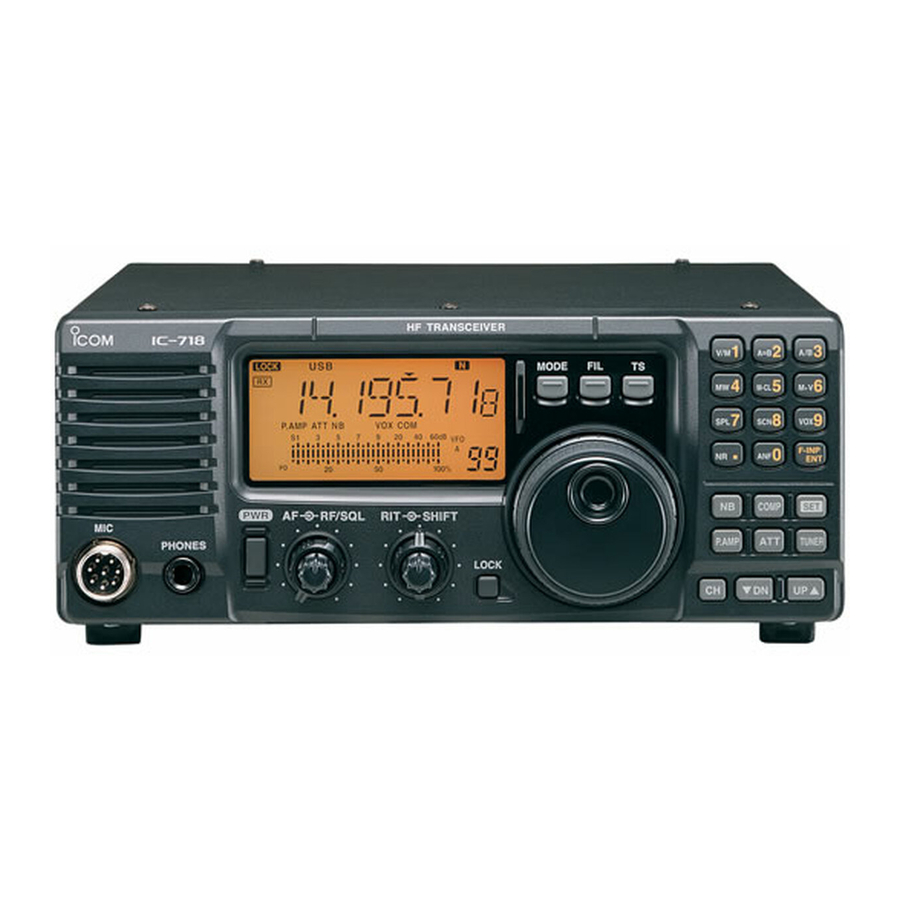
- Page 1 HF TRANCEIVER iC-718...
- Page 2 This service manual describes the latest service information NEVER connect the transceiver to an AC outlet or to a DC for the IC-718 HF TRANCEIVER at the time of publication. power supply that uses more than 16 V. This will ruin the transceiver.
-
Page 3: Table Of Contents
TABLE OF CONTENTS SECTION 1 SPECIFICATIONS SECTION 2 INSIDE VIEWS SECTION 3 DISASSEMBLY INSTRUCTIONS SECTION 4 CIRCUIT DESCRIPTION 4 – 1 RECEIVER CIRCUITS ........................4 – 1 4 – 2 TRANSMITTER CIRCUITS ......................4 – 4 4 – 3 PLL CIRCUIT ..........................4 – 5 4 –... -
Page 4: Specifications
SECTION 1 SPECIFICATIONS GENERAL RECEIVER • Frequency coverage • Receive system : Double-conversion Receive 0.030–29.999999 MHz* superheterodyne Transmit 1.800–1.999 MHz* 3.500–3.999 MHz* • Sensitivity (10 dB S/N) 7.000–7.300 MHz 10.100–10.150 MHz SSB, CW, RTTY 0.16 µV* (1.8–29.999999 MHz) 14.000–14.350 MHz 18.068–18.168 MHz 13 µV (0.5–1.799999 MHz) 21.000–21.450 MHz 24.890–24.990 MHz 2.0 µV*... -
Page 5: Inside Views
SECTION 2 INSIDE VIEWS ¡Top view (PA AND FILTER UNITS) PA unit Filter unit Predrive amplifier (Q1: 2SC1971) Tx/Rx switching relay (RL13: AG201344) SWR detector Drive amplifier (L13: LR-391) (Q2, Q3: 2SC3133) Power amplifier (Q4, Q5: 2SC2904) Tx low-pass filters (L13: LR-391) ¡Bottom view (MAIN AND PLL UNITS) 2nd mixer circuit... -
Page 6: Disassembly Instructions
SECTION 3 DISASSEMBLY INSTRUCTIONS • Removing the covers • How to connect the coaxial cable Remove 14 screws from the top and bottom covers. Connect the coaxial cable as shown in below. J701 to MAIN unit PA unit FILTER unit •... -
Page 7: Circuit Description
SECTION 4 CIRCUIT DESCRIPTION 4-1 RECEIVER CIRCUITS (3) 2.0–30.0 MHz The signals pass through a high pass filter (L811–L814, 4-1-1 RF SWITCHING CIRCUIT C811–C817) to suppress excessively strong signals below (FILTER AND MAIN UNITS) 2.0 MHz, such as from broadcasting stations. The filtered The RF switching circuit leads receive signals to bandpass signals are applied to a low-pass filter and one of 5 band- filters from the antenna connector while receiving. -
Page 8: Pll Unit
2nd LO signal, and are then applied to the NB circuit. BFO (Beat Frequency Oscillator) frequency is used at the SSB/CW detector and the balanced modulator. The IC-718 • Exact 2nd IF frequency uses a DDS IC for the BFO circuit. -
Page 9: Logic Unit
4-1-10 SSB/CW DEMODULATOR CIRCUITS When the strong signal disappears, C1804 and R1809 release the AGC line voltage in CW or RTTY mode to obtain (MAIN UNIT) a fast AGC release time. While in SSB or AM mode, C1803, In SSB or CW mode, the 2nd IF signal from the IF amplifier C1805, R1808 and C1802, R1807 are connected in parallel (Q1601) is mixed with the BFO signal from the PLL unit at to obtain a appropriate AGC characteristics (middle or slow... -
Page 10: Transmitter Circuits
The ALC (Automatic Level Control) circuit controls the gain of IF amplifiers in order for the IC-718 to output a constant RF power set by the [RF PWR] control even when the sup- 4-2-4 IF AMPLIFIER (MAIN UNIT) plied voltage shifts, etc. -
Page 11: Pll Circuit
When the “FOR” voltage exceeds the “POCV” voltage, ALC While transmitting, PAT8 voltage is provided to MF1 via R30. bias voltage from IC1701c (pin 8) controls the IF amplifiers Thermistor R30 on the PA unit detects the temperature of (Q151, Q502). This adjusts the output power to the deter- Q4. -
Page 12: Logic Circuits
The memory channel information is stored in the EEPROM (IC2). 4-4 LOGIC CIRCUITS The Icom CI-V network system allows the IC-718 to be remotely controlled by a personal computer using an RS- 4-4-1 BAND SELECTION DATA (MAIN UNIT) 232C I/O port. -
Page 13: Adjustment Procedures
RF power meter the antenna connector. to [DC 13.8 V] DC power supply Ammeter to [EXT SP] Distortion meter Speaker • Microphone connector (Front panel view) IC-718 Audio generator Pin 1 Pin 7 Pin 6 Pin 5 5 - 1... -
Page 14: Pll Adjustments
5-2 PLL ADJUSTMENTS ADJUSTMENT MEASUREMENT POINT ADJUSTMENT ADJUSTMENT CONDITION VALUE UNIT LOCATION UNIT ADJUST Turn L6, L7 on the PLL unit to downside for REFERENCE • Display frequency: Any Connect a frequency presetting until the frequency counter reads FREQUENCY • Set C16 as illustration at below. counter check frequency. - Page 15 • PLL unit 2nd LO check point Reference frequency check point Reference OSC level adjustment Reference freauency Reference adjustment frequency pre-setting 1st LO 1st LO output level check point C165 VCO lock voltage adjustment 5 - 3...
-
Page 16: Transmitter Adjustments
5-3 TRANSMITTER ADJUSTMENTS ADJUSTMENT MEASUREMENT POINT ADJUSTMENT ADJUSTMENT CONDITION VALUE UNIT LOCATION UNIT ADJUST IDLING • Display frequency: 14.10000 MHz Connect an ammeter At the point where the CURRENT • Mode : USB (3 A) between power Tx current Increases •... - Page 17 • PA unit • FILTER unit SWR detector check point Idling current adjustment SWR detector (Driver) pre-setting SWR detector Idling current adjustment adjustment (Final) • MAIN unit CP4002 Ic APC pre-setting L106 L151 L301 L302 Tx total gain L303 adjustment L501 R503 J3601...
- Page 18 TRANSMITTER ADJUSTMENTS—continued ADJUSTMENT MEASUREMENT POINT ADJUSTMENT ADJUSTMENT CONDITION VALUE UNIT LOCATION UNIT ADJUST CARRIER • Display frequency: 14.10000 MHz Rear Connect a spectrum Minimum carrier level MAIN R2303 SUPPRESSION • Mode : USB panel analyzer to the [ANT] • Mic gain : Minimum (0) connector through an •...
- Page 19 • MAIN unit CP3701 CW carrier check point R2303 Carrier suppression adjustment R2321 AM modulation adjustment R3703 (or AM carrier pre-setting) CW carrier adjustment R2385 AM carrier and R1730 AM modulation AM carrier pre-setting adjustment 5 - 7...
-
Page 20: Receiver Adjustments
5-4 RECEIVER ADJUSTMENTS Receiver total gain adjustment must perform after transmitter total gain adjustment. ADJUSTMENT MEASUREMENT POINT ADJUSTMENT ADJUSTMENT CONDITION VALUE UNIT LOCATION UNIT ADJUST RECEIVER • R2701 (MAIN unit): Center Rear Connect an AC milli- Maximum audio output MAIN L1103, ˚... - Page 21 • MAIN unit L1103 L1201 L1202 L1502 Noise blanker adjustment L1501 Rx total gain adjustment CP1501 Noise blanker check point L1621 L1614 R2701 Rx total gain pre-setting 5 - 9...
-
Page 22: Set Mode Adjustment
5-5 SET MODE ADJUSTMENT ADJUSTMENT ADJUSTMENT CONDITION DISPLAY OPERATION • Enter set mode adjustment for RX: Push [SET] key to enter the RX set- ENTERING ting. SET MODE 1 Turn power OFF. ADJUSTMENT 2 Terminate the [REMOTE] jack with a Or push [UP] key to skip the set FOR RX 3.5(d) mm mini-plug. - Page 23 SET MODE ADJUSTMENT —continued ADJUSTMENT ADJUSTMENT CONDITION DISPLAY OPERATION • Connect a 50 Ω dummy load or power Transmit using an external PTT SWR METER meter to [ANT] connector. switch to set SWR reference level after pushing [SET]. • Connect a 100 Ω dummy load or power Transmit using an external PTT meter to [ANT] connector.
-
Page 24: Front Unit
OPC-885 8900008930 CABLE OPC-885 6050009870 S.XTAL CR-567 (9.8304 MHz) 8900006990 CABLE OPC-683 6200001830 S.COIL NL 322522T-100J 8970023640 E.OTHER SX2242 ICOM SHIELD (1)/FR 6200001830 S.COIL NL 322522T-100J 6200003260 S.COIL NL 322522T-101J 6200002040 S.COIL NL 252018T-101J 6910012480 E.OTHER RMS20-250-201-1R 6200002040 S.COIL NL 252018T-101J 6450001230 E.OTHER... -
Page 25: Logic Board
[LOGIC BOARD] [LOGIC BOARD] ORDER ORDER DESCRIPTION DESCRIPTION 7030003560 S.RESISTOR ERJ3GEYJ 103 V (10 kΩ) R197 7030003480 S.RESISTOR ERJ3GEYJ 222 V (2.2 kΩ) 7030003480 S.RESISTOR ERJ3GEYJ 222 V (2.2 kΩ) R198 7030003480 S.RESISTOR ERJ3GEYJ 222 V (2.2 kΩ) ERJ3GEYJ 821 V (820 Ω) 7030003480 S.RESISTOR ERJ3GEYJ 222 V (2.2 kΩ) R199... -
Page 26: Main Unit
[LOGIC BOARD] [MAIN UNIT] ORDER ORDER DESCRIPTION DESCRIPTION 0910052055 PCB B 5382E 1110004080 S.IC µPC2709T-E3 6910012350 S.BEAD MMZ1608Y 102BT IC1701 1110003870 S.IC NJM2058M-T1 EP40 6910012350 S.BEAD MMZ1608Y 102BT IC1751 1110002700 S.IC NJM2904M-T1 EP45 6910012350 S.BEAD MMZ1608Y 102BT IC2001 1110004870 S.IC TA4101F (TE12L) EP46 6910012350 S.BEAD... - Page 27 [MAIN UNIT] [MAIN UNIT] ORDER ORDER DESCRIPTION DESCRIPTION D304 1790000620 S.DIODE MA77 (TX) L106 6150004270 COIL LS-483A (C-14924) D305 1790000620 S.DIODE MA77 (TX) L151 6150004280 COIL LS-484B (C-14927) D306 1790000620 S.DIODE MA77 (TX) L152 6200003260 S.COIL NL 322522T-101J D401 1750000430 S.DIODE HSB88WSTR L153 6200003550 S.COIL...
- Page 28 [MAIN UNIT] [MAIN UNIT] ORDER ORDER DESCRIPTION DESCRIPTION L3502 6180000960 COIL LAL 03NA 102K R633 7030003440 S.RESISTOR ERJ3GEYJ 102 V (1 kΩ) ERJ3GEYJ 101 V (100 Ω) L4501 6200003950 S.COIL HF50ACC 322513-T R634 7030003320 S.RESISTOR L4651 6200003950 S.COIL HF50ACC 322513-T R635 7030003560 S.RESISTOR ERJ3GEYJ 103 V (10 kΩ)
- Page 29 [MAIN UNIT] [MAIN UNIT] ORDER ORDER DESCRIPTION DESCRIPTION R1523 7030003640 S.RESISTOR ERJ3GEYJ 473 V (47 kΩ) R2105 7030003640 S.RESISTOR ERJ3GEYJ 473 V (47 kΩ) ERJ3GEYJ 470 V (47 Ω) R1601 7030003280 S.RESISTOR R2106 7030003640 S.RESISTOR ERJ3GEYJ 473 V (47 kΩ) ERJ3GEYJ 471 V (470 Ω) R1602 7030003400 S.RESISTOR...
- Page 30 [MAIN UNIT] [MAIN UNIT] ORDER ORDER DESCRIPTION DESCRIPTION ERJ3GEYJ 471 V (470 Ω) R2901 7030003400 S.RESISTOR C106 4030008650 S.CERAMIC C1608 JB 1H 332K-T-A ERJ3GEYJ 4R7 V (4.7 Ω) R2902 7030004040 S.RESISTOR C107 4030008470 S.CERAMIC C1608 JB 1H 272K-T-A R3001 7030003640 S.RESISTOR ERJ3GEYJ 473 V (47 kΩ) C108 4030011600 S.CERAMIC...
- Page 31 [MAIN UNIT] [MAIN UNIT] ORDER ORDER DESCRIPTION DESCRIPTION C851 4030011600 S.CERAMIC C1608 JB 1C 104KT-N C1511 4030011340 S.CERAMIC C1608 CH 1H 471J-T-A C852 4030011340 S.CERAMIC C1608 CH 1H 471J-T-A C1512 4510004440 S.ELECTROLYTIC ECEV1HA010SR C853 4030007110 S.CERAMIC C1608 CH 1H 680J-T-A C1513 4510004640 S.ELECTROLYTIC ECEV1CA470SP C854...
- Page 32 [MAIN UNIT] [MAIN UNIT] ORDER ORDER DESCRIPTION DESCRIPTION C2314 4030011600 S.CERAMIC C1608 JB 1C 104KT-N C4107 4030006880 S.CERAMIC C1608 JB 1H 472K-T-A C2315 4510005810 S.ELECTROLYTIC ECEV1HAR47R C4200 4030006880 S.CERAMIC C1608 JB 1H 472K-T-A C2352 4030006870 S.CERAMIC C1608 JB 1H 222K-T-A C4201 4030007090 S.CERAMIC C1608 CH 1H 470J-T-A...
- Page 33 ERJ3GEYJ 101 V (100 Ω) 7030003320 S.RESISTOR 7030003480 S.RESISTOR ERJ3GEYJ 222 V (2.2 kΩ) ERJ3GEYJ 471 V (470 Ω) 8970023610 E.OTHER SX2242 ICOM SHIELD (1)/MA 7030003400 S.RESISTOR ERJ3GEYJ 101 V (100 Ω) 8970023660 E.OTHER SX2242 J LEAD SET (2)/MA 7030003320 S.RESISTOR 7030003560 S.RESISTOR...
- Page 34 [PLL UNIT] [PLL UNIT] ORDER ORDER DESCRIPTION DESCRIPTION R105 7030003640 S.RESISTOR ERJ3GEYJ 473 V (47 kΩ) 4030006880 S.CERAMIC C1608 JB 1H 472K-T-A R106 7030003640 S.RESISTOR ERJ3GEYJ 473 V (47 kΩ) 4030006880 S.CERAMIC C1608 JB 1H 472K-T-A R107 7030003640 S.RESISTOR ERJ3GEYJ 473 V (47 kΩ) 4030006880 S.CERAMIC C1608 JB 1H 472K-T-A R108...
- Page 35 ERJ3GEYJ 4R7 V (4.7 Ω) 7030004040 S.RESISTOR ERJ3GEYJ 681 V (680 Ω) 8970023621 E.OTHER SX2242 0.8D COAXIAL TUBE (2)/PL 7030003420 S.RESISTOR 8970023630 E.OTHER SX2242 ICOM SHIELD (1)/PL 7510000130 THERMISTOR ERT-D2FHL 333S 7030003470 S.RESISTOR ERJ3GEYJ 182 V (1.8 kΩ) ERJ1WYJ100U (10 Ω) 7030006130 S.RESISTOR ERJ1WYJ100U (10 Ω)
-
Page 36: Filter Unit
[PA UNIT] [FILTER UNIT] ORDER ORDER DESCRIPTION DESCRIPTION 4030004740 S.CERAMIC C2012 JB 1H 472K-T-A L100 6200005050 S.COIL NL 252018T-330J [EUR], [ITA], [FRA], [ESP] L101 6200005050 S.COIL NL 252018T-330J 4030005140 S.CERAMIC C3216 JB 1E 104K-T-A L102 6200005010 S.COIL NL 252018T-100J [EUR], [ITA], [FRA], [ESP] L103 6200005050 S.COIL NL 252018T-330J... - Page 37 4010005930 CERAMIC HM11SJ SL 391J 500V 4010005930 CERAMIC HM11SJ SL 391J 500V 4030006880 S.CERAMIC C1608 JB 1H 472K-T-A 2710000520 FAN SB0812H-ICOM-00 4030006880 S.CERAMIC C1608 JB 1H 472K-T-A 4030006880 S.CERAMIC C1608 JB 1H 472K-T-A 4030006880 S.CERAMIC C1608 JB 1H 472K-T-A 8900009501 CABLE OPC-939A 4030006880 S.CERAMIC...
- Page 38 QTY. REF NO. DESCRIPTION QTY. 6510000370 ANT connector MR-DS 2510000670 Speaker VS-50-0827 2710000520 Fan SB0812H-ICOM-00 6910012480 Sensor RMS20-250-201-1R 6450001230 Snap plate HLJ0999-01-480 8930021010 Domed plug DP-500 6910000310 B312D insulation washer 8210016660 2241 front panel (A) 6910000340 P101 KD insulation sheet...
- Page 39 MP22 (C) MP14 (C) MP14 (C) MP22 (C) MP20 (C) MP20 (C) MP2 (C) EP2 (C) EP3 (C) MP20 (C) MP15 (C) MP20 (C) MP1 (L) MP22 (C) MP3 (L) MP22 (C) EP70 (L) MP26 (C) PA UNIT MP22 (C) MP23 (F) FILTER UNIT MP2 (L)
- Page 40 SECTION SECTION 8 PARTS LIST SEMI-CONDUCTOR INFORMATIONS 8-1 TRANSISTORS 8-2 DIODES NAME SYMBOL INSIDE VIEW NAME SYMBOL INSIDE VIEW NAME SYMBOL INSIDE VIEW NAME SYMBOL INSIDE VIEW 2SA1576A R 1SS184 2SK882-GR MA29B DAN202K 2SC1971 None 2SC3133 None 1SS226 2SK2171-4 1SS375-TL MA77 DA221 TL 2SC2714-O...
- Page 41 SECTION 9 BOARD LAYOUTS 9-1 MAIN UNIT The combination of this page and the next page shows the unit layout in the same configuration as the actual • TOP VIEW J4651 P.C. Board. to FILTER unit J1 to PA unit J6 to FILTER unit J3 SEND T13V...
- Page 42 9-2 PLL UNIT • TOP VIEW 2nd LO to MAIN unit J401 to MAIN unit J2001 BFOE 2LOE The combination of this page and the previous page shows the unit layout in the same configuration as the actual P.C. Board. MAIN UNIT •...
- Page 43 The combination of this page and the next page shows 9-3 LOGIC BOARD the unit layout in the same configuration as the actual • TOP VIEW P.C. Board. 9-4 PHONE BOARD 9-5 MIC BOARD 9-6 VR BOARD • TOP VIEW •...
- Page 44 The combination of this page and the previous page LOGIC UNIT shows the unit layout in the same configuration as the • BOTTOM VIEW actual P.C. Board. SEN2 SENSOR SEN1 SQLS SEND MICE to MIC board J2 to VR board J1 ESPO ESPO ESPO...
- Page 45 The combination of this page and the next page shows 9-7 FILTER UNIT the unit layout in the same configuration as the actual • TOP VIEW P.C. Board. to MAIN unit J701 to PA unit J7 CHASSIS CHASSIS 2 4 6 8 10 1 3 5 7 9 ANTENNA to LOGIC unit J4001...
- Page 46 The combination of this page and the previous page FILTER UNIT shows the unit layout in the same configuration as the • BOTTOM VIEW actual P.C. Board. 9 - 6...
- Page 47 9-8 PA UNIT to MAIN unit J4101 • TOP VIEW to FILTER unit J2 to MAIN unit J1 VARISTOR BOARD CHASSIS CHASSIS BROWN ORANGE STAR YELLOW BLACK BLACK The combination of this page and the next page shows the unit layout in the same configuration as the actual P.C.
- Page 48 PA UNIT • BOTTOM VIEW The combination of this page and the previous page VARISTOR BOARD shows the unit layout in the same configuration as the actual P.C. Board. 9 - 8...
-
Page 49: Block Diagram
SECTION 10 BLOCK DIAGRAM below 1.6 M Q1508 2SC4081 Q1509 DTA114 GATE IC2101A IC2701 CTRL 1.6–2 M OPTION M5282FP NJM2058 D1501 Q1503 Q1502 Q1501 AFGV 2SK882 2SK882 2SK882 1SS375 UT-102 UT-102 Q1506 Q1507 SIDE TONE/BEEP DTC114 2SC4081 NOISE NOISE NOISE 2–4 M MAIN UNIT LEVEL... -
Page 50: Wiring Diagram
SECTION 11 WIRING DIAGRAM CHASSIS FRONT UNIT LOGIC J4401 STRT STRT UNIT SNDS SNDS J4101 FSKK FSKK STAR MICE MICE SEND SEND SENSOR SQLS SQLS SEND SEND PA UNIT SEND SEND PAT8 PAT8 SEND SEND ASC2 SEN1 SEN1 PHOE PHOE SEN2 STAR STAR... -
Page 51: Voltage Diagrams
SECTION 12 VOLTAGE DIAGRAM CHASSIS PLL unit J4 PLL unit J1 – 1LOE 2LOE SB0812H-ICOM-00 12-1 FILTER, PA and MAIN unit J3601 1st Lo 2nd Lo J201 J401 Tx: 0V C511 Q511 AM ON: 0.6V AM ON: 0.6V Rx: 3.5V DTC114EE except AM: 3.4V... -
Page 52: Pll Unit
7.9V 3.2V 10µH R191 180 L40 100µH : 6.0V : 8.1V 3.9V Lo : 5.6V 2SD1619 T Lo : 11.0V C194 0.0047 OFF: 4.4V OFF: 13.0V 10µH LW-25 470p 10µH 2SC4081 R C106 C109 2.0V 1.3V 0.0047 0.0047 0.82µH DS70 DS73 DS76 DS79... - Page 53 6-9-16, Kamihigashi, Hirano-ku, Osaka 547-0002, Japan Phone : 06 6793 5302 : 06 6793 0013 : http://www.icom.co.jp/world/index.html < > Corporate Headquarters Communication Equipment 2380 116th Avenue N.E., Bellevue, WA 98004, U.S.A. Himmelgeister Str. 100, D-40225 Düsseldorf, Germany Phone : ( 425 ) 454-8155...
- Page 54 Count on us! S-13701MZ-C1 6-9-16, Kamihigashi, Hirano-ku, Osaka 547-0002, Japan © 2000 Icom Inc.
Need help?
Do you have a question about the IC-718 and is the answer not in the manual?
Questions and answers