Table of Contents
Advertisement
CONTENTS
PC boards shown are viewed from parts side.
The parts with no reference number or no parts number in the
exploded views are not supplied.
As regards the resistors and capacitors, refer to the circuit diagrams
contained in this manual.
£
must be replaced with identical components - refer to the appropriate
Parts of [ ] mark can be used only with the version designated.
Effective : December, 2002
SERVICE MANUAL
C C R R - - L L 6 6 0 0 0 0
2
3
6
18
22
27
£
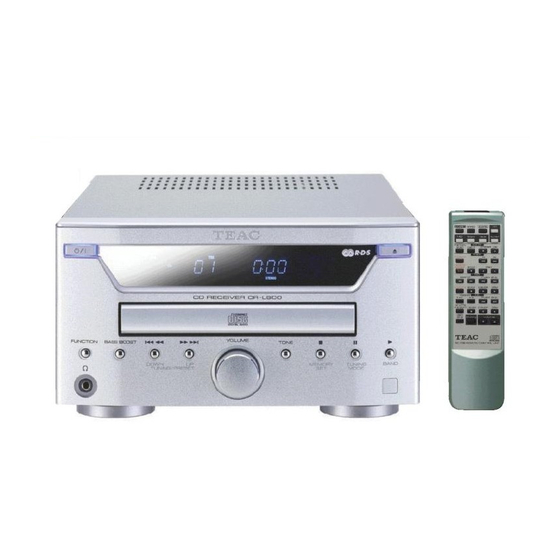
CD Receiver
Advertisement
Table of Contents

Subscribe to Our Youtube Channel
Related Manuals for Teac CR-L600


Summary of Contents for Teac CR-L600
-
Page 1: Table Of Contents
SERVICE MANUAL C C R R - - L L 6 6 0 0 0 0 CD Receiver CONTENTS 1 SPECIFICATIONS 2 ADJUSTMENTS AND CHECKS 3 IC BLOCK DIAGRAMS AND PIN FUNCTIONS 4 EXPLODED VIEWS AND PARTS LIST 5 PC BOARDS AND PARTS LIST 6 INCLUDED ACCESSORIES NOTES PC boards shown are viewed from parts side. -
Page 2: Specifications
1 SPECIFICATIONS AMPLIFIER Section Output Power ......30 W/ch (6 ohms, 0.5 %,1 kHz) Input Sensitivity..........350 mV/47k ohms Frequency Response ...... 20 Hz to 20,000 Hz (+1/-3 dB) TUNER Section FM Section Frequency Range ..87.50 MHz to 108.00 MHz (50 kHz steps) Signal-to-Noise Ratio .... -
Page 3: Adjustments And Checks
2 ADJUSTMENTS AND CHECKS... -
Page 6: Ic Block Diagrams And Pin Functions
3 IC BLOCK DIAGRAMS AND PIN FUNCTIONS TMP87PS71AF (IC31) I PIN ASSIGNMENTS (TOP VIEW) 54 53 52 51 50 49 48 47 46 45 44 43 42 41 (SIS) P97 P66 (G9) P65 (G10) (KEY0) P40 P64 (G11) (KEY1) P41 P63 (G12) (KEY2) P42 P62 (G13) - Page 7 PIN NO. SYMBOL DESCRIPTION F_MUTE FUNCTION MUTE CONTROL PORT REMO REMOTE CONTROL SENSOR DATA INPUT RDS CLK RDS CLOCK/DATA PORT RDS DATA V_SDATA VOL.IC CONTROL PORT V_SCLK CD_M_STBY CD STAND-BY PORT VSW2 VOLUME CONTROL PORT VSW1 RESET RESET INPUT PORT X_IN CRYSTAL CONNECTION PORT X_OUT...
-
Page 8: Block Diagram
NJW1136 (IC24) I BLOCK DIAGRAM TONE TONE TONE TONE AGC1 AGC1 SS-FIL SS-FIL LF1 LF2 LF3 LF1 LF2 LF3 OUTa OUTa SCL SDA AD SCL SDA AD VOL1 VOL1 IN a IN a TONE TONE VOL2 VOL2 NJRC NJRC I2C BUS I2C BUS Original Original... - Page 9 TA2153FN (IC12) I BLOCK DIAGRAM 36 pF 10 kΩ 50 kΩ 15 kΩ SBAD 15 kΩ 3 pF 30 kΩ 10 kΩ 20 kΩ 60 kΩ 10 kΩ 10 pF 2VRO 20 kΩ 20 kΩ 20 kΩ 12 kΩ 3 STATE RFRP 12 kΩ...
- Page 10 TC9164AF I BLOCK DIAGRAM R-COM L-COM L-COM R-COM L-COM R-COM DATA SHIFT REGISTER TC9163AF (IC21) I BLOCK DIAGRAM R-COM L-COM L-COM R-COM L-COM R-COM DATA SHIFT REGISTER...
- Page 11 TC9462A (IC10) I BLOCK DIAGRAM RFGC TMAX TEBC TMAXS ZDET HSSW TESIO0 FLGA MONIT FLGB FLGC COFS FLGD SPDA SPCK SBSY SFSY DAT A DMOUT CLCK CKSE SBOK DACT TESIN MBOV TESIO1 DOUT AOUT LRCK EMPH UHSO TEST0...
- Page 12 Pin No. Symbol Functional Description Remarks TEST0 Tes t mode terminal. Normally, keep at open. With pull-up resistor. Playback speed mode flag output terminal. UHSO Playback Speed Normal 2 times 4 times UHSO Subcode Q data emphasis flag output terminal. EMPH Emphasis ON at “H”...
- Page 13 Pin No. Symbol Functional Description Remarks TMAX detection result output terminal. Selected by 3-state output. TMAXS command bit (TMPS). (P2V , PV TMAX detection result output terminal. Selected by command bit (TMPS). TMAX Detection TMAX Output 3-state output. TMAX Longer than fixed freq. “P2V ”...
- Page 14 Pin No. Symbol Functional Description Remarks External flag output terminal for internal signal. FLGA Can select signal from TEZC, FOON , FOK and RFZC by command. External flag output terminal for internal signal. FLGB Can select signal from DFCT , FOON , FMON and RFZC by command.
- Page 15 Pin No. Symbol Functional Description Remarks Digital GND terminal. BUCK Micon in terface clock input terminal Schmitt input Command and data sending/receiving chip enable signal input terminal. Schmitt input The bus line becomes active at "L"level. TEST4 Test mode selection terminal. With pull-up resistor Local test mode selection terminal With pull-up resistor...
- Page 16 TC2000 Audio Signal Processor Pin Descriptions Function Description BIASCAP Bandgap reference times two (typically 2.5VDC). Used to set the common mode voltage for the input op amps. This pin is not capable of driving external circuitry. 2, 6 FDBKP2, FDBKP1 Positive switching feedback.
- Page 17 TP2050 Power Stage Pin Descriptions Function Description GND-SUB Substrate ground 35,36 VccSign Signal positive supply Vcc1A Positive supply Vcc1B Positive supply Vcc2A Positive supply Vcc2B Positive supply GND1A Negative supply GND1B Negative supply GND2A Negative supply GND2B Negative supply 16,17 OUT1A Output half bridge 1A 10,11...
-
Page 18: Exploded Views And Parts List
4 EXPLODED VIEWS AND PARTS LIST EXPLODED VIEW-1... - Page 19 EXPLODED VIEW-1 £ £ £ £...
- Page 20 EXPLODED VIEW-2...
- Page 21 EXPLODED VIEW-2 (KSL-2130CCM)
-
Page 22: Pc Boards And Parts List
5 PC BOARDS AND PARTS LIST MAIN PCB... - Page 23 INPUT PCB CD PCB...
- Page 24 FRONT PCB PHONE JACK PCB AMP PCB...
- Page 25 MAIN PCB ASSY CD PCB ASSY (MAIN PCB+INPUT PCB) £ FRONT PCB ASSY (FRONT PCB+PHONE JACK PCB) £ £...
- Page 26 AMP PCB ASSY...
-
Page 27: Included Accessories
6 INCLUDED ACCESSORIES INCLUDED ACCESSORIES... - Page 28 CR-L600 BLOCK DIAGRAM C C R R - - L L 6 6 0 0 0 0 CD Receiver 1 st Issue; November 2002...
- Page 29 CR-L600 WIRING DIAGRAM C C R R - - L L 6 6 0 0 0 0 CD Receiver 1 st Issue; November 2002...
- Page 30 CR-L600 SCHEMATIC DIAGRAM INPUT PCB, MAIN PCB MAIN PCB INPUT PCB C C R R - - L L 6 6 0 0 0 0 CD Receiver 1 st Issue; November 2002...
- Page 31 CR-L600 SCHEMATIC DIAGRAM CD PCB CD PCB C C R R - - L L 6 6 0 0 0 0 CD Receiver 1 st Issue; November 2002...
- Page 32 CR-L600 SCHEMATIC DIAGRAM AMP PCB, FRONT PCB, PHONE JACK PCB AMP PCB PHONE JACK PCB C C R R - - L L 6 6 0 0 0 0 FRONT PCB CD Receiver 1 st Issue; November 2002...
-
Page 33: Notes
CR-L600 SCHEMATIC DIAGRAM SMPS PCB SMPS PCB [JPN] SMPS PCB [EUR/UK] C C R R - - L L 6 6 0 0 0 0 NOTES: INSTRUCTIONS FOR SERVICE PERSONNEL £Parts marked with this sign are safety critical components. £...
Need help?
Do you have a question about the CR-L600 and is the answer not in the manual?
Questions and answers