Advertisement
Quick Links
Introduction
The 8T49N240, 8T49N241 and 8T49N242 evaluation boards are designed to help the customer evaluate the 8T49N240i, 8T49N241, and
8T49N242 devices, respectively. For the sake of simplicity this User Guide refers to the 8T49N242i evaluation board though all
statements also apply to the 8T49N240 and 8T49N241 evaluation board. When the board is connected to a PC running IDT Timing
Commander™ Software through USB, the device can be configured and programmed to generate frequencies with best-in-class
performances.
Requirements
▪ PC Requirements:
— IDT Timing Commander Software Installed
— USB 2.0 or 3.0 interface
— Windows XP SP3 or later
— Processor: Minimum 1GHz
— Memory: Minimum 512MB, recommended 1GB
— Available Disk Space: Min 600MB (1.5GB, 64-bit), recommended 1GB (2GB 64-bit)
— Network access during installation if the .NET framework is not currently installed on the system
▪ Power Supply with 3.3V and 1000mA rating
▪ Four banana plug cables to connect the power supply to the board
Quick Start: Powering Up the Board
1. Set 3.3V supply current limit to 500mA.
2. Remove all output terminations.
3. Set Dip Switch selectors to the middle position.
4. Connect a cable from a PC to the USB port.
5. Connect VEE to the GND jack.
6. Connect 3.3V to Vcc_J, Vcca_J, and Vcco_J jacks.
7. Power on the Power Supply.
8. Press the Reset Button.
Once correct operation is verified, set the power supply limit for the number of outputs to be active.
The USB port must be powered by the PC in order to have the correct I
Default Power-Up Condition
The 8T49N241 and 8T49n242 boards ship with a 38.88MHz surface-mount crystal populated on the top of the board. The 8T49N240
board ships with a 49.152MHz crystal. If a different crystal frequency is needed, this part must be removed (for more information, see
Crystal
Interface).
All outputs should be off and the current should measure ~236mA with 3.3V on Vcc_J, Vcca_J, and Vcco_J.
When evaluating performance with the default hardware configuration, it is recommended that all active outputs be terminated 50ohms to
VEE by either terminator plugs or an instrument.
©2017 Integrated Device Technology, Inc.
8T49N24x Evaluation Board User Guide
2
C bus voltage levels.
1
June 6, 2017
Advertisement

Related Manuals for IDT 8T49N241


Summary of Contents for IDT 8T49N241
- Page 1 8T49N242 devices, respectively. For the sake of simplicity this User Guide refers to the 8T49N242i evaluation board though all statements also apply to the 8T49N240 and 8T49N241 evaluation board. When the board is connected to a PC running IDT Timing Commander™...
-
Page 2: Board Overview
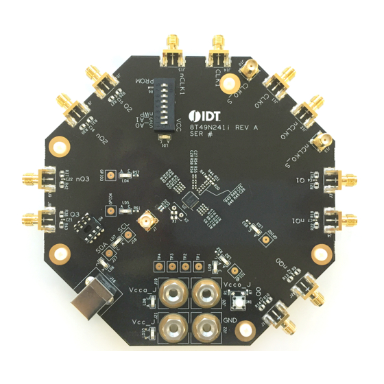
8T49N24x Evaluation Board User Guide Board Overview Use the following diagram to identify and locate: power supply jacks, USB connector, input and output SMA connectors, reset button, EEPROM, etc. Figure 1. Evaluation Board Overview ©2017 Integrated Device Technology, Inc. June 6, 2017... - Page 3 8T49N24x Evaluation Board User Guide Legend–Evaluation Board Inputs CLK0_S Clock 0 sense lines. CLK0 Clock 0 input lines. Can be configured for differential or single-ended input. CLK1 Clock 1 input lines. Can be configured for differential or single-ended input. Outputs Output Q0.
- Page 4 Software GUI Overview The 8T49N24x devices are programmed using IDT's Timing Commander software, which provides an interactive and intuitive Graphical User Interface to program and adjust the many settings that are available for the devices. Timing Commander is the generic platform upon which many devices' GUIs run on.
- Page 5 8T49N24x Evaluation Board User Guide Schematics The following figures are schematics that are applicable to specific sections of this User Guide. The complete schematics are available in a separate document. Figure 3. Inputs Schematic ©2017 Integrated Device Technology, Inc. June 6, 2017...
- Page 6 8T49N24x Evaluation Board User Guide Figure 4. Output Termination Schematic ©2017 Integrated Device Technology, Inc. June 6, 2017...
- Page 7 8T49N24x Evaluation Board User Guide Figure 5. Crystal Interface Schematic ©2017 Integrated Device Technology, Inc. June 6, 2017...
- Page 8 8T49N24x Evaluation Board User Guide Figure 6. EEPROM/I2C Schematic ©2017 Integrated Device Technology, Inc. June 6, 2017...
- Page 9 8T49N24x Evaluation Board User Guide Figure 7. DC Control Schematic Figure 8. GPIOs Schematic ©2017 Integrated Device Technology, Inc. June 6, 2017...
- Page 10 8T49N24x Evaluation Board User Guide Figure 9. VCCO Power Filtering Schematic ©2017 Integrated Device Technology, Inc. June 6, 2017...
- Page 11 8T49N24x Evaluation Board User Guide Figure 10. VCC Power Filtering Schematic ©2017 Integrated Device Technology, Inc. June 6, 2017...
- Page 12 8T49N24x Evaluation Board User Guide Figure 11. 8T49N241 and 8T49N242 DUT Schematic ©2017 Integrated Device Technology, Inc. June 6, 2017...
- Page 13 8T49N24x Evaluation Board User Guide Figure 12. 8T49N240 DUT Schematic ©2017 Integrated Device Technology, Inc. June 6, 2017...
- Page 14 8T49N24x Evaluation Board User Guide Board Power Supply Core Voltages The core voltage includes a digital supply voltage VCC and an analog supply voltage VCCA. The digital supply voltage is powered by an external bench power supply connected to J19 (VCCA_J). The analog supply voltage is powered by an external bench power supply connected to J21 (VCC_J) (see Figure Output Voltages...
-
Page 15: Input Configuration
8T49N24x Evaluation Board User Guide Input Configuration The inputs are configured with an AC-coupling termination scheme. This scheme allows flexibility for either differential or single-ended inputs. The default configuration is as follows: Table 1. Default Input Configuration Input Default Termination Sense Lines CLK0 Unterminated, AC-coupled into the device and terminated... -
Page 16: Output Configuration
8T49N24x Evaluation Board User Guide Output Configuration The outputs are AC-coupled, allowing for maximum flexibility for observation of the output whether configured for LVPECL, LVDS, LVCMOS, or HCSL levels. The default termination scheme can be used to measure any of the three output level-types but is not optimal. The optimal termination circuits are tabulated below. - Page 17 8T49N24x Evaluation Board User Guide Table 7. Spare Resistor Termination for LVPECL for Q0 Source resistors: 180ohm pull-down: Series capacitors: Spare Resistors: Signal Type R5, R8 R11, R12 C1,C2 R9, R10, R13, R14 LVPECL (Default) 0ohm Not Installed 0ohm R9=R10=125ohm R13=R14=84ohm HCSL 33ohm...
- Page 18 8T49N24x Evaluation Board User Guide Figure 14. EEPROM Programming To write to the EEPROM, make sure the I2C slave address is set to 0xA0 and the address type is set to “One Byte Addresses”, then click “Write to Alternate”. A confirmation message box will appear when the write is completed. DC Controls The DIP switch has three settings: 0V, Float, and VCC.
- Page 19 8T49N24x Evaluation Board User Guide Crystal Interface The board supports three types of crystals that can be used for the local reference oscillator of the device. If overdriving the crystal oscillator with an external signal, an optional extra connector must be attached to allow this. The board ships with a 38.88MHz surface-mount crystal populated in X1.
- Page 20 8T49N24x Evaluation Board User Guide Application Notes and Resources Design guidelines and resources may be found online for the 8T49N24x devices, at the following addresses: 8T49N240 http://www.idt.com/8T49N240 8T49N241 http://www.idt.com/8T49N241 8T49N242 http://www.idt.com/8T49N242 The site contains a wealth of information, including: ▪ Device datasheets and errata ▪...
-
Page 21: Revision History
IDT or any third parties. IDT's products are not intended for use in applications involving extreme environmental conditions or in life support systems or similar devices where the failure or malfunction of an IDT product can be rea- sonably expected to significantly affect the health or safety of users.
Need help?
Do you have a question about the 8T49N241 and is the answer not in the manual?
Questions and answers