Advertisement
Quick Links
82P33731/33831 Evaluation Board
Introduction
The 82P33731/33831 evaluation board is designed to help the customer evaluate the IDT82P33731 and IDT82P33831 devices.
This user guide will accomplish the following:
•
Introduce the board on its power supply and jumper settings
•
Describe the input and output connectors for normal operation
•
How to bring up the board by using Timing Commander software GUI
•
How to configure and program the board to generate standard-compliant frequencies
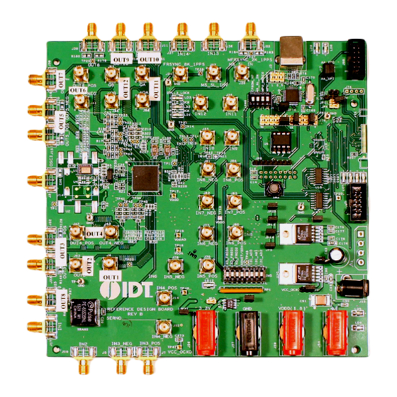
Board Overview
Use
Figure 1
to identify various components of the board: Input and output SMA connectors; Power supply jacks and some
jumper settings necessary for the board operations. Detailed descriptions are as follows:
•
Input SMA Connectors – There are a total of 14 inputs, of which IN1, 2 are AMI inputs; IN9, 10, 11, 12, 13, 14 are
single-ended inputs; IN3, 4, 5, 6, 7, 8 are differential inputs.
•
Output SMA Connectors – There are a total of 12 outputs, of which OUT1, 2, 7, 9, 10 are single-ended outputs; OUT3, 4, 5,
6, 11, 12 are differential outputs; OUT8 is an AMI output.
•
USB connector – Type-B connector for GUI communications. No power is drawn from USB connector other than to power
the FTDI USB chip.
•
Dip Switch SW6 – Used to configure EEPROM write protection, master or slave selection and communication protocols
between PC/GUI and the board. For typical I
•
J76 – This is a 2x12 pin header used to set communication mode between PC and the board.
header pairs for the intended mode. Use JP18 (described below) to set I
Table 1: Jumper Setting on J76
FTDI SPI
Aardvark SPI/I2C
3-4 Jumper
1-3 Jumper
9-10 Jumper
7-9 Jumper
15-16 Jumper
13-15 Jumper
21-22 Jumper
19-21 Jumper
•
2
JP18 – By default, I
C mode will be selected with JP18 shunted (jumped).
REVISION C 09/29/14
2
C mode, set MPU_MODE[1:0] = 00 ('I2C ON').
FTDI I2C
Motherboard SPI/I2C
3-4 Jumper
3-5 Jumper
9-10 Jumper
9-11 Jumper
14-16 Jumper
15-17 Jumper
21-23 Jumper
1
Table 1
2
C mode by default.
FTDI UART
4-6 Jumper
9-10 Jumper
15-16 Jumper
©2014 Integrated Device Technology, Inc.
USER GUIDE
shows how to jump the
FTDI to Aardvark
1-2 Jumper
7-8 Jumper
13-14 Jumper
19-20 Jumper
Advertisement

Related Manuals for IDT 82P33731


Summary of Contents for IDT 82P33731
-
Page 1: Board Overview
82P33731/33831 Evaluation Board USER GUIDE Introduction The 82P33731/33831 evaluation board is designed to help the customer evaluate the IDT82P33731 and IDT82P33831 devices. This user guide will accomplish the following: • Introduce the board on its power supply and jumper settings •... - Page 2 82P33731/33831 EVALUATION BOARD Figure 1. Board Overview • APLL3 Crystals – Crystals for APLL3 in the device. Three frequencies are supported – 24.8832MHz, 25MHz and 25.78125MHz – generating three different mode frequencies for SONET, Ethernet and Ethernet LAN, respectively. On the board, two crystals are installed and supported at the same time.
-
Page 3: Board Power Supply
82P33731/33831 EVALUATION BOARD • 5VDC Power Jack – If AC/DC power source is not used, a 5VDC power source can be plugged into the jack to power the board. Please note: Power Jacks labeled 3.3V and 1.8V are for other purposes. They can be left unused. -
Page 4: On-Board Crystal Installation
82P33731/33831 EVALUATION BOARD On-Board Crystal Installation Although three crystal frequencies (24.88320MHz, 25.00000MHz and 25.78125MHz) are supported for APLL3, only two crystals are installed on the board. Table 3 lists the crystals with different frequencies installed on two versions of 82P33x31 evaluation boards. - Page 5 82P33731/33831 EVALUATION BOARD Figure 3. Starting up Timing Commander GUI 3. After selecting “New Settings File”, a device selection window will pop up. In the window, choose the intended device in the list (82P33831 was selected in the following example). Click the button at the lower right corner of the window to browse and select the correct personality file, then click OK.
- Page 6 82P33731/33831 EVALUATION BOARD Figure 4. Select 82P33831 and Open personality file "IDT82P33x31_v1.0_TC_v1.5.1.2.tcp" 4. The GUI window with 82P33831 block diagram is open for configurations (Figure 5). Overall, the configuration window shows 14 inputs on the left and 12 outputs are on the right side of the window. In the center of the window, DPLL1~3 and APLL1~3 are displayed.
- Page 7 82P33731/33831 EVALUATION BOARD Figure 5. Top Configuration Window for 82P33831: Left – Input; Right – Output; Center – Device Block Diagram 5. For Input configuration, most frequencies can be entered for IN01 ~ IN14 and they will be automatically configured to be available to both DPLLs.
- Page 8 82P33731/33831 EVALUATION BOARD Figure 6. Enter input and Output Frequencies To associate an input clock (i.e., IN09) with a sync signal (such as 1PPS), click on the Input Buffer of IN09 (the triangle symbol following frequency entry box), a sub-configuration window for IN09 is shown below. In the window, IN10 is selected as sync signal.
- Page 9 82P33731/33831 EVALUATION BOARD Figure 7. IN10 is selected as Sync Signal for IN09 (green oval) If IN10 is only used as a sync signal for IN09, then disable IN10 to the DPLL as an input in the Input Buffer window of IN10, shown below.
- Page 10 82P33731/33831 EVALUATION BOARD ◦ G.8273.2: to configure the DPLL for T-BC (Telecom Boundary Clock), which occurs when a IEEE-1588 stack is directly controlling the DCO with phase offsets. It also puts the DPLL in combo mode to synchronize to the other PLL running G.8262-Option 1 profile...
- Page 11 82P33731/33831 EVALUATION BOARD Figure 10. DPLL Configuration Window - Operation Mode Settings In “Bandwidth and Damping” section, there are two options to select DPLL's bandwidth and damping factors during start, acquisition and locked phases: ◦ Always use Locked bandwidth/damping: this option will use the bandwidth and damping factor that are available when DPLL is locked;...
- Page 12 82P33731/33831 EVALUATION BOARD Figure 11. DPLL Configuration Window – Bandwidth/Damping Factor Settings 7. Output Configuration. Most output frequencies can be entered for OUT01~OUT12 and they will be automatically configured. However, 19.2MHz and 10MHz-based clocks are not supported by the default hardware profiles for the APLLs.
- Page 13 82P33731/33831 EVALUATION BOARD Figure 13. APLL1 Parameters for VCO = 614.4MHz ◦ To configure APLL2, select “(custom on DPLL1)” as shown in Figure 12. Then click on “Customize” button and ignore the initial Timing Commander error. Enter the values as shown in Figure 14 below.
- Page 14 82P33731/33831 EVALUATION BOARD Figure 15. Output Frequencies Entered after APLL1/APLL2 Configured (example) ◦ To configure APLL3, select the correct clock path and enter desired output frequencies in OUT11 and/or OUT12. Only OUT11 and OUT12 are from APLL3. Please see portion of the window configuring APLL3 in Figure 16 below.
- Page 15 82P33731/33831 EVALUATION BOARD ◦ Finally, FRSYNC & MRFRSYNC can be configured, if needed. Change FRSYNC & MFRSYNC to 1PPS. By default, the duty cycle of sync outputs is 50/50. If a pulse is desired, click on the applicable check box. The pulse width is based on OUT01 clock period.
- Page 16 82P33731/33831 EVALUATION BOARD Before making a USB/I2C connection to the board, all configurations discussed in Step 1~8 above are stored in GUI until the board is connected and configuration data are written to the device. Once the board is connected, by default, any changes to the GUI configurations will be instantaneously written to the respective registers unless this feature is turned off.
- Page 17 82P33731/33831 EVALUATION BOARD Figure 20. Opening Setting File and Personality File for Writing APLL3-related Register ◦ Once the same setting file and APLL-only personality file are selected, click on Open, a window for writing APLL3 will open, as shown below in Figure 21.
- Page 18 82P33731/33831 EVALUATION BOARD Figure 22. DPLL Status Window REVISION C 09/29/14...
-
Page 19: Board Schematics
82P33731/33831 EVALUATION BOARD Board Schematics Figure 23. 82P33x31 Evaluation Board Schematics - Page 1: Block Diagram REVISION C 09/29/14... - Page 20 82P33731/33831 EVALUATION BOARD Figure 24. 82P33x31 Evaluation Board Schematics - Page 2: Reference Selection REVISION C 09/29/14...
- Page 21 82P33731/33831 EVALUATION BOARD Figure 25. 82P33x31 Evaluation Board Schematics - Page 3: I/O Termination REVISION C 09/29/14...
- Page 22 82P33731/33831 EVALUATION BOARD Figure 26. 82P33x31 Evaluation Board Schematics - Page 4: Control REVISION C 09/29/14...
- Page 23 82P33731/33831 EVALUATION BOARD Figure 27. 82P33x31 Evaluation Board Schematics - Page 5: Power REVISION C 09/29/14...
- Page 24 IDT or any third parties. IDT’s products are not intended for use in applications involving extreme environmental conditions or in life support systems or similar devices where the failure or malfunction of an IDT product can be reasonably expected to significantly affect the health or safety of users.
Need help?
Do you have a question about the 82P33731 and is the answer not in the manual?
Questions and answers