Advertisement
Quick Links
NCN9252MUGEVB
High-Speed USB 2.0
(480 Mbps) DP3T Switch for
USB/UART/Data
Multiplexing Evaluation
Board User's Manual
OVERVIEW
The NCN9252 is a DP3T switch for combined UART and
USB 2.0 high−speed data applications. It allows portable
systems to use a single external port to transmit and receive
signals to and from three separate locations within the
portable system. It is comprised of two switches, each with
a single common I/O that alternates between three terminals.
They are operated together to allow three data sources, such
as a USB or UART transceiver, to pass differential data
through a shared USB connector port.
The NCN9252 features low RON− 4 W (max) at 4.2 V
, 5 W (typ) at a 3.3 V V
V
CC
© Semiconductor Components Industries, LLC, 2012
April, 2012 − Rev. 3
. It also features low CON,
CC
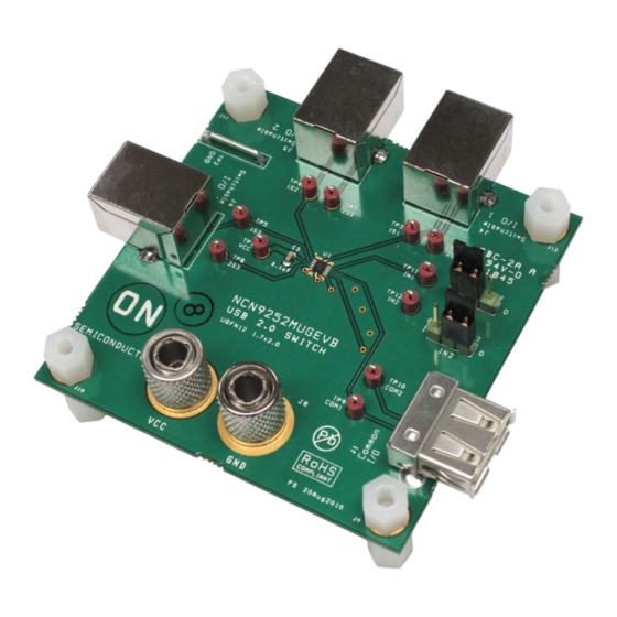
Figure 1. Board Photo
EVAL BOARD USER'S MANUAL
< 30 pF (max) across the supply voltage range. This
performance makes it ideal for both USB full−speed and
high*speed applications that require both low RON and
CON for effective signal transmission. The NCN9252 is
capable of accepting control input signals down to 1.4 V,
over a range of V
supply voltages with minimal leakage
CC
current. The NCN9252 is offered in a Pb−Free, 12 pin,
1.7 x 2.0 x 0.5 mm, UQFN package.
1
http://onsemi.com
Publication Order Number:
EVBUM2103/D
Advertisement

Related Manuals for ON Semiconductor NCN9252


Summary of Contents for ON Semiconductor NCN9252
- Page 1 1.7 x 2.0 x 0.5 mm, UQFN package. through a shared USB connector port. The NCN9252 features low RON− 4 W (max) at 4.2 V , 5 W (typ) at a 3.3 V V . It also features low CON, Figure 1.
- Page 2 NCN9252MUGEVB COM1 COM2 Control Logic Figure 2. Functional Block Diagram Table 1. FUNCTION TABLE IN1 [0] IN2 [1] COM1 Closed to: COM2 Closed to: No Connect No Connect Get Started... Equipment needed Procedure • 1. Set the power supply to 3.3 V. Connect the power Power Supply supply from V to GND using the banana cables.
- Page 3 J9, J10, J11, J13 Standoff screw Keystone Electronics 4814K−ND TP1, TP3, TP4, Test Point PC Multi Purpose 1mm hole Keystone Electronics 5000 TP5, TP6, TP7, TP8, TP9, TP10, TP11, TP12 PCB shorting link GND_Strap Harwin D3082−46 NCN9252 UQFN12 ON Semiconductor NCN9252MUTAG http://onsemi.com...
- Page 4 NCN9252MUGEVB PCB LAYOUT GUIDELINES Electrical Layout Considerations • Implementing a high speed USB device requires paying The ground plane of the PCB will be used to determine attention on USB lines and traces to preserve signal the characteristic impedance of each line. integrity.
- Page 5 onsemi, , and other names, marks, and brands are registered and/or common law trademarks of Semiconductor Components Industries, LLC dba “onsemi” or its affiliates and/or subsidiaries in the United States and/or other countries. onsemi owns the rights to a number of patents, trademarks, copyrights, trade secrets, and other intellectual property. A listing of onsemi’s product/patent coverage may be accessed at www.onsemi.com/site/pdf/Patent−Marking.pdf.
Need help?
Do you have a question about the NCN9252 and is the answer not in the manual?
Questions and answers