Advertisement
Quick Links
NCN1154MUTGEVB
NCN1154 DP3T USB 2.0
High Speed Audio Switch
Evaluation Board User's
Manual
Prepared by: Bertrand RENAUD
On Semiconductor
OVERVIEW
The NCN1154 is a DP3T switch for combined
true−ground audio, USB 2.0 high speed data, and UART
applications. It allows portable systems to use a single port
to pass either USB data or audio signals from an external
headset. The switch is capable of passing signals with
negative voltages as low as 2 V below ground.
The NCN1154 features shunt resistors on the audio ports.
These resistors are switched in when the audio channel is off
© Semiconductor Components Industries, LLC, 2010
July, 2010 − Rev. 0
and provide a safe path to ground for any charge that may
build up on the audio lines.
This reduces Pop & Click noise in the audio system. The
device has an extended V
V
up to 4.2 V while passing true ground audio signals
CC
down to −2 V.
The NCN1154 is housed in a space saving, ultra low
profile 1.7 x 2.0 x 0.5 mm 12 pin DFN package.
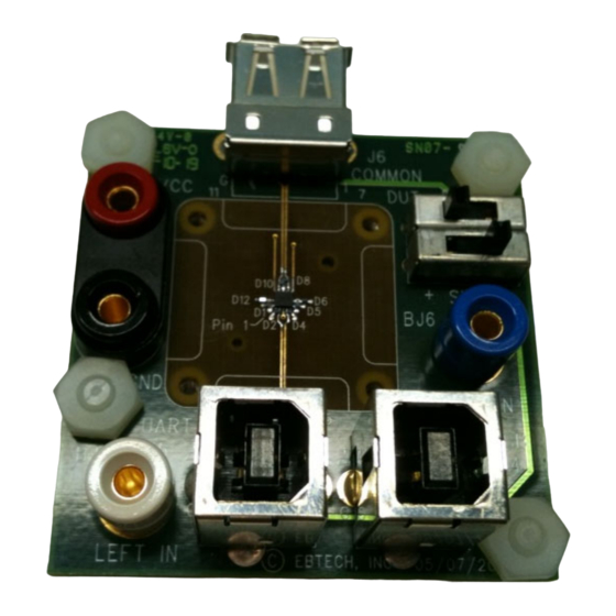
Figure 1. Board Picture
1
http://onsemi.com
EVAL BOARD USER'S MANUAL
range which can operate off
CC
Publication Order Number:
EVBUM2003/D
Advertisement

Subscribe to Our Youtube Channel
Related Manuals for ON Semiconductor NCN1154MUTGEVB


Summary of Contents for ON Semiconductor NCN1154MUTGEVB
- Page 1 NCN1154MUTGEVB NCN1154 DP3T USB 2.0 High Speed Audio Switch Evaluation Board User's Manual http://onsemi.com Prepared by: Bertrand RENAUD On Semiconductor EVAL BOARD USER’S MANUAL OVERVIEW The NCN1154 is a DP3T switch for combined and provide a safe path to ground for any charge that may true−ground audio, USB 2.0 high speed data, and UART...
- Page 2 NCN1154MUTGEVB NCN1154 − BOARD SCHEMATIC Figure 2. Board Schematic http://onsemi.com...
- Page 3 NCN1154MUTGEVB NCN1154 − BOARD CONNECTIONS SUPPLY Symbol Description VCC, GND This is the positive and the return connection for power supply (Pins 3 and 9). SETUP Symbol Description This is the toggle switch for IN2 (Pin 7). This is the toggle switch for IN1 (Pin 11).
- Page 4 NCN1154MUTGEVB NCN1154 − TEST PROCEDURE Equipment needed − Power Supply − Digital Ohm Meter − Desktop or Laptop with Windows XP or higher − USB Key − USB Headset BACKGROUND: IN1 & IN2 TRUTH TABLE D+, D− L, R L, R SHUNT...
- Page 5 NCN1154MUTGEVB NCN1154 − COMPONENTS SELECTION Input Capacitor A 0.1 mF X5R ceramic capacitor or larger must bypass Vcc input to the ground. This capacitor should be placed as close as possible to this input. ESD Diode These devices have limited built−in ESD protection, an external bi−directional ESD / IEC diode is recommended on COM+ and COM−...
- Page 6 NCN1154MUTGEVB NCN1154 − DEMOBOARD PCB LAYOUT Board Reference: EBT1745−01 REV: A Figure 3. Top Layer Routing http://onsemi.com...
- Page 7 NCN1154MUTGEVB Figure 4. Bottom Layer Routing http://onsemi.com...
-
Page 8: Technical Support
LIMITATIONS OF LIABILITY: ON Semiconductor shall not be liable for any special, consequential, incidental, indirect or punitive damages, including, but not limited to the costs of requalification, delay, loss of profits or goodwill, arising out of or in connection with the board, even if ON Semiconductor is advised of the possibility of such damages. In no event shall ON Semiconductor’s aggregate liability from any obligation arising out of or in connection with the board, under any theory of liability, exceed the purchase price paid for the board, if any. - Page 9 Mouser Electronics Authorized Distributor Click to View Pricing, Inventory, Delivery & Lifecycle Information: ON Semiconductor NCN1154MUTGEVB...
Need help?
Do you have a question about the NCN1154MUTGEVB and is the answer not in the manual?
Questions and answers