Table of Contents
Advertisement
Quick Links
Features
• Second-generation HOTLink
• Compliant to SMPTE 292M and SMPTE 259M video
standards
• Single channel video serializer plus single channel
video reclocking deserializer
— 195- to 1500-Mbps serial data signaling rate
— Simultaneous operation at different signaling rates
• Supports reception of either 1.485 or 1.485/1.001 Gbps
data rate with the same training clock
• Internal phase-locked loops (PLLs) with no external
PLL components
• Supports half-rate and full-rate clocking
• Selectable differential PECL-compatible serial inputs
— Internal DC-restoration
• Redundant differential PECL-compatible serial outputs
— No external bias resistors required
— Internal source termination
— Signaling-rate controlled edge-rates
• Synchronous LVTTL parallel interface
• JTAG boundary scan
• Built-In Self-Test (BIST) for at-speed link testing
• Link Quality Indicator
— Analog signal detect
— Digital signal detect
• Low-power 1.8W @ 3.3V typical
• Single 3.3V supply
• Thermally enhanced BGA
• Pb-Free package option available
• 0.25µ BiCMOS technology
Functional Description
The CYV15G0104TRB Independent Clock HOTLink II™
Serializer and Reclocking Deserializer is a point-to-point or
point-to-multipoint communications building block enabling
10
10
Cypress Semiconductor Corporation
Document #: 38-02100 Rev. *B
Independent Clock HOTLink II™ Serializer and
®
technology
Independent
Channel
CYV15G0104TRB
Device
Reclocked
Output
Figure 1. HOTLink II™ System Connections
•
3901 North First Street
Reclocking Deserializer
transfer of data over a variety of high-speed serial links
including SMPTE 292M and SMPTE 259M video applications.
It supports signaling rates in the range of 195 to 1500 Mbps
per serial link. The transmit and receive channels are
independent and can operate simultaneously at different
rates. The transmit channel accepts 10-bit parallel characters
in an Input Register and converts them to serial data. The
receive channel accepts serial data and converts it to 10-bit
parallel characters and presents these characters to an Output
Register. The received serial data can also be reclocked and
retransmitted through the reclocker serial outputs. Figure 1
illustrates typical connections between independent video co-
processors and corresponding CYV15G0104TRB chips.
The CYV15G0104TRB satisfies the SMPTE 259M and
SMPTE 292M compliance as per SMPTE EG34-1999 Patho-
logical Test Requirements.
As
a
second-generation
CYV15G0104TRB extends the HOTLink family with enhanced
levels of integration and faster data rates, while maintaining
serial-link compatibility (data and BIST) with other HOTLink
devices. The transmit (TX) channel of the CYV15G0104TRB
HOTLink II device accepts scrambled 10-bit transmission
characters. These characters are serialized and output from
dual Positive ECL (PECL) compatible differential trans-
mission-line drivers at a bit-rate of either 10- or 20-times the
input reference clock for that channel.
The receive (RX) channel of the CYV15G0104TRB HOTLink
II device accepts a serial bit-stream from one of two selectable
PECL-compatible differential line receivers, and using a
completely integrated Clock and Data Recovery PLL, recovers
the timing information necessary for data reconstruction. The
recovered bit-stream is reclocked and retransmitted through
the reclocker serial outputs. Also, the recovered serial data is
deserialized and presented to the destination host system.
The transmit and receive channels contain an independent
BIST pattern generator and checker, respectively. This BIST
hardware allows at-speed testing of the high-speed serial data
paths in each transmit and receive section, and across the
interconnecting links.
Reclocked
Output
Independent
Channel
Serial
CYV15G0104TRB
Links
Device
,
•
San Jose
CYV15G0104TRB
HOTLink
device,
10
10
CA 95134
•
408-943-2600
Revised July 8, 2005
the
[+] Feedback
Advertisement
Table of Contents

Subscribe to Our Youtube Channel
Related Manuals for Cypress Semiconductor HOTLink II CYV15G0104TRB


Summary of Contents for Cypress Semiconductor HOTLink II CYV15G0104TRB
- Page 1 II device accepts a serial bit-stream from one of two selectable PECL-compatible differential line receivers, and using a completely integrated Clock and Data Recovery PLL, recovers the timing information necessary for data reconstruction. The recovered bit-stream is reclocked and retransmitted through the reclocker serial outputs.
- Page 2 The CYV15G0104TRB is ideal for SMPTE applications where different data rates and serial interface standards are necessary for each channel. Some applications include multi- CYV15G0104TRB Serializer and Reclocking Deserializer Logic Block Diagram Document #: 38-02100 Rev. *B format routers, switchers, format converters, SDI monitors, cameras, and camera control units.
- Page 3 LDTDEN Receive Signal INSELA Monitor INA1+ INA1– Clock & INA2+ Recovery INA2– ULCA SPDSELA RXPLLPDA Recovered Character Clock RECLKOA Character-Rate Clock REPDOA Serializer Path Block Diagram REFCLKB+ REFCLKB– TXRATEB SPDSELB TXCLKOB TXERRB TXCLKB TXCKSELB TXDB[9:0] Device Configuration and Control Block Diagram...
-
Page 4: Pin Configuration (Top View)
Pin Configuration (Top View) TCLK RESET INSELA ULCA WREN DB[0] DB[1] DB[2] DB[9] DB[3] DB[4] DB[8] DB[5] DB[7] DB[6] CLKB Note: NC = Do not connect. Document #: 38-02100 Rev. *B TOUT TOUT ROUT B1– B2– A1– A1– TOUT TOUT ROUT DATA DATA... - Page 5 Pin Configuration (Bottom View) ROUT A2– ROUT TRST LDTD SELB TMEN3 SCAN SELA BIST DA[0] DA[4] DA[1] DA[2] DA[5] DA[9] LFIA DA[3] DA[6] CLKA+ DA[7] DA[8] CLKA– ERRB Document #: 38-02100 Rev. *B ROUT TOUT A2– A1– A1– B2– ROUT TOUT DATA DATA...
- Page 6 Reference Clock. REFCLKB± clock inputs are used as the timing reference for the or single-ended transmit PLL. This input clock may also be selected to clock the transmit parallel interface. LVTTL input clock When driven by a single-ended LVCMOS or LVTTL clock source, connect the clock source to either the true or complement REFCLKB input, and leave the alternate REFCLKB input open (floating).
- Page 7 LVTTL input clock time. In the presence of valid serial data, the recovered clock output of the receive CDR PLL (RXCLKA±) has no frequency or phase relationship with TRGCLKA±. When driven by a single-ended LVCMOS or LVTTL clock source, connect the clock source to either the true or complement TRGCLKA input, and leave the alternate TRGCLKA input open (floating).
- Page 8 Receive Input Selector. The INSELA input determines which external serial bit stream asynchronous is passed to the receiver’s Clock and Data Recovery circuit. When INSELA is HIGH, the Primary Differential Serial Data Input, INA1±, is selected for the receive channel. When INSELA is LOW, the Secondary Differential Serial Data Input, INA2±, is selected for the...
- Page 9 Internal Latch Reclocker Differential Serial Output Driver 1 Enable. PABRSTB Internal Latch Transmit Clock Phase Alignment Buffer Reset. Factory Test Modes SCANEN2 LVTTL input, Factory Test 2. SCANEN2 input is for factory testing only. This input may be left as a NO internal pull-down CONNECT, or GND only.
- Page 10 The Transmit PLL Clock Multiplier accepts a character-rate or half-character-rate external clock at the REFCLKB± input, and that clock is multiplied by 10 or 20 (as selected by TXRATEB) to generate a bit-rate clock for use by the transmit shifter. It also provides a character-rate clock used by the transmit paths, and outputs this character rate clock as TXCLKOB.
- Page 11 2 ms. Clock/Data Recovery The extraction of a bit-rate clock and recovery of bits from the received serial stream is performed by a separate CDR block within the receive channel. The clock extraction function is CYV15G0104TRB TRGCLKA±...
-
Page 12: Power Control
The receive channel performs a reclocker function on the incoming serial data. To do this, the Clock and Data Recovery PLL first recovers the clock from the data. The data is retimed by the recovered clock and then passed to an output register. - Page 13 Training Clock Rate Select. The initialization value of the TRGRATEA latch = 0. TRGRATEA is used to select the clock multiplier for the training clock input to the CDR PLL. When TRGRATEA = 0, the TRGCLKA± input is not multiplied before it is passed to the CDR PLL. When TRGRATEA = 1, the TRGCLKA± input is multiplied by 2 before it is passed to the CDR PLL.
- Page 14 Transmit PLL. When TXRATEB = 0, the transmit PLL multiples the REFCLKB± input by 10 to generate the serial bit-rate clock. When TXRATEB = 0, the TXCLKOB output clocks are full-rate clocks and follow the frequency and duty cycle of the REFCLKB± input. When TXRATEB = 1, the Transmit PLL multiplies the REFCLKB±...
-
Page 15: Jtag Support
This capability is present only on the LVTTL inputs and outputs, the TRGCLKA± input, and the REFCLKB± clock input. The high- speed serial inputs and outputs are not part of the JTAG test chain. - Page 16 CYV15G0104TRB Monitor Data Receive BIST Received Detected LOW {BISTSTA, RXDA[0], RX PLL RXDA[1]} = Out of Lock BIST_START (101) {BISTSTA, RXDA[0], RXDA[1]} = BIST_WAIT (111) Start of BIST Detected Yes, {BISTSTA, RXDA[0], RXDA[1]} = BIST_DATA_COMPARE (000, 001) Compare Next Character Mismatch {BISTSTA, RXDA[0], RXDA[1]} = Match...
-
Page 17: Maximum Ratings
Maximum Ratings (Above which the useful life may be impaired. User guidelines only, not tested.) Storage Temperature ... –65°C to +150°C Ambient Temperature with Power Applied... –55°C to +125°C Supply Voltage to Ground Potential ... –0.5V to +3.8V DC Voltage Applied to LVTTL Outputs in High-Z State ...–0.5V to V Output Current into LVTTL Outputs (LOW)...60 mA DC Input Voltage...–0.5V to V... - Page 18 0.8V 0.8V ≤ 1 ns (c) LVTTL Input Test Waveform CYV15G0104TRB AC Electrical Characteristics Parameter CYV15G0104TRB Transmitter LVTTL Switching Characteristics Over the Operating Range TXCLKB Clock Cycle Frequency TXCLKB Period=1/f TXCLK [16] TXCLKB HIGH Time TXCLKH [16] TXCLKB LOW Time...
- Page 19 17. The ratio of rise time to falling time must not vary by greater than 2:1. 18. For a given operating frequency, neither rise or fall specification can be greater than 20% of the clock-cycle period or the data sheet maximum time.
-
Page 20: Pll Characteristics
30%–70%. 24. TRGCLKA± has no phase or frequency relationship with the recovered clock(s) and only acts as a centering reference to reduce clock synchronization time. TRGCLKA± must be within ±1500 PPM (±0.15%) of the transmitter PLL reference (REFCLK±) frequency. Although transmitting to a HOTLink II receiver channel necessitates the frequency difference between the transmitter and receiver reference clocks to be within ±1500-PPM, the stability of the crystal needs to be... - Page 21 TXDB[ 9 :0] Note: 27. When REFCLKB± is configured for half-rate operation (TXRATEB = 1) and data is captured using REFCLKB instead of a TXCLKB clock. Data is captured using both the rising and falling edges of REFCLKB. Document #: 38-02100 Rev. *B...
- Page 22 CYV15G0104TRB HOTLink II Transmitter Switching Waveforms Transmit Interface TXCLKOB Timing TXRATE = 1 REFCLKB Note 29 TXCLKOB (internal) Transmit Interface TXCLKOB Timing TXRATEB = 0 REFCLKB Note29 TXCLKOB Switching Waveforms for the CYV15G0104TRB HOTLink II Receiver Receive Interface Read Timing RXRATEA = 0 RXCLKA+ RXCLKA–...
- Page 23 Switching Waveforms for the CYV15G0104TRB HOTLink II Receiver Receive Interface Read Timing RXRATEA = 1 RXCLKA+ RXCLKA– RXDA[9:0] Bus Configuration Write Timing ADDR[2:0] DATA[6:0] WREN Document #: 38-02100 Rev. *B RXCLKP RXDV– RXDV+ WRENP DATAS CYV15G0104TRB DATAH Page 23 of 27 [+] Feedback...
- Page 24 Table 7. Package Coordinate Signal Allocation Ball Signal Name Signal Type NO CONNECT NO CONNECT NO CONNECT NO CONNECT POWER NO CONNECT TOUTB1– CML OUT GROUND GROUND TOUTB2– CML OUT INA1– CML IN ROUTA1– CML OUT GROUND INA2– CML IN ROUTA2–...
- Page 25 Table 7. Package Coordinate Signal Allocation (continued) Ball Signal Name Signal Type POWER POWER NO CONNECT NO CONNECT NO CONNECT NO CONNECT NO CONNECT NO CONNECT GROUND GROUND GROUND GROUND GROUND GROUND GROUND GROUND GROUND NO CONNECT NO CONNECT NO CONNECT NO CONNECT GROUND GROUND...
-
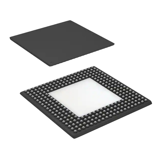
Page 26: Ordering Information
Ordering Information Speed Ordering Code Standard CYV15G0104TRB-BGC Standard CYV15G0104TRB-BGXC Package Diagram 256-Lead L2 Ball Grid Array (27 x 27 x 1.57 mm) BL256 HOTLink is a registered trademark and HOTLink II is a trademark of Cypress Semiconductor. All product and company names mentioned in this document may be the trademarks of their respective holders. - Page 27 Document History Page Document Title: CYV15G0104TRB Independent Clock HOTLink II™ Serializer and Reclocking Deserializer Document Number: 38-02100 ISSUE REV. ECN NO. DATE 244348 See ECN 338721 See ECN 384307 See ECN Document #: 38-02100 Rev. *B ORIG. OF CHANGE DESCRIPTION OF CHANGE...
Need help?
Do you have a question about the HOTLink II CYV15G0104TRB and is the answer not in the manual?
Questions and answers