Table of Contents
Advertisement
Quick Links
LM2596 SIMPLE SWITCHER
1 Features
•
New product available:
–
LMR51430 4.5 to 36-V, 3-A, 500-kHz and 1.1-
MHz synchronous converter
•
For faster time to market:
–
TLVM13630 3 to 36-V, 3-A, 200-kHz to 2.2-MHz
power module
•
3.3-V, 5-V, 12-V, and adjustable output versions
•
Adjustable version output voltage range: 1.2-V to
37-V ±4% maximum over line and load conditions
•
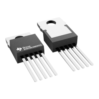
Available in TO-220 and TO-263 packages
•
3-A output load current
•
Input voltage range up to 40 V
•
Requires only four external components
•
Excellent line and load regulation specifications
•
150-kHz fixed-frequency internal oscillator
•
TTL shutdown capability
•
Low power standby mode, I
•
High efficiency
•
Uses readily available standard inductors
•
Thermal shutdown and current-limit protection
•
Create a custom design using the LM2596 with the
WEBENCH
®
Power Designer
2 Applications
•
Appliances
•
Grid infrastructure
•
EPOS
•
Home theater
(Fixed Output Voltage Versions)
An IMPORTANT NOTICE at the end of this data sheet addresses availability, warranty, changes, use in safety-critical applications,
intellectual property matters and other important disclaimers. PRODUCTION DATA.
3-A Step-Down Voltage Regulator
, typically 80 μA
Q
Typical Application
SNVS124G – NOVEMBER 1999 – REVISED MARCH 2023
®
Power Converter 150-kHz
3 Description
The LM2596 series of regulators are monolithic
integrated circuits that provide all the active functions
for a step-down (buck) switching regulator, capable
of driving a 3-A load with excellent line and load
regulation. These devices are available in fixed output
voltages of 3.3 V, 5 V, 12 V, and an adjustable output
version.
Requiring
a
minimum
components, these regulators are simple to use and
include internal frequency compensation, and a fixed-
frequency oscillator.
The LM2596 series operates at a switching frequency
of 150 kHz, thus allowing smaller sized filter
components
than
what
lower frequency switching regulators. Available in a
standard 5-pin TO-220 package with several different
lead bend options, and a 5-pin TO-263 surface mount
package.
Package Information
PART NUMBER
PACKAGE
NDH (TO-220, 5) 14.986 mm × 10.16 mm
LM2596
KTT (TO-263, 5) 10.10 mm × 8.89 mm
(1)
For all available packages, see the orderable addendum at
the end of the data sheet.
LM2596
number
of
external
can
be
required
with
(1)
BODY SIZE (NOM)
Advertisement
Table of Contents

Related Manuals for Texas Instruments SIMPLE SWITCHER LM2596


Summary of Contents for Texas Instruments SIMPLE SWITCHER LM2596
-
Page 1: Features
LM2596 SNVS124G – NOVEMBER 1999 – REVISED MARCH 2023 ® LM2596 SIMPLE SWITCHER Power Converter 150-kHz 3-A Step-Down Voltage Regulator 1 Features 3 Description • New product available: The LM2596 series of regulators are monolithic integrated circuits that provide all the active functions –... -
Page 2: Table Of Contents
Removed all references to design software Switchers Made Simple ..............Changes from Revision B (April 2013) to Revision C (April 2013) Page • Changed layout of National Semiconductor Data Sheet to TI format............... Submit Document Feedback Copyright © 2023 Texas Instruments Incorporated Product Folder Links: LM2596... -
Page 3: Description (Continued)
±15% on the oscillator frequency. External shutdown is included, featuring typically 80 μA standby current. Self-protection features include a two stage frequency reducing current limit for the output switch and an overtemperature shutdown for complete protection under fault conditions. Copyright © 2023 Texas Instruments Incorporated Submit Document Feedback Product Folder Links:... -
Page 4: Pin Configuration And Functions
ON/OFF pin can be wired to the ground pin or it can be left open. In either case, the regulator will be in the ON condition. Submit Document Feedback Copyright © 2023 Texas Instruments Incorporated Product Folder Links: LM2596... -
Page 5: Specifications
Recommended Operating Conditions. Exposure to absolute-maximum-rated conditions for extended periods may affect device reliability. If Military/Aerospace specified devices are required, please contact the Texas Instruments Sales Office/ Distributors for availability and specifications. Voltage internally clamped. If clamp voltage is exceeded, limit current to a maximum of 1 mA. -
Page 6: Electrical Characteristics - 3.3-V Version
Statistical Quality Control (SQC) methods. All limits are used to calculate Average Outgoing Quality Level (AOQL). Typical numbers are at 25°C and represent the most likely norm. Submit Document Feedback Copyright © 2023 Texas Instruments Incorporated Product Folder Links: LM2596... -
Page 7: Versions
Feedback pin removed from output and connected to 12 V for the 3.3-V, 5-V, and the adjustable versions, and 15 V for the 12-V version, to force the output transistor switch OFF. = 40 V. Copyright © 2023 Texas Instruments Incorporated Submit Document Feedback Product Folder Links:... - Page 8 Figure 7-1. Normalized Output Voltage Figure 7-2. Line Regulation Figure 7-3. Efficiency Figure 7-4. Switch Saturation Voltage Figure 7-5. Switch Current Limit Figure 7-6. Dropout Voltage Submit Document Feedback Copyright © 2023 Texas Instruments Incorporated Product Folder Links: LM2596...
- Page 9 Figure 7-7. Operating Quiescent Current Figure 7-8. Shutdown Quiescent Current Figure 7-9. Minimum Operating Supply Voltage Figure 7-10. ON/OFF Threshold Voltage Figure 7-11. ON/OFF Pin Current (Sinking) Figure 7-12. Switching Frequency Copyright © 2023 Texas Instruments Incorporated Submit Document Feedback Product Folder Links: LM2596...
- Page 10 LM2596 www.ti.com SNVS124G – NOVEMBER 1999 – REVISED MARCH 2023 Figure 7-13. Feedback Pin Bias Current Submit Document Feedback Copyright © 2023 Texas Instruments Incorporated Product Folder Links: LM2596...
-
Page 11: Detailed Description
It allows the input voltage to rise to a higher voltage before the regulator starts operating. Buck regulators require less input current at higher input voltages. Copyright © 2023 Texas Instruments Incorporated Submit Document Feedback Product Folder Links:... - Page 12 Figure 8-6 provides a guide as to the amount of output load current possible for the different input and output voltage conditions. Submit Document Feedback Copyright © 2023 Texas Instruments Incorporated Product Folder Links: LM2596...
- Page 13 Because of differences in the operation of the inverting regulator, the standard design procedure is not used to select the inductor value. In the majority of designs, a 33-μH, 3.5-A inductor is the best choice. Capacitor Copyright © 2023 Texas Instruments Incorporated Submit Document Feedback...
-
Page 14: Device Functional Modes
The peak switch and inductor currents will be higher in a discontinuous design, but at these low load currents (1 A and below), the maximum switch current will still be less than the switch current limit. Submit Document Feedback Copyright © 2023 Texas Instruments Incorporated Product Folder Links: LM2596... - Page 15 If desired, a series RC can be placed in parallel with the inductor to dampen the ringing. Figure 8-9. Post Ripple Filter Waveform Copyright © 2023 Texas Instruments Incorporated Submit Document Feedback Product Folder Links: LM2596...
-
Page 16: Application And Implementation
As with aluminum electrolytic capacitors, the RMS ripple current rating must be sized to the load current. Submit Document Feedback Copyright © 2023 Texas Instruments Incorporated Product Folder Links: LM2596... - Page 17 −25°C and as much as 10 times as large at −40°C. See Figure 9-3. Solid tantalum capacitors have a much better ESR specifications for cold temperatures and TI recommends them for temperatures below −25°C. Copyright © 2023 Texas Instruments Incorporated Submit Document Feedback Product Folder Links: LM2596...
- Page 18 However, the continuous mode does require larger inductor values to keep the inductor current flowing continuously, especially at low output load currents or high input voltages. Submit Document Feedback Copyright © 2023 Texas Instruments Incorporated Product Folder Links: LM2596...
- Page 19 The inductor manufacturer's data sheets include current and energy limits to avoid inductor saturation. For continuous mode operation, see the inductor selection graphs in Figure 9-5 through Figure 9-8. Copyright © 2023 Texas Instruments Incorporated Submit Document Feedback Product Folder Links: LM2596...
- Page 20 PE-53829 PE-53829-S DO5022P-104 1.78 67144140 67144520 RL-5471-5 — PE-53830 PE-53830-S DO5022P-683 2.20 67144150 67144530 RL-5471-6 — PE-53831 PE-53831-S DO5022P-473 2.50 67144160 67144540 RL-5471-7 — PE-53932 PE-53932-S DO5022P-333 Submit Document Feedback Copyright © 2023 Texas Instruments Incorporated Product Folder Links: LM2596...
- Page 21 Most switcher designs (regardless of how large the inductor value is) is forced to run discontinuous if the output is lightly loaded. This is a perfectly acceptable mode of operation. Copyright © 2023 Texas Instruments Incorporated Submit Document Feedback Product Folder Links:...
- Page 22 Minimum load current before the circuit becomes discontinuous = = = 0.31 A Output Ripple Voltage = ∆ I ESR of C = 0.62 A 0.1 Ω = 62 mV Output Ripple Voltage 0.062 V ESR of C = 0.1 Ω ∆ I IND 0.62 A Submit Document Feedback Copyright © 2023 Texas Instruments Incorporated Product Folder Links: LM2596...
-
Page 23: Typical Applications
PARAMETER EXAMPLE VALUE Regulated Output Voltage (3.3 V, 5 V or 12 V), Maximum DC Input Voltage, V (max) 12 V Maximum Load Current, I (max) LOAD Copyright © 2023 Texas Instruments Incorporated Submit Document Feedback Product Folder Links: LM2596... - Page 24 2. Optimize your design for key parameters like efficiency, footprint and cost using the optimizer dial and compare this design with other possible solutions from Texas Instruments. 3. WEBENCH Power Designer provides you with a customized schematic along with a list of materials with real time pricing and component availability.
- Page 25 To reduce the ripple to 1% or less of the output voltage, a capacitor with a higher value or with a higher voltage rating (lower ESR) must be selected. A 16-V or 25-V capacitor will reduce the ripple voltage by approximately half. Copyright © 2023 Texas Instruments Incorporated Submit Document Feedback Product Folder Links:...
- Page 26 2 times the maximum input voltage and TI recommends that they be surge current tested by the manufacturer. Use caution when using ceramic capacitors for input bypassing, because it can cause severe ringing at the V pin. Submit Document Feedback Copyright © 2023 Texas Instruments Incorporated Product Folder Links: LM2596...
- Page 27 — 220-μF, 35-V Aluminum Electrolytic, Nichicon PL Series D1 — 5-A, 40-V Schottky Rectifier, 1N5825 L1 — 68 μH, L38 R1 — 1 kΩ, 1% C — See Section 9.1.2 Figure 9-13. Adjustable Output Voltage Version Copyright © 2023 Texas Instruments Incorporated Submit Document Feedback Product Folder Links: LM2596...
- Page 28 Inductor Value Selection Guide shown in Figure 9-8. E × T = 34.2 (V × μs) 3. On the horizontal axis, select the maximum load current. (max) = 3 A LOAD Submit Document Feedback Copyright © 2023 Texas Instruments Incorporated Product Folder Links: LM2596...
- Page 29 Z5U material, TI does not recommend them. Table 9-6 contains feedforward capacitor values for various output voltages. In this example, a 560-pF capacitor is required. Copyright © 2023 Texas Instruments Incorporated Submit Document Feedback Product Folder Links: LM2596...
- Page 30 The RMS current rating requirement for the input capacitor of a buck regulator is approximately ½ the DC load current. In this example, with a 3-A load, a capacitor with a RMS current rating of at least 1.5 A is required. Submit Document Feedback Copyright © 2023 Texas Instruments Incorporated Product Folder Links: LM2596...
-
Page 31: Power Supply Recommendations
Physically place both resistors near the IC, and route the wiring away from the inductor, especially an open-core type of inductor (see Section 9.1.7 for more information). Copyright © 2023 Texas Instruments Incorporated Submit Document Feedback Product Folder Links: LM2596... - Page 32 —1 kΩ, 1% R —Use formula in Design Procedure —See Table 9-6. Thermalloy Heat Sink #7020 Figure 9-17. Typical Through-Hole PCB Layout, Adjustable Output (1x Size), Double-Sided Submit Document Feedback Copyright © 2023 Texas Instruments Incorporated Product Folder Links: LM2596...
- Page 33 DC resistance, it can either act as a heat sink taking heat away from the board, or it can add heat to the board. CIRCUIT DATA FOR TEMPERATURE RISE CURVE TO-220 PACKAGE (T) Copyright © 2023 Texas Instruments Incorporated Submit Document Feedback Product Folder Links:...
- Page 34 Surface-mount tantalum, molded D size Inductor Surface-mount, Pulse Engineering, 68 μH Diode Surface-mount, 5-A 40-V, Schottky 9-square inch, single-sided, 2-oz. copper (0.0028″) Figure 9-19. Junction Temperature Rise, TO-263 Submit Document Feedback Copyright © 2023 Texas Instruments Incorporated Product Folder Links: LM2596...
-
Page 35: Device And Documentation Support
All trademarks are the property of their respective owners. 10.5 Electrostatic Discharge Caution This integrated circuit can be damaged by ESD. Texas Instruments recommends that all integrated circuits be handled with appropriate precautions. Failure to observe proper handling and installation procedures can cause damage. -
Page 36: Information
This data is subject to change without notice and revision of this document. For browser-based versions of this data sheet, refer to the left-hand navigation. Submit Document Feedback Copyright © 2023 Texas Instruments Incorporated Product Folder Links: LM2596... - Page 37 PACKAGE OPTION ADDENDUM www.ti.com 27-Feb-2024 PACKAGING INFORMATION Orderable Device Status Package Type Package Pins Package Eco Plan Lead finish/ MSL Peak Temp Op Temp (°C) Device Marking Samples Drawing Ball material (4/5) LM2596S-12/NOPB ACTIVE DDPAK/ RoHS-Exempt Level-3-245C-168 HR LM2596S Samples TO-263 &...
- Page 38 PACKAGE OPTION ADDENDUM www.ti.com 27-Feb-2024 Orderable Device Status Package Type Package Pins Package Eco Plan Lead finish/ MSL Peak Temp Op Temp (°C) Device Marking Samples Drawing Ball material (4/5) -5.0 P+ LM2596T-5.0/NOPB ACTIVE TO-220 RoHS & Green Level-1-NA-UNLIM LM2596T Samples -5.0 P+ LM2596T-ADJ...
- Page 39 PACKAGE OPTION ADDENDUM www.ti.com 27-Feb-2024 continues to take reasonable steps to provide representative and accurate information but may not have conducted destructive testing or chemical analysis on incoming materials and chemicals. TI and TI suppliers consider certain information to be proprietary, and thus CAS numbers and other limited information may not be available for release. In no event shall TI's liability arising out of such information exceed the total purchase price of the TI part(s) at issue in this document sold by TI to Customer on an annual basis.
- Page 40 PACKAGE MATERIALS INFORMATION www.ti.com 11-May-2024 TAPE AND REEL INFORMATION REEL DIMENSIONS TAPE DIMENSIONS B0 W Reel Diameter Cavity Dimension designed to accommodate the component width Dimension designed to accommodate the component length Dimension designed to accommodate the component thickness Overall width of the carrier tape Pitch between successive cavity centers Reel Width (W1) QUADRANT ASSIGNMENTS FOR PIN 1 ORIENTATION IN TAPE...
- Page 41 PACKAGE MATERIALS INFORMATION www.ti.com 11-May-2024 TAPE AND REEL BOX DIMENSIONS Width (mm) *All dimensions are nominal Device Package Type Package Drawing Pins Length (mm) Width (mm) Height (mm) LM2596SX-12/NOPB DDPAK/TO-263 356.0 356.0 45.0 LM2596SX-3.3/NOPB DDPAK/TO-263 356.0 356.0 45.0 LM2596SX-5.0/NOPB DDPAK/TO-263 356.0 356.0 45.0...
- Page 42 PACKAGE MATERIALS INFORMATION www.ti.com 11-May-2024 TUBE T - Tube height L - Tube length W - Tube width B - Alignment groove width *All dimensions are nominal Device Package Name Package Type Pins L (mm) W (mm) T (µm) B (mm) LM2596S-12/NOPB TO-263 8204.2...
- Page 43 MECHANICAL DATA NEB0005B www.ti.com...
- Page 44 MECHANICAL DATA NEB0005E www.ti.com...
- Page 45 MECHANICAL DATA NDH0005D www.ti.com...
- Page 46 MECHANICAL DATA KTT0005B TS5B (Rev D) BOTTOM SIDE OF PACKAGE www.ti.com...
- Page 47 TI products. TI’s provision of these resources does not expand or otherwise alter TI’s applicable warranties or warranty disclaimers for TI products. TI objects to and rejects any additional or different terms you may have proposed. IMPORTANT NOTICE Mailing Address: Texas Instruments, Post Office Box 655303, Dallas, Texas 75265 Copyright © 2024, Texas Instruments Incorporated...
Need help?
Do you have a question about the SIMPLE SWITCHER LM2596 and is the answer not in the manual?
Questions and answers