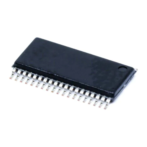
Texas Instruments ADS868 Series Manual

Texas Instruments ADS868 Series Manual

16-bit, 500-ksps, 4- and 8-channel, single-supply, sar adcs with bipolar input ranges
Table of Contents

Advertisement

Quick Links

ADS868x 16-Bit, 500-kSPS, 4- and 8-Channel, Single-Supply, SAR ADCs with

1 Features

16-Bit ADCs with Integrated Analog Front-End
1
4-, 8-Channel MUX with Auto and Manual Scan
Channel-Independent Programmable Input
Ranges:
– Bipolar: ±10.24 V, ±5.12 V, ±2.56 V
– Unipolar: 10.24 V, 5.12 V
5-V Analog Supply: 1.65-V to 5-V I/O Supply
Constant Resistive Input Impedance: 1 MΩ
Input Overvoltage Protection: Up to ±20 V
On-Chip, 4.096-V Reference with Low Drift
Excellent Performance:
– 500-kSPS Aggregate Throughput
– DNL: ±0.5 LSB; INL: ±0.75 LSB
– Low Drift for Gain Error and Offset
– SNR: 92 dB; THD: –102 dB
– Low Power: 65 mW
AUX Input → Direct Connection to ADC Inputs
SPI™-Compatible Interface with Daisy-Chain
Industrial Temperature Range: –40°C to 125°C
TSSOP-38 Package (9.7 mm × 4.4 mm)
Simplified Block Diagram
AVDD
1 M:
AIN_0P
OVP
2nd-Order
PGA
AIN_0GND
LPF
OVP
1 M:
V
B0
1 M:
AIN_1P
OVP
2nd-Order
PGA
AIN_1GND
LPF
OVP
1 M:
V
B1
1 M:
AIN_2P
OVP
2nd-Order
PGA
AIN_2GND
LPF
OVP
1 M:
V
B2
1 M:
AIN_3P
OVP
2nd-Order
PGA
AIN_3GND
LPF
OVP
1 M:
V
B3
1 M:
AIN_4P
OVP
2nd-Order
PGA
AIN_4GND
LPF
OVP
1 M:
V
B4
1 M:
AIN_5P
OVP
2nd-Order
PGA
AIN_5GND
LPF
OVP
1 M:
V
B5
1 M:
AIN_6P
OVP
2nd-Order
PGA
AIN_6GND
LPF
OVP
1 M:
V
B6
1 M:
AIN_7P
OVP
2nd-Order
PGA
AIN_7GND
LPF
OVP
1 M:
V
B7
AUX_IN
AUX_GND
AGND
1
An IMPORTANT NOTICE at the end of this data sheet addresses availability, warranty, changes, use in safety-critical applications,
intellectual property matters and other important disclaimers. PRODUCTION DATA.
Sample &
Product
Buy
Folder
Bipolar Input Ranges
DVDD
ADS8688
ADC
ADS8684
Driver
ADC
Driver
Digital
ADC
Logic
Driver
&
CS
Interface
SCLK
ADC
Driver
SDI
SDO
16-bit
ADC
Driver
SAR ADC
DAISY
REFSEL
ADC
Oscillator
Driver
RST / PD
ADC
Driver
REFCAP
REFIO
ADC
Driver
4.096V
Reference
DGND
REFGND
Tools &
Technical
Software
Documents

2 Applications

Power Automation
Protection Relays
PLC Analog Input Modules

3 Description

The ADS8684 and ADS8688 are 4- and 8-channel,
integrated data acquisition systems based on a 16-bit
successive approximation (SAR) analog-to-digital
converter (ADC), operating at a throughput of
500-kSPS. The devices feature integrated analog
front-end circuitry for each input channel with
overvoltage protection up to ±20 V, a 4- or 8-channel
multiplexer with automatic and manual scanning
modes, and an on-chip, 4.096-V reference with low
temperature drift. Operating on a single 5-V analog
supply, each input channel on the devices can
support true bipolar input ranges of ±10.24 V,
±5.12 V, and ±2.56 V, as well as unipolar input
ranges of 0 V to 10.24 V and 0 V to 5.12 V. The gain
of the analog front-end for all input ranges is
accurately trimmed to ensure a high dc precision. The
input range selection is software-programmable and
independent for each channel. The devices offer a
1-MΩ constant resistive input impedance irrespective
of the selected input range.
The ADS8684 and ADS8688 offer a simple SPI-
compatible serial interface to the digital host and also
support daisy-chaining of multiple devices. The digital
supply operates from 1.65 V to 5.25 V, enabling
direct interface to a wide range of host controllers.
Device Information
PART NUMBER
ADS868x
(1) For all available packages, see the orderable addendum at
the end of the datasheet.
Gain Error versus Temperature
0.05
0.03
0.01
-0.01
-0.03
-0.05
±40
±7
Support &
Reference
Community
Design
ADS8684, ADS8688
SBAS582C – JULY 2014 – REVISED APRIL 2015
(1)
PACKAGE
BODY SIZE (NOM)
TSSOP (38)
9.70 mm × 4.40 mm
-----
± 2.5*V
-----
± 1.25*V
----- ± 0.625*V
------ +2.5*V
REF
------+1.25*V
26
59
92
o
Free-Air Temperature (
C)
REF
REF
REF
REF
125
C026

Advertisement

Table of Contents
loading
Need help?

Need help?

Do you have a question about the ADS868 Series and is the answer not in the manual?

Questions and answers

Summary of Contents for Texas Instruments ADS868 Series

  • Page 1: Features

    Sample & Support & Reference Product Tools & Technical Community Design Folder Software Documents ADS8684, ADS8688 SBAS582C – JULY 2014 – REVISED APRIL 2015 ADS868x 16-Bit, 500-kSPS, 4- and 8-Channel, Single-Supply, SAR ADCs with Bipolar Input Ranges 1 Features 2 Applications •...
  • Page 2: Table Of Contents

    Changed Program Register Description section ......................... Changes from Revision A (July 2014) to Revision B Page • Made changes to product preview data sheet, released to Production Data................. Submit Documentation Feedback Copyright © 2014–2015, Texas Instruments Incorporated Product Folder Links: ADS8684 ADS8688...
  • Page 3 SBAS582C – JULY 2014 – REVISED APRIL 2015 Changes from Original (July 2014) to Revision A Page • Made changes to product preview data sheet........................Submit Documentation Feedback Copyright © 2014–2015, Texas Instruments Incorporated Product Folder Links: ADS8684 ADS8688...
  • Page 4: Deleted Footnote From Device Comparison Table

    Analog input Auxiliary input channel: positive input. Decouple with AUX_GND on pin 11. AUX_GND Analog input Auxiliary input channel: negative input. Decouple with AUX_IN on pin 10. Submit Documentation Feedback Copyright © 2014–2015, Texas Instruments Incorporated Product Folder Links: ADS8684 ADS8688...
  • Page 5 Do not connect this pin to any node; must remain floating. Digital output Data output for serial communication SCLK Digital input Clock input for serial communication Digital input Active low logic input; chip-select signal Submit Documentation Feedback Copyright © 2014–2015, Texas Instruments Incorporated Product Folder Links: ADS8684 ADS8688...
  • Page 6: Esd Ratings

    Junction-to-board characterization parameter 29.8 Junction-to-case (bottom) thermal resistance θJC(bot) (1) For more information about traditional and new thermal metrics, see the IC Package Thermal Metrics application report, SPRA953. Submit Documentation Feedback Copyright © 2014–2015, Texas Instruments Incorporated Product Folder Links: ADS8684 ADS8688...
  • Page 7: Electrical Characteristics

    (C) Typical value only for information, provided by design simulation. (2) Ideal input span, does not include gain or offset error. Submit Documentation Feedback Copyright © 2014–2015, Texas Instruments Incorporated Product Folder Links: ADS8684 ADS8688...
  • Page 8 Maximum throughput rate kSPS without latency (3) LSB = least significant bit. (4) This parameter is the endpoint INL, not best fit INL. (5) FSR = full-scale range. Submit Documentation Feedback Copyright © 2014–2015, Texas Instruments Incorporated Product Folder Links: ADS8684 ADS8688...
  • Page 9: Changed Auxiliary Channel, Sinad And Sfdr Typical Specifications In Electrical Characteristics Table

    (8) Memory crosstalk is measured by applying a full-scale sinusoidal signal up to 10 kHz to a channel, which is selected in the multiplexing sequence, and measuring its effect on the output of the next selected channel, for all combinations of input channels. Submit Documentation Feedback Copyright © 2014–2015, Texas Instruments Incorporated Product Folder Links: ADS8684 ADS8688...
  • Page 10 Only for SDO µA Internal pin capacitance TEMPERATURE RANGE Operating free-air temperature –40 °C (9) Does not include the variation in voltage resulting from solder shift effects. Submit Documentation Feedback Copyright © 2014–2015, Texas Instruments Incorporated Product Folder Links: ADS8684 ADS8688...
  • Page 11: Timing Requirements: Serial Interface

    PH_CS SCLK D_CKCS SU_CSCK PH_CK PL_CK SCLK HT_CKDO DZ_CSDO DZ_CSDO SU_DOCK Data from sample N SU_DICK HT_CKDI SU_DSYCK HT_CKDSY DAISY Figure 1. Serial Interface Timing Diagram Submit Documentation Feedback Copyright © 2014–2015, Texas Instruments Incorporated Product Folder Links: ADS8684 ADS8688...
  • Page 12: Typical Characteristics

    = ±2.5 × V range = ±1.25 × V Figure 6. DC Histogram for Mid-Scale Inputs (±2.5 × V Figure 7. DC Histogram for Mid-Scale Inputs (±1.25 × V Submit Documentation Feedback Copyright © 2014–2015, Texas Instruments Incorporated Product Folder Links: ADS8684 ADS8688...
  • Page 13 Free-Air Temperature ( Codes (LSB) C014 C013 All input ranges Range = ±2.5 × V Figure 12. DNL vs Temperature Figure 13. Typical INL for All Codes Submit Documentation Feedback Copyright © 2014–2015, Texas Instruments Incorporated Product Folder Links: ADS8684 ADS8688...
  • Page 14 Range = ±2.5 × V Range = ±1.25 × V Figure 18. INL vs Temperature (±2.5 × V Figure 19. INL vs Temperature (±1.25 × V Submit Documentation Feedback Copyright © 2014–2015, Texas Instruments Incorporated Product Folder Links: ADS8684 ADS8688...
  • Page 15 C025 Range = ±2.5 × V Range = ±2.5 × V Figure 24. Typical Histogram for Offset Drift Figure 25. Offset Error vs Temperature Across Channels Submit Documentation Feedback Copyright © 2014–2015, Texas Instruments Incorporated Product Folder Links: ADS8684 ADS8688...
  • Page 16 SINAD = 91.2 dB, THD = 105 dB, SFDR = 107 dB Figure 30. Typical FFT Plot (±2.5 × V Figure 31. Typical FFT Plot (±1.25 × V Submit Documentation Feedback Copyright © 2014–2015, Texas Instruments Incorporated Product Folder Links: ADS8684 ADS8688...
  • Page 17 1000 10000 ±40 ±7 Free-Air Temperature ( Input Frequency (Hz) C036 C037 = 1 kHz Figure 36. SNR vs Temperature Figure 37. SINAD vs Input Frequency Submit Documentation Feedback Copyright © 2014–2015, Texas Instruments Incorporated Product Folder Links: ADS8684 ADS8688...
  • Page 18 Input Frequency (Hz) C042 C043 Input = 2 × maximum input voltage Figure 42. Isolation Crosstalk vs Frequency Figure 43. Memory Crosstalk vs Frequency for Overrange Inputs Submit Documentation Feedback Copyright © 2014–2015, Texas Instruments Incorporated Product Folder Links: ADS8684 ADS8688...
  • Page 19 ±7 Free-Air Temperature ( Free-Air Temperature ( C063 Figure 48. AVDD Current vs Temperature for the ADS8684 Figure 49. AVDD Current vs Temperature (During Sampling) (STANDBY) Submit Documentation Feedback Copyright © 2014–2015, Texas Instruments Incorporated Product Folder Links: ADS8684 ADS8688...
  • Page 20 = 4.096 V, and f = 500 kSPS, unless otherwise noted. SAMPLE ±40 ±7 Free-Air Temperature ( C060 Figure 50. AVDD Current vs Temperature (Power Down) Submit Documentation Feedback Copyright © 2014–2015, Texas Instruments Incorporated Product Folder Links: ADS8684 ADS8688...
  • Page 21: Detailed Description

    1 M: 1 M: AIN_6P 2nd-Order AIN_6GND REFCAP Driver 1 M: REFIO 1 M: AIN_7P 2nd-Order AIN_7GND Driver 4.096V 1 M: Reference AUX_IN AUX_GND AGND DGND REFGND Submit Documentation Feedback Copyright © 2014–2015, Texas Instruments Incorporated Product Folder Links: ADS8684 ADS8688...
  • Page 22: Feature Description

    In order to maintain the dc accuracy of the system, matching the external source impedance on the AIN_nP input pin with an equivalent resistance on the AIN_nGND pin is recommended. This matching helps to cancel any additional offset error contributed by the external resistance. Submit Documentation Feedback Copyright © 2014–2015, Texas Instruments Incorporated Product Folder Links: ADS8684 ADS8688...
  • Page 23 OVP voltage range. Note that higher source impedance results in gain errors and contributes to overall system noise performance. Submit Documentation Feedback Copyright © 2014–2015, Texas Instruments Incorporated Product Folder Links: ADS8684 ADS8688...
  • Page 24 C004 Figure 53. I-V Curve for an Input OVP Circuit Figure 54. I-V Curve for an Input OVP Circuit (AVDD = 5 V) (AVDD = Floating) Submit Documentation Feedback Copyright © 2014–2015, Texas Instruments Incorporated Product Folder Links: ADS8684 ADS8688...
  • Page 25: Changed Range_Chn[2:0] To Range_Chn[3:0] In Programmable Gain Amplifier (Pga) Section

    16-bit accuracy within the acquisition time of the ADC, irrespective of the input levels on the respective channels. Submit Documentation Feedback Copyright © 2014–2015, Texas Instruments Incorporated Product Folder Links: ADS8684 ADS8688...
  • Page 26 (such as the OPA320). AVDD 4.096 REFSEL REFIO 102F REFCAP 222F REFGND AGND Figure 57. Device Connections for Using an Internal 4.096-V Reference Submit Documentation Feedback Copyright © 2014–2015, Texas Instruments Incorporated Product Folder Links: ADS8684 ADS8688...
  • Page 27 ADS8684 and ADS8688 in the second pass to minimize device exposure to thermal stress. Error in REFIO Voltage (mV) C065 Figure 59. Solder Heat Shift Distribution Histogram Submit Documentation Feedback Copyright © 2014–2015, Texas Instruments Incorporated Product Folder Links: ADS8684 ADS8688...
  • Page 28 AVDD REF5040 (Refer to Device Datasheet for REFIO Detailed Pin Configuration) REFCAP 22 2F REFGND AGND Figure 62. Device Connections for Using an External 4.096-V Reference Submit Documentation Feedback Copyright © 2014–2015, Texas Instruments Incorporated Product Folder Links: ADS8684 ADS8688...
  • Page 29 The AUX channel in the ADS8684 and ADS8688 offers a true 16-bit performance with no missing codes. Some typical performance characteristics of the AUX channel are illustrated in Figure 65 Figure Submit Documentation Feedback Copyright © 2014–2015, Texas Instruments Incorporated Product Folder Links: ADS8684 ADS8688...
  • Page 30 Distortion. In order to achieve the distortion performance of the AUX channel, the distortion of the input driver must be at least 10 dB lower than the specified distortion of the internal ADC, as shown in Equation Submit Documentation Feedback Copyright © 2014–2015, Texas Instruments Incorporated Product Folder Links: ADS8684 ADS8688...
  • Page 31 2.56 V –2.56 V 5.12 V 78.125 0 to 2.5 × V 10.24 V 10.24 V 156.25 0 to 1.25 × V 5.12 V 5.12 V 78.125 Submit Documentation Feedback Copyright © 2014–2015, Texas Instruments Incorporated Product Folder Links: ADS8684 ADS8688...
  • Page 32: Device Functional Modes

    The SDO line goes low after the entire data frame is output and goes to a Hi-Z state when CS goes high. Submit Documentation Feedback Copyright © 2014–2015, Texas Instruments Incorporated Product Folder Links: ADS8684 ADS8688...
  • Page 33 When the RST/PD pin is pulled back to a logic high level, the devices wake-up in a default state in which the program registers are reset to their default values. Submit Documentation Feedback Copyright © 2014–2015, Texas Instruments Incorporated Product Folder Links: ADS8684 ADS8688...
  • Page 34: Changed Sdo To Sdi In Second Sentence Of Event 3 In Data Acquisition Example Section

    70. However, there are applications that require multiple ADCs but the host controller has limited interfacing capability. This section describes two connection topologies that can be used to address the requirements of such applications. Submit Documentation Feedback Copyright © 2014–2015, Texas Instruments Incorporated Product Folder Links: ADS8684 ADS8688...
  • Page 35 64 SCLK cycles for the entire data frame. Note that the overall throughput of the system is proportionally reduced with the number of devices connected in a daisy-chain configuration. Submit Documentation Feedback Copyright © 2014–2015, Texas Instruments Incorporated Product Folder Links: ADS8684 ADS8688...
  • Page 36 (SDO and SCLK). This loading may lead to digital timing errors. This limitation can be overcome by using digital buffers on the shared outputs from the host controller before being fed into additional devices. Submit Documentation Feedback Copyright © 2014–2015, Texas Instruments Incorporated Product Folder Links: ADS8684 ADS8688...
  • Page 37: Changed Continued Operation In The Selected Mode Section

    (PROG mode), then the device retains the current settings of the program registers. The device goes back to IDLE mode and waits for the user to enter a proper command to execute the program register read or write configuration. Submit Documentation Feedback Copyright © 2014–2015, Texas Instruments Incorporated Product Folder Links: ADS8684 ADS8688...
  • Page 38: Changed Frame Abort Condition Section

    SDI is LOW in a data frame STDBY COMMAND ± 8200h Data from sample N Figure 77. Enter and Remain in STDBY Mode Timing Diagram Submit Documentation Feedback Copyright © 2014–2015, Texas Instruments Incorporated Product Folder Links: ADS8684 ADS8688...
  • Page 39 STDBY Mode on CS Rising Edge Min width of CS HIGH = 20µs for valid sample SCLK AUTO_RST Command MAN_CH_n Command Figure 78. Exit STDBY Mode Timing Diagram Submit Documentation Feedback Copyright © 2014–2015, Texas Instruments Incorporated Product Folder Links: ADS8684 ADS8688...
  • Page 40: Changed Second Paragraph Of Power-Down Mode Section: Added Clarification To Description Of Pwr_Dn Mode

    Device exits PWR_DN Mode, but frame after recovery from waits 15ms for 16-bit settling PWR_DN mode SCLK AUTO_RST Command MAN_CH_n Command Invalid Data Figure 80. Exit PWR_DN Mode Timing Diagram Submit Documentation Feedback Copyright © 2014–2015, Texas Instruments Incorporated Product Folder Links: ADS8684 ADS8688...
  • Page 41: Changed First Two Paragraphs Of Auto Channel Enable With Reset Section

    Mode Setting AUTO_RST Mode AUTO_RST Mode (Channel sequence re-started from (Channels 0-3 are selected in sequence) lowest count) Figure 82. Device Operation Example in AUTO_RST Mode Submit Documentation Feedback Copyright © 2014–2015, Texas Instruments Incorporated Product Folder Links: ADS8684 ADS8688...
  • Page 42: Changed First Paragraph Of Manual Channel N Select Section

    (Ch 1 is selected and device continuously converts Ch 1 if NO_OP command is provided) (Transition from Ch1 to Ch 3) Figure 84. Device Operation in MAN_Ch_n Mode Submit Documentation Feedback Copyright © 2014–2015, Texas Instruments Incorporated Product Folder Links: ADS8684 ADS8688...
  • Page 43 Based on Previous Mode Setting MAN_Ch_n Mode AUTO_RST Mode Figure 86. Transitioning from MAN_Ch_n to AUTO_RST Mode (Channels 0 and 5 are Selected for Auto Sequence) Submit Documentation Feedback Copyright © 2014–2015, Texas Instruments Incorporated Product Folder Links: ADS8684 ADS8688...
  • Page 44: Changed Second Paragraph Of Reset Program Registers Section: Added Clarity To Description Of Rst Mode

    CS rising edge command or after reading frame data SCLK Reset Program Registers (RST) ± 8500h Data from sample N Figure 87. Reset Program Registers (RST) Timing Diagram Submit Documentation Feedback Copyright © 2014–2015, Texas Instruments Incorporated Product Folder Links: ADS8684 ADS8688...
  • Page 45: Register Maps

    Submit Documentation Feedback Copyright © 2014–2015, Texas Instruments Incorporated Product Folder Links: ADS8684 ADS8688...
  • Page 46 (Bits 7-0) ADDR[6:0] XXXXX 0000 000 DOUT[7:0] SCLK ADDR [6:0] X X X X X X DOUT [7:0] Figure 89. Program Register Read Cycle Timing Diagram Submit Documentation Feedback Copyright © 2014–2015, Texas Instruments Incorporated Product Folder Links: ADS8684 ADS8688...
  • Page 47 (2) Shading indicates bits or registers that are not included in the 4-channel version of the device. A write operation on any of these bits or registers has no effect on device behavior. A read operation on any of these bits or registers outputs all 1's on the SDO line. Submit Documentation Feedback Copyright © 2014–2015, Texas Instruments Incorporated Product Folder Links: ADS8684 ADS8688...
  • Page 48 Channel 0 enable. CH0_EN 0 = Channel 0 is not selected for sequencing in AUTO_RST mode 1 = Channel 0 is selected for sequencing in AUTO_RST mode Submit Documentation Feedback Copyright © 2014–2015, Texas Instruments Incorporated Product Folder Links: ADS8684 ADS8688...
  • Page 49 AUTO_RST sequence 1 = The analog front end on channel 0 is powered down and channel 0 cannot be included in the AUTO_RST sequence Submit Documentation Feedback Copyright © 2014–2015, Texas Instruments Incorporated Product Folder Links: ADS8684 ADS8688...
  • Page 50 0111 = Channel 7 (valid only for the ADS8688) Two bits of device address (mainly useful in daisy-chain mode). Three LSB bits of input voltage range (refer to the Range Select Registers section). Submit Documentation Feedback Copyright © 2014–2015, Texas Instruments Incorporated Product Folder Links: ADS8684 ADS8688...
  • Page 51 LEGEND: R = Read only; -n = value after reset Table 16. Command Read-Back Register Field Descriptions Field Type Reset Description COMMAND_WORD[15:8] Command executed in previous data frame. Submit Documentation Feedback Copyright © 2014–2015, Texas Instruments Incorporated Product Folder Links: ADS8684 ADS8688...
  • Page 52: Application And Implementation

    The key electrical parameters include amplitude, frequency, and phase, which are important for calculating the power factor, power quality, and other parameters of the power system. Submit Documentation Feedback Copyright © 2014–2015, Texas Instruments Incorporated Product Folder Links: ADS8684 ADS8688...
  • Page 53: Typical Applications

    (2) Measured phase value (before compensation) includes phase difference between any two channels resulting from multiplexing ADC inputs. (3) The algorithm subtracts theoretical phase difference from the measured phase to compensate for the phase difference resulting from the MUX inputs. Submit Documentation Feedback Copyright © 2014–2015, Texas Instruments Incorporated Product Folder Links: ADS8684 ADS8688...
  • Page 54 Protection 0 ± 20 mA 3.3 VDC 4 ± 20 mA Filter Digital Isolator ISO7141CC EEPROM Figure 97. 16-Bit, 8-Channel, Integrated Analog Input Module for PLCs Submit Documentation Feedback Copyright © 2014–2015, Texas Instruments Incorporated Product Folder Links: ADS8684 ADS8688...
  • Page 55 The protection circuitry makes use of the transient voltage suppressor (TVS) and ESD diodes. The RC low-pass mode filters are used on each analog input before the input reaches the ADS8688, which eliminates any high-frequency noise pickups and minimizes aliasing. Submit Documentation Feedback Copyright © 2014–2015, Texas Instruments Incorporated Product Folder Links: ADS8684 ADS8688...
  • Page 56 For a step-by-step design procedure, circuit schematics, bill of materials, PCB files, simulation results, and test results, refer to 16-Bit, 8-Channel, Integrated Analog Input Module for Programmable Logic Controllers (PLCs) (TIDU365). Submit Documentation Feedback Copyright © 2014–2015, Texas Instruments Incorporated Product Folder Links: ADS8684 ADS8688...
  • Page 57: Layout Guidelines

    COG (NPO) ceramic capacitors provide the best capacitance precision. The type of dielectric used in COG (NPO) ceramic capacitors provides the most stable electrical properties over voltage, frequency, and temperature changes. Submit Documentation Feedback Copyright © 2014–2015, Texas Instruments Incorporated Product Folder Links: ADS8684 ADS8688...
  • Page 58: Layout Example

    16: AIN_0P 23: AIN_3P 17: AIN_0GND 22: AIN_3GND 18: AIN_1P 21: AIN_2P 19: AIN_1GND 20: AIN_2GND Analog Pins Figure 101. Board Layout for the ADS8684 and ADS8688 Submit Documentation Feedback Copyright © 2014–2015, Texas Instruments Incorporated Product Folder Links: ADS8684 ADS8688...
  • Page 59: Device And Documentation Support

    All other trademarks are the property of their respective owners. 12.4 Electrostatic Discharge Caution This integrated circuit can be damaged by ESD. Texas Instruments recommends that all integrated circuits be handled with appropriate precautions. Failure to observe proper handling and installation procedures can cause damage.
  • Page 60 PACKAGE OPTION ADDENDUM www.ti.com 6-Feb-2020 PACKAGING INFORMATION Orderable Device Status Package Type Package Pins Package Eco Plan Lead/Ball Finish MSL Peak Temp Op Temp (°C) Device Marking Samples Drawing (4/5) ADS8684IDBT ACTIVE TSSOP Green (RoHS NIPDAU Level-2-260C-1 YEAR -40 to 125 ADS8684 &...
  • Page 61 PACKAGE OPTION ADDENDUM www.ti.com 6-Feb-2020 continues to take reasonable steps to provide representative and accurate information but may not have conducted destructive testing or chemical analysis on incoming materials and chemicals. TI and TI suppliers consider certain information to be proprietary, and thus CAS numbers and other limited information may not be available for release. In no event shall TI's liability arising out of such information exceed the total purchase price of the TI part(s) at issue in this document sold by TI to Customer on an annual basis.
  • Page 62 PACKAGE MATERIALS INFORMATION www.ti.com 20-Mar-2015 TAPE AND REEL INFORMATION *All dimensions are nominal Device Package Package Pins Reel Reel Pin1 Type Drawing Diameter Width (mm) (mm) (mm) (mm) (mm) Quadrant (mm) W1 (mm) ADS8684IDBTR TSSOP 2000 330.0 16.4 10.2 12.0 16.0 ADS8688IDBTR TSSOP...
  • Page 63 PACKAGE MATERIALS INFORMATION www.ti.com 20-Mar-2015 *All dimensions are nominal Device Package Type Package Drawing Pins Length (mm) Width (mm) Height (mm) ADS8684IDBTR TSSOP 2000 367.0 367.0 38.0 ADS8688IDBTR TSSOP 2000 367.0 367.0 38.0 Pack Materials-Page 2...
  • Page 64 PACKAGE OUTLINE DBT0038A TSSOP - 1.2 mm max height SCALE 2.000 SMALL OUTLINE PACKAGE SEATING 6.55 6.25 TYP PLANE 0.1 C PIN 1 INDEX AREA 38 X 0.5 9.75 9.65 NOTE 3 38 X 0.23 0.17 4.45 1.2 MAX C A B 4.35 NOTE 4 0.25...
  • Page 65 EXAMPLE BOARD LAYOUT DBT0038A TSSOP - 1.2 mm max height SMALL OUTLINE PACKAGE 38 X (1.5) SYMM (R0.05) TYP 38 X (0.3) 38 X (0.5) SYMM (5.8) LAND PATTERN EXAMPLE EXPOSED METAL SHOWN SCALE: 10X SOLDER MASK METAL UNDER SOLDER MASK METAL OPENING SOLDER MASK...
  • Page 66 EXAMPLE STENCIL DESIGN DBT0038A TSSOP - 1.2 mm max height SMALL OUTLINE PACKAGE 38 X (1.5) SYMM (R0.05) TYP 38 X (0.3) 38 X (0.5) SYMM (5.8) SOLDER PASTE EXAMPLE BASED ON 0.125 mm THICK STENCIL SCALE: 10X 4220221/A 05/2020 NOTES: (continued) 8.
  • Page 67 TI products. TI’s provision of these resources does not expand or otherwise alter TI’s applicable warranties or warranty disclaimers for TI products. Mailing Address: Texas Instruments, Post Office Box 655303, Dallas, Texas 75265 Copyright © 2020, Texas Instruments Incorporated...

This manual is also suitable for:

Ads8684Ads8688Ads8688idbtrAds8684idbtr

Table of Contents