Table of Contents
Advertisement
Quick Links
Advertisement
Table of Contents

Subscribe to Our Youtube Channel
Related Manuals for Seiko SLP721RT Series


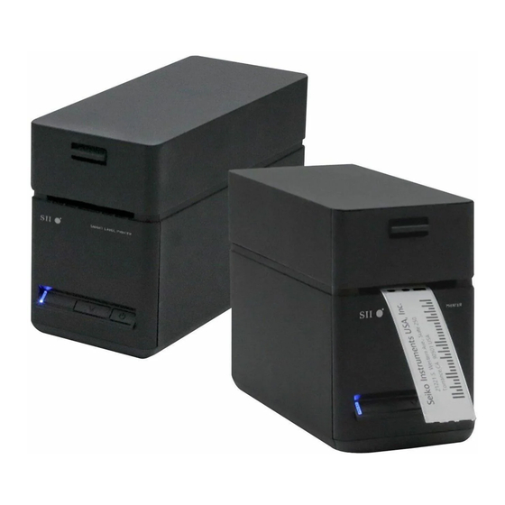
Summary of Contents for Seiko SLP721RT Series
- Page 1 SLP721RT SERIES THERMAL PRINTER SERVICE MANUAL Rev.01...
- Page 2 All other trademarks are the properties of their respective companies. Seiko Instruments Inc. (hereinafter referred to as "SII") has prepared this manual for use by SII personnel, licensees, and customers. The information contained herein is the property of SII and shall not be reproduced in whole or in part without the prior written approval of SII.
- Page 3 PREFACE This service manual describes the information necessary to perform the maintenance service for the SLP721RT series thermal printer (hereinafter referred to as "printer"). For a better understanding, the following documents are necessary to read together with this manual. SLP721RT SERIES Thermal Printer USER'S GUIDE •...
-
Page 4: Table Of Contents
TABLE OF CONTENTS CHAPTER 1 DISASSEMBLY/REASSEMBLY (PARTS CATALOG) CHAPTER 2 CIRCUIT DIAGRAM CHAPTER 3 TROUBLESHOOTING FAILURE DIAGNOSTICS ..................3-1 CHAPTER 4 TEST PRINT TEST PRINT ......................4-1 SPECIAL TEST PRINT ..................... 4-3 CHAPTER 5 PACKING SPECIFICATIONS PACKING MATERIAL ....................5-1 DIMENSIONS AND MASS .................. - Page 5 FIGURES Figure 1-1 Illustrated Parts Breakdown (Printer Whole Body) ........... 1-2 Figure 1-2 Illustrated Parts Breakdown (BOTTOM COVER UNIT Installation) ......1-4 Figure 1-3 Illustrated Parts Breakdown (SLP721RT MAIN PCB BLOCK Installation) ............1-5 Figure 1-4 Illustrated Parts Breakdown (FRONT COVER UNIT Installation) ......1-8 Figure 1-5 Illustrated Parts Breakdown (FRONT COVER UNIT Reassembly) ......
- Page 6 Figure 2-17 Circuit Diagram of Main Board for Wireless LAN Model (Japan Only) (SLP721RT-W MAIN PCB BLOCK A) (1/8) ............2-18 Figure 2-18 Circuit Diagram of Main Board for Wireless LAN Model (Japan Only) (SLP721RT-W MAIN PCB BLOCK A) (2/8) ............2-19 Figure 2-19 Circuit Diagram of Main Board for Wireless LAN Model (Japan Only) (SLP721RT-W MAIN PCB BLOCK A) (3/8) ............
-
Page 7: Disassembly/Reassembly (Parts Catalog)
CHAPTER 1 DISASSEMBLY/REASSEMBLY (PARTS CATALOG) Illustrated parts breakdown and the parts list of the unit are shown below. The numbers of the illustrated parts breakdown and those in the parts list correspond with each other. Refer to the illustrated parts breakdown for disassembly and reassembly. ・Be careful to sharp edges during disassembly/reassembly. - Page 8 Figure 1-1 Illustrated Parts Breakdown (Printer Whole Body)
- Page 9 When pasting 50, make sure that the orientation is correct as shown in the figure below.
- Page 10 Figure 1-2 Illustrated Parts Breakdown (BOTTOM COVER UNIT Installation) ・Screw 1 to 11 with 47. Tighten screw 47 with tightening torque 63.7 cN·m (6.50 kgf·cm). ・Paste 44 on 1. When replacing the BOTTOM COVER UNIT: Depending on the interface type of the SLP721RT-* MAIN PCB BLOCK A to be installed, cut and remove the tabs shown in the figure below.
- Page 11 Figure 1-3 Illustrated Parts Breakdown (SLP721RT-* MAIN PCB BLOCK A Installation)
- Page 12 ・Solder 23, 24, and 32. ・Insert the FFC of 7 into CN8 on 25, 9 into CN11 on 25, 14 into CN10 on 25, and 11 into CN9 on 25. ・Install the FFC of 34 and 35 into CN5 and CN6 on 25. ・Screw 11, 24, and 25 with 47.
- Page 13 When inserting the FPC on the SLP721RT-* MAIN PCB BLOCK A (CN10), insert it to the connector in the correct orientation, paying attention to the front and back as shown in the figure below. Incorrect Correct (The front and back of the connection terminals are wrong.) Pass the tips of terminal of the FG CABLE A installed on the TOP COVER UNIT and FG CABLE B installed on the PAPER HOLDER UNIT through the hole as shown in the figure below and solder them..
- Page 14 Figure 1-4 Illustrated Parts Breakdown (FRONT COVER UNIT Installation) ・Screw 3, 5, and 11 with 47. Tighten screw 47 with tightening torque 63.7 cN·m (6.50 kgf·cm).
- Page 15 * Exclusive part for white model Figure 1-5 Illustrated Parts Breakdown (FRONT COVER UNIT Reassembly) ・For white model, install 51 on 9. ・Install 6, 7, 8, 9, and 10 on 5. ・Screw 7 to 8 with 46. Tighten screw 46 with tightening torque 23.7 cN·m (2.42 kgf·cm). When assembling 51 and 9, install them so that 51 is inserted deeply in the correct orientation as shown in the figure below.
- Page 16 Correct Incorrect Incorrect (Wrong orientation) (Inside out) Correct Insertion Insufficient Insertion When replacing the TAKEN SENSOR PCB ASSY, fix it with the 2 hooks aligned on the FRONT COVER as shown in the figure below. Hooks 1-10...
- Page 17 Install the TAKEN SENSOR PCB ASSY so that the lead wires pass through the 3 guides as shown in the figure below. Guide Guide 1-11...
- Page 18 Figure 1-6 Illustrated Parts Breakdown (SIDE COVER Installation) 1-12...
- Page 19 Fastening surface ・Install 3 on 11. Install the fastening surface of 3 to 11 through the path indicated by the arrow in the figure. ・Screw 3 to 11 with 47. Tighten screw 47 with tightening torque 63.7 cN·m (6.50 kgf·cm). 1-13...
- Page 20 Figure 1-7 Illustrated Parts Breakdown (TOP COVER UNIT Installation) ・Install the boss of 27 in the hole of 11. ・Pass the FFC of 34 and 35 through the hooks of 11. ・Pass 32 through the guide of 11. 1-14...
- Page 21 When installing the TOP COVER UNIT, install it so that the TOP COVER SPRING is held by the embossed portion of the PAPER HOLDER. When installing or removing the TOP COVER UNIT, the TOP COVER SPRING should be hold so that it does not project out or fall off.
- Page 22 Figure 1-8 Illustrated Parts Breakdown (TOP COVER UNIT Reassembly) ・After installing 29 on 28, install it on 27. ・Screw MECH BLOCK to 26 with 45. Tighten screw 45 with tightening torque 59.0 cN·m (6.02 kgf·cm). ・Install 41 and 42 on 27. ・Screw 27 to 26 with 48.
- Page 23 When assembling MECH BLOCK and TOP COVER BASE, install them so that LOCK ARM SHAFT is held by the 2 hooks as shown in the figure below. LOCK ARM SHAFT Hook Hook When removing the COVER DAMPER UNIT, place it in the position shown in the figure below and pull it out in the direction of the arrow in the figure.
- Page 24 When installing or removing the TOP COVER BASE, the TOP COVER SPRING should be hold so that it does not project out or fall off. Tabs When assembling the MECH BLOCK, bend the FFC in 2 places as shown in the figure below and pass the hooks through them, and install the lead wires so that they pass through the guides.
- Page 25 Figure 1-9 Illustrated Parts Breakdown (MECH BLOCK Reassembly) ・Screw 35 to 31 with 45. Tighten screw 45 with tightening torque 59.0 cN·m (6.02 kgf·cm). ・Install 40 on 31 and 36. ・Install 39 on 38, and then install 38 on 31 and 36. When replacing the thermal head, assemble the FFC in the correct orientation as shown in the figure below, paying attention to the front and back of the FFC.
- Page 26 When installing MECH BLOCK, pass the FG CABLE A through the hook as shown in the figure below. Hook 1-20...
- Page 27 Figure 1-10 Illustrated Parts Breakdown (PAPER HOLDER UNIT Reassembly) ・After installing 21 on 20, install it on 11. ・Screw 22 to 11 with 45 and 49. Tighten screws 45 and 49 with tightening torque 59.0 cN·m (6.02 kgf·cm). ・Screw 11 to 23 with 48. Tighten screw 48 with tightening torque 63.7 cN·m (6.50 kgf·cm).
- Page 28 When assembling the PAPER HOLDER UNIT, pass the FG CABLE B through the hook as shown in the figure below. Hook 1-22...
-
Page 29: Table 1-2 Parts List
Table 1-2 Parts List Parts No. Parts Name Qty. Notes U001455928XX For Black model BOTTOM COVER UNIT U001465661XX For White model U001460891XX RUBBER FOOT U001455300XX For Black model SIDE COVER U001465547XX For White model U001455930XX For Black model FRONT COVER UNIT U001465672XX For White model U001455333XX... - Page 30 Parts No. Parts Name Qty. Notes U001456042XX FFC FOR HEAD U001455851XX MOVABLE CUTTER UNIT U001455906XX For Black model LOCK ARM BLOCK U001465705XX For White model U001455243XX For Black model OPEN LEVER U001465593XX For White model U001455254XX LOCK ARM SPRING U001465176XX HEAT SHRINK TUBE U001455265XX LOCK ARM SHAFT...
-
Page 31: Chapter 2 Circuit Diagram
CHAPTER 2 CIRCUIT DIAGRAM Figure 2-1 to Figure 2-25 show the circuit diagrams of the circuit board. Figure 2-26 to Figure 2-28 show the component layouts of the circuit board. -
Page 32: Figure 2-1 Circuit Diagram Of Main Board For Usb Model (Japan Only) (Slp721Rt-U Main Pcb Block A) (1/8)
Figure 2-1 Circuit Diagram of Main Board for USB Model (Japan Only) (SLP721RT-U MAIN PCB BLOCK A) (1/8) -
Page 33: Figure 2-2 Circuit Diagram Of Main Board For Usb Model (Japan Only) (Slp721Rt-U Main Pcb Block A) (2/8)
Figure 2-2 Circuit Diagram of Main Board for USB Model (Japan Only) (SLP721RT-U MAIN PCB BLOCK A) (2/8) -
Page 34: Figure 2-3 Circuit Diagram Of Main Board For Usb Model (Japan Only) (Slp721Rt-U Main Pcb Block A) (3/8)
Figure 2-3 Circuit Diagram of Main Board for USB Model (Japan Only) (SLP721RT-U MAIN PCB BLOCK A) (3/8) -
Page 35: Figure 2-4 Circuit Diagram Of Main Board For Usb Model (Japan Only) (Slp721Rt-U Main Pcb Block A) (4/8)
Figure 2-4 Circuit Diagram of Main Board for USB Model (Japan Only) (SLP721RT-U MAIN PCB BLOCK A) (4/8) -
Page 36: Figure 2-5 Circuit Diagram Of Main Board For Usb Model (Japan Only) (Slp721Rt-U Main Pcb Block A) (5/8)
Figure 2-5 Circuit Diagram of Main Board for USB Model (Japan Only) (SLP721RT-U MAIN PCB BLOCK A) (5/8) -
Page 37: Figure 2-6 Circuit Diagram Of Main Board For Usb Model (Japan Only) (Slp721Rt-U Main Pcb Block A) (6/8)
Figure 2-6 Circuit Diagram of Main Board for USB Model (Japan Only) (SLP721RT-U MAIN PCB BLOCK A) (6/8) -
Page 38: Figure 2-7 Circuit Diagram Of Main Board For Usb Model (Japan Only) (Slp721Rt-U Main Pcb Block A) (7/8)
Figure 2-7 Circuit Diagram of Main Board for USB Model (Japan Only) (SLP721RT-U MAIN PCB BLOCK A) (7/8) -
Page 39: Figure 2-8 Circuit Diagram Of Main Board For Usb Model (Japan Only) (Slp721Rt-U Main Pcb Block A) (8/8)
Figure 2-8 Circuit Diagram of Main Board for USB Model (Japan Only) (SLP721RT-U MAIN PCB BLOCK A) (8/8) -
Page 40: Figure 2-9 Circuit Diagram Of Main Board For Ethernet + Usb Model (Slp721Rt-E Main Pcb Block A) (1/8)
Figure 2-9 Circuit Diagram of Main Board for Ethernet + USB Model (SLP721RT-E MAIN PCB BLOCK A) (1/8) 2-10... -
Page 41: Figure 2-10 Circuit Diagram Of Main Board For Ethernet + Usb Model (Slp721Rt-E Main Pcb Block A) (2/8)
Figure 2-10 Circuit Diagram of Main Board for Ethernet + USB Model (SLP721RT-E MAIN PCB BLOCK A) (2/8) 2-11... -
Page 42: Figure 2-11 Circuit Diagram Of Main Board For Ethernet + Usb Model (Slp721Rt-E Main Pcb Block A) (3/8)
Figure 2-11 Circuit Diagram of Main Board for Ethernet + USB Model (SLP721RT-E MAIN PCB BLOCK A) (3/8) 2-12... -
Page 43: Figure 2-12 Circuit Diagram Of Main Board For Ethernet + Usb Model (Slp721Rt-E Main Pcb Block A) (4/8)
Figure 2-12 Circuit Diagram of Main Board for Ethernet + USB Model (SLP721RT-E MAIN PCB BLOCK A) (4/8) 2-13... -
Page 44: Figure 2-13 Circuit Diagram Of Main Board For Ethernet + Usb Model (Slp721Rt-E Main Pcb Block A) (5/8)
Figure 2-13 Circuit Diagram of Main Board for Ethernet + USB Model (SLP721RT-E MAIN PCB BLOCK A) (5/8) 2-14... -
Page 45: Figure 2-14 Circuit Diagram Of Main Board For Ethernet + Usb Model (Slp721Rt-E Main Pcb Block A) (6/8)
Figure 2-14 Circuit Diagram of Main Board for Ethernet + USB Model (SLP721RT-E MAIN PCB BLOCK A) (6/8) 2-15... -
Page 46: Figure 2-15 Circuit Diagram Of Main Board For Ethernet + Usb Model (Slp721Rt-E Main Pcb Block A) (7/8)
Figure 2-15 Circuit Diagram of Main Board for Ethernet + USB Model (SLP721RT-E MAIN PCB BLOCK A) (7/8) 2-16... -
Page 47: Figure 2-16 Circuit Diagram Of Main Board For Ethernet + Usb Model (Slp721Rt-E Main Pcb Block A) (8/8)
Figure 2-16 Circuit Diagram of Main Board for Ethernet + USB Model (SLP721RT-E MAIN PCB BLOCK A) (8/8) 2-17... -
Page 48: Figure 2-17 Circuit Diagram Of Main Board For Wireless Lan Model (Japan Only) (Slp721Rt-W Main Pcb Block A) (1/8)
Figure 2-17 Circuit Diagram of Main Board for Wireless LAN Model (Japan Only) (SLP721RT-W MAIN PCB BLOCK A) (1/8) 2-18... -
Page 49: Figure 2-18 Circuit Diagram Of Main Board For Wireless Lan Model (Japan Only) (Slp721Rt-W Main Pcb Block A) (2/8)
Figure 2-18 Circuit Diagram of Main Board for Wireless LAN Model (Japan Only) (SLP721RT-W MAIN PCB BLOCK A) (2/8) 2-19... -
Page 50: Figure 2-19 Circuit Diagram Of Main Board For Wireless Lan Model (Japan Only) (Slp721Rt-W Main Pcb Block A) (3/8)
Figure 2-19 Circuit Diagram of Main Board for Wireless LAN Model (Japan Only) (SLP721RT-W MAIN PCB BLOCK A) (3/8) 2-20... -
Page 51: Figure 2-20 Circuit Diagram Of Main Board For Wireless Lan Model (Japan Only) (Slp721Rt-W Main Pcb Block A) (4/8)
Figure 2-20 Circuit Diagram of Main Board for Wireless LAN Model (Japan Only) (SLP721RT-W MAIN PCB BLOCK A) (4/8) 2-21... -
Page 52: Figure 2-21 Circuit Diagram Of Main Board For Wireless Lan Model (Japan Only) (Slp721Rt-W Main Pcb Block A) (5/8)
Figure 2-21 Circuit Diagram of Main Board for Wireless LAN Model (Japan Only) (SLP721RT-W MAIN PCB BLOCK A) (5/8) 2-22... -
Page 53: Figure 2-22 Circuit Diagram Of Main Board For Wireless Lan Model (Japan Only) (Slp721Rt-W Main Pcb Block A) (6/8)
Figure 2-22 Circuit Diagram of Main Board for Wireless LAN Model (Japan Only) (SLP721RT-W MAIN PCB BLOCK A) (6/8) 2-23... -
Page 54: Figure 2-23 Circuit Diagram Of Main Board For Wireless Lan Model (Japan Only) (Slp721Rt-W Main Pcb Block A) (7/8)
Figure 2-23 Circuit Diagram of Main Board for Wireless LAN Model (Japan Only) (SLP721RT-W MAIN PCB BLOCK A) (7/8) 2-24... -
Page 55: Figure 2-24 Circuit Diagram Of Main Board For Wireless Lan Model (Japan Only) (Slp721Rt-W Main Pcb Block A) (8/8)
Figure 2-24 Circuit Diagram of Main Board for Wireless LAN Model (Japan Only) (SLP721RT-W MAIN PCB BLOCK A) (8/8) 2-25... -
Page 56: Figure 2-25 Circuit Diagram Of Operation Board (Slp721Rt Op Pcb Block A)
Figure 2-25 Circuit Diagram of Operation Board (SLP721RT OP PCB BLOCK A) 2-26... -
Page 57: Figure 2-26 Component Layout Of Circuit Board (Japan Only) (Slp721Rt-U Main Pcb Block A) (Reference)
Figure 2-26 Component Layout of Circuit Board (Japan Only) (SLP721RT-U MAIN PCB BLOCK A) (Reference) 2-27... -
Page 58: Figure 2-27 Component Layout Of Circuit Board (Slp721Rt-E Main Pcb Block A) (Reference)
Figure 2-27 Component Layout of Circuit Board (SLP721RT-E MAIN PCB BLOCK A) (Reference) 2-28... -
Page 59: Figure 2-28 Component Layout Of Circuit Board (Japan Only) (Slp721Rt-W Main Pcb Block A) (Reference)
Figure 2-28 Component Layout of Circuit Board (Japan Only) (SLP721RT-W MAIN PCB BLOCK A) (Reference) 2-29... -
Page 60: Chapter 3 Troubleshooting
CHAPTER 3 TROUBLESHOOTING The printer troubles are classified into 2 types: setting problems or printer failures. This chapter describes troubleshooting in the case of printer failures. If the printer does not operate smoothly due to setting problems, refer to the TECHNICAL REFERENCE. 3.1 FAILURE DIAGNOSTICS Types of the printer failures and the causes are listed below. - Page 61 (1) Printer does not turn on. [Condition] Press the POWER Switch, but the printer does not turn on, and LED does not light up either. Evaluation Possible Cause Check Point and Method Criteria and Corrective Action Standard Measure the AC adapter output Defective AC adapter 22.8 to 25.2 V Replace the AC adapter.
- Page 62 Evaluation Possible Cause Check Point and Method Criteria and Corrective Action Standard Remove the foreign Adhered foreign Observe the thermal head No foreign material using a cotton material to thermal surface by a magnifier. material swab moistened with a head little ethyl alcohol.
- Page 63 (4) Irregular paper feed pitch occurs. [Condition] Specified paper feed is not performed. Evaluation Possible Cause Check Point and Method Criteria and Corrective Action Standard Connection failure of Check the housing insertion No incomplete Insert the connector paper feed motor state of CN9 on the main circuit securely.
- Page 64 (6) Cut failure occurs. [Condition] Movable blade does not operate. Evaluation Possible Cause Check Point and Method Criteria and Corrective Action Standard Connection failure of No incomplete Check the FFC insertion state of Connect the connector cutter sensor CN6 on the main circuit board. securely.
- Page 65 [Condition] Movable blade operates, but it cannot cut thermal paper. Evaluation Possible Cause Check Point and Method Criteria and Corrective Action Standard Replace the MECH Not chipped BLOCK and PLATEN. Check the cutter blade status (a Remove the foreign Damaged cutter blade movable blade, a fixed blade).
- Page 66 (8) Paper is not detected. [Condition] Out of thermal paper, but printing does not stop. The LED status does not indicate out-of-paper error. Evaluation Possible Cause Check Point and Method Criteria and Corrective Action Standard Remove the thermal paper, and Damaged paper check the paper sensor output Replace the BM...
- Page 67 (9) Paper mark is not detected. [Condition] The paper mark is not detected. (The printer skips reading the mark.) Evaluation Possible Cause Check Point and Method Criteria and Corrective Action Standard Wrong setting of the Check MS1-3 (Mark Mode Change to Enable. mark Selection) on the test print.
- Page 68 [Condition] The paper is removed from the paper outlet after cutting, but the LED indicates the status of paper removal waiting. Evaluation Possible Cause Check Point and Method Criteria and Corrective Action Standard Adhered paper Visually check around the taken residue around the No paper residue Remove paper residue.
- Page 69 (12) Top cover does not open. [Condition] Operate the release lever, but the top cover does not open. Hold the release lever pulled down, open the top cover forcibly. Evaluation Possible Cause Check Point and Method Criteria and Corrective Action Standard Deformation of the lock Check the form of the lock...
- Page 70 [Condition] The printer does not print using Wireless LAN. Evaluation Possible Cause Check Point and Method Criteria and Corrective Action Standard Bring the printer closer to the Poor communication Improve the communication host and check the Able to print environment environment.
-
Page 71: Chapter 4 Test Print
CHAPTER 4 TEST PRINT 4.1 TEST PRINT The printer has a test print function. In the test print, firmware version, setting functions and characters are printed. Load the thermal paper into the printer, and make sure the power is turned off. Hold the FEED Switch down and press the POWER Switch, then release the POWER Switch. -
Page 72: Figure 4-1 Test Print Example
Figure 4-1 Test Print Example (Ethernet + USB Model ) -
Page 73: 4.2 Special Test Print
4.2 SPECIAL TEST PRINT The printer has a special test print function. Printing items in the special test print are as follows: the resistance value and the number of effective dots of the thermal head, the power supply voltage, and the thermal head temperature. Load the thermal paper into the printer;... -
Page 74: Chapter 5 Packing Specifications
CHAPTER 5 PACKING SPECIFICATIONS 5.1 PACKING MATERIAL Packing material list and illustrated packing parts breakdown of the printer are shown below. The number of packing material list and illustrated packing parts breakdown correspond with each other. Table 5-1 Packing Material List Parts Name Parts No. -
Page 75: Figure 5-1 Illustrated Packing Parts Breakdown
Figure 5-1 Illustrated Packing Parts Breakdown... -
Page 76: 5.2 Dimensions And Mass
5.2 DIMENSIONS AND MASS Dimensions: W 243 mm × D 180 mm × H 181 mm Mass Approx. 2.1 kg (Including optional products) Figure 5-2 Dimensions and Mass...
Need help?
Do you have a question about the SLP721RT Series and is the answer not in the manual?
Questions and answers